Abstract
Transition metal dichalcogenides, especially molybdenum disulfide (MoS2), exhibit exceptional properties that make them suitable for a wide range of applications. However, the interaction between MoS2 and technologically relevant substrates, such as platinum (Pt) electrodes, can significantly influence its properties. This study investigates the growth and properties of MoS2 thin films on Pt substrates using ionized jet deposition, a versatile, low-cost vacuum deposition technique. We explore the effects of the roughness of Pt substrates and self-heating during deposition on the chemical composition, structure, and strain of MoS2 films. By optimizing the deposition system to achieve crystalline MoS2 at room temperature, we compare as-deposited and annealed films. The results reveal that as-deposited MoS2 films are initially amorphous and conform to the Pt substrate roughness, but crystalline growth is reached when the sample holder is sufficiently heated by the plasma. Further post-annealing at 270 °C enhances crystallinity and reduces sulfur-related defects. We also identify a change in the MoS2–Pt interface properties, with a reduction in Pt–S interactions after annealing. Our findings contribute to the understanding of MoS2 growth on Pt and provide insights for optimizing MoS2-based devices in catalysis and electronics.
1. Introduction
In recent years, transition metal dichalcogenides (TMDs) have garnered significant interest due to their unique electronic, optical [1,2], and catalytic properties, particularly in their two-dimensional (2D) form [3,4,5]. Among these, molybdenum disulfide (MoS2) stands out as a promising material for a variety of applications, including electronics [6], sensors, energy storage, and catalysis [7,8,9]. Its layered structure and the possibility of tuning its properties by varying thickness [10] or through post-deposition treatments make it a highly versatile [11] material for applications, where its unique electronic, optical, and mechanical properties can be tailored to meet specific performance requirements. However, when MoS2 is interfaced with relatively rough, technologically relevant substrates, like metallic electrodes, such as platinum (Pt), typically grown via electron beam evaporation, the interaction at the interface can significantly affect the properties of MoS2, including structural and electronic properties as well as chemical stability.
The limited scalability of layered crystalline MoS2 thin films presents another significant bottleneck in the realization of fundamental devices and has restricted the commercialization of these materials for technologically relevant applications [12]. Ionized jet deposition (IJD) is based on a target ablation induced by a pulsed electron beam [13,14]. Compared to IJD, other deposition methods, such as chemical vapor deposition (CVD), often require high temperatures and toxic precursor gases, limiting substrate compatibility and posing safety concerns. Pulsed laser deposition (PLD) systems, on the other hand, are generally more expensive due to the need for high-power pulsed lasers and complex vacuum systems. Atomic layer deposition (ALD), while excellent for conformality and thickness control, is relatively slow and limited in the range of materials it can efficiently deposit. In contrast, IJD is an environmentally friendly technique that combines low-temperature growth with precise control, high purity, and scalability. This unique combination makes IJD a promising approach for the reliable and cost-effective fabrication of uniform, high-quality thin films, with broad flexibility in the choice of materials. Using IJD, large-area, high-quality MoS2 thin films have been successfully produced, demonstrating suitability for various applications, including memristors [15] and Pt-free catalysts [16].
Our previous studies of MoS2 thin film synthesized by IJD [15,17] as a growth method based on pulsed electron deposition have shown that as-deposited thin films exhibit chemical properties characteristic of MoS2 but with an excess of free elemental sulfur. This excess sulfur can be removed through post-deposition annealing at 250–300 °C, a process that also promotes MoS2 crystallization. We recently optimized our lab-scale IJD experimental setup to enable the growth of crystalline MoS2 without requiring post-deposition annealing, specifically targeting room-temperature deposition. To achieve this, we adjusted the electronic parameters of the IJD discharge to enhance ablation efficiency while minimizing thermal effects (i.e., target sublimation instead of ablation). Additionally, we modified the IJD sample holder to enable plasma-induced heating, reaching temperatures of up to 100 °C during the deposition.
In the past, we have observed that the conditions during IJD synthesis, as a plasma-based pulsed electron deposition technique under low vacuum, can modify the surface properties of the underlying substrate. In the case of oxide substrates, such as Si native oxide, the presence of residual gases (e.g., water molecules) during the IJD material ablation alters the native oxide composition, leading to the formation of a complex oxide interface [17]. Consequently, we aim to investigate whether this issue can be avoided using oxide-free substrates, such as Pt. In this study, we investigate the deposition of MoS2 thin films on technologically relevant platinum substrates using IJD and comprehensively study the interaction at the MoS2–Pt interface.
A key focus is to explore how the roughness of the substrate and the “self-heated” deposition affect the chemical composition, structure, and strain in the MoS2 layers and at the MoS2–Pt interface before and after annealing. Characterizing these changes is crucial for optimizing MoS2 performance in catalytic, electronic, and optoelectronic applications. To this end, we employ a variety of experimental techniques, including X-ray photoelectron spectroscopy (XPS), ultraviolet photoelectron spectroscopy (UPS), X-ray diffraction (XRD), scanning electron microscopy (SEM), atom force microscopy (AFM), transmission electron microscopy (TEM), and Raman spectroscopy. Our findings demonstrate that crystalline MoS2 growth is achievable by optimizing our experimental IJD setup, although an excess of sulfur remains initially and is only eliminated through post-deposition annealing.
2. Materials and Methods
2.1. IJD System Upgrade
The IJD deposition system and its principle of pulsed electron-based ablation was previously described by Timpel et al. [15]. In the present work, we optimized our IJD laboratory setup by adding a stainless-steel thin plate onto the existing sample holder, additionally equipped with a tantalum wire heating system, to enhance thermal self-heating during deposition.
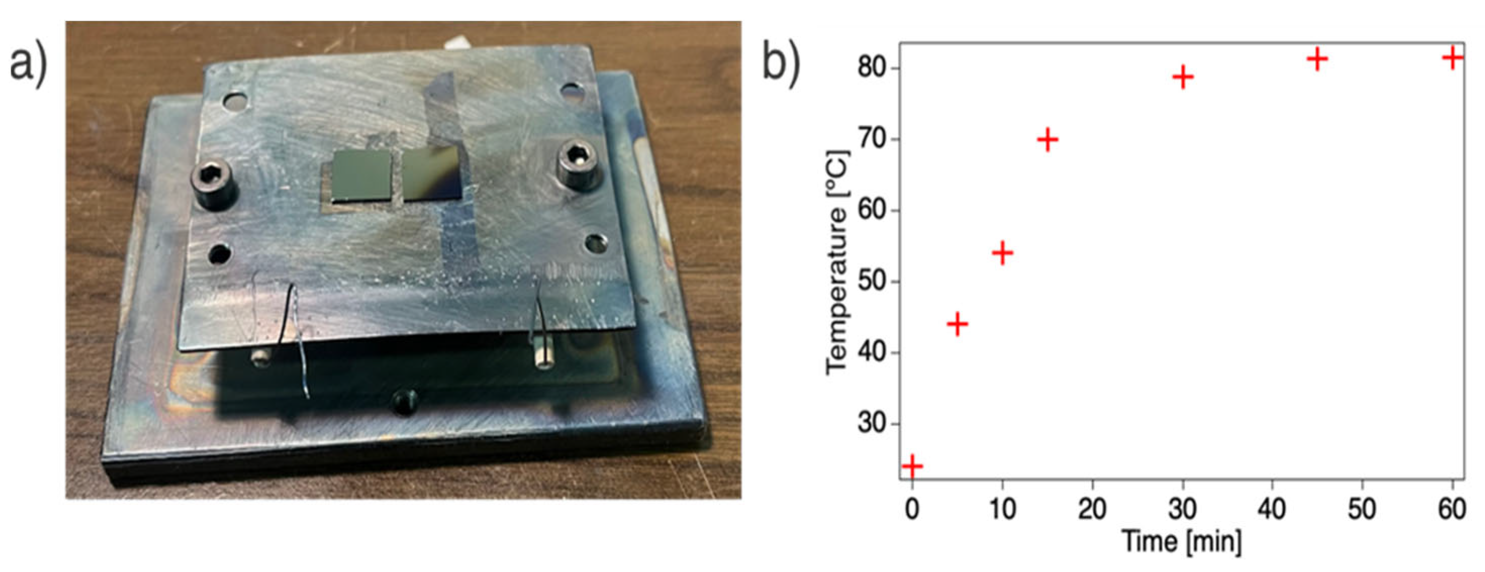
To evaluate the temperature behavior of the modified sample holder, the temperature was measured by placing a thermocouple directly on the thin plate while depositing at an acceleration voltage of 16 kV and a discharge frequency of 80 Hz. The resulting temperature profile, as shown in Figure 1b, indicates that within approximately 45 min, the thin plate reaches a constant temperature of ~80 °C. Hence, the modified sample holder enhances heat conduction and allows for faster heating promoted by the ablation plasma. Since the measurement shown in Figure 1b only reflects the plate’s surface temperature, it suggests that the local temperature in the plasma-impacted region of the sample holder is likely even higher, highlighting the thermal effects induced by plasma interaction.
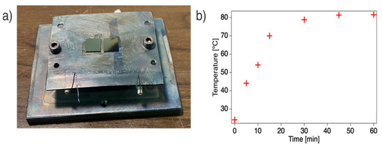
Figure 1.
(a) Photograph of the modified sample holder showing the thin plate mounted on top of the previous sample holder; (b) evolution of the temperature on the sample holder (thin plate) while depositing at 16 kV and 80 Hz.
Additionally, we adjusted the IJD source configuration by reducing the number of condensers from 12 to 6 and the number of resistors, consequently, thereby slightly decreasing the energy of each ablation and improving the discharge ignition phase. These modifications improve overall efficiency, reproducibility, and control over the IJD ablation process.
2.2. Thin Film Growth
The Pt substrates were prepared as thin films (thickness ~240 nm) on a Si wafer by electron beam evaporation [18] using a thin Cr adhesion layer, resulting in a Pt (240 nm)/Cr (5 nm)/Si structure. After sonicating the Pt substrates in isopropanol for 10 min, MoS2 thin films were deposited via IJD using an MoS2 cylindrical target acquired from Testbourne Ltd., Basingstoke, UK (Ø = 5 cm, thickness = 0.5 cm, purity 99.9%). The base pressure in the lab-grade IJD chamber was 5 × 10⁻⁶ mbar and increased to 1 × 10⁻³ mbar during plasma formation with Ar as the working gas. An acceleration voltage of 15 kV and a discharge frequency of 60 Hz were used. To investigate the bulk properties of MoS2 thin films, samples were deposited for a total period of 120 min, referred to as “as-deposited multilayer film”. To assess the influence of thermal self-heating of the sample holder during deposition, a three-step process was adopted. Following an initial continuous deposition for 60 min, the process was paused to allow partial cooling of the sample (without reaching room temperature) over 15–20 min. A second 60 min deposition cycle was then carried out, resulting in a total deposition time of 120 min.
To examine potential interactions between MoS2 and the Pt substrate, samples were deposited for 3 min, designated as “as-deposited interface film”. The as-deposited MoS2 samples were subsequently annealed in an ultra-high vacuum (UHV) environment (p = 2 × 10⁻⁹ mbar) at 270 °C for 300 min, resulting in annealed multilayer and interface films. The bare Pt substrate was used as reference material throughout the experiment.
2.3. Structural and Morphological Characterization
The XRD analysis was carried out using a powder diffractometer Rigaku D-MAX III (Rigaku Corporation, Tokyo, JPN) with a copper cathode and selecting the Cukα1 radiation (λ = 1.54056 Å). The measurements were taken in θ–2θ configuration in an interval from 10° to 70°, a step of 0.05° and an accumulation time of 2 s.
The Raman spectra were recorded using a Labram Aramis Jobin Yvon Horiba microRaman system (HORIBA Jobin Yvon, Stow, MA, USA) with a DPSS laser source of 532 nm and equipped with a confocal microscope and an air-cooled CCD. The pinhole was 100 μm. A 100× objective (0.8 NA) was used to focus the laser to collect the Raman signal. Spatial resolution was below 1 μm, and the power was around 5 mW. To acquire the spectra, an accumulation time of 5 s was used, and one scan per spot was taken.
AFM measurements were carried out using a HORIBA SmartSPM system (HORIBA France SAS, Palaiseau, France) in semi-contact mode, equipped with an HQ:NSC14/Al BS MikroMasch cantilever (force constant: 5 N/m, resonance frequency: 160 kHz). Scanning parameters included a 40 nm amplitude, 60% setpoint, and a 0.6 Hz scan rate. Data analysis was performed using Gwyddion v2.26 software [19], and the roughness was computed on the whole map averaging on single-row results.
Secondary electron (SE) images were acquired using a Helios 5 DualBeam focused ion beam–scanning electron microscope (FIB–SEM, Thermo Fisher, Waltham, MA, USA), operated at an acceleration voltage of 5 kV and a beam current of 50 pA. Imaging was performed in immersion mode using a through-the-lens detector (TLD).
Cross-sectional transmission electron microscopy (TEM) samples of the as-deposited and annealed MoS2 multilayer films were prepared with the FIB–SEM instrument. The TEM lamellae were transferred to dedicated copper TEM grids via a standard lift-out technique. The final polishing was performed using the Xe+ ions of the FIB source at 30 kV and 1.0–0.1 nA with an overtilt angle of 1°. TEM analysis was performed using a field-emission JEM-2200FS JEOL TEM (JEOL Ltd., Tokyo, Japan), equipped with an in-column Omega filter and operated at 200 kV.
2.4. Chemical Characterization
XPS and UPS measurements were conducted in a UHV analysis chamber, which is equipped with a non-monochromatized Mg Kα X-ray source (hν = 1254.6 eV) and a VSW HA100 hemispherical analyzer (with a PSP power supply and electronic control), providing a minimum energy resolution of 0.86 eV for XPS. The XPS binding energy (BE) scale was calibrated using the Au 4f peak at 84.0 eV as a reference. UPS characterization was performed using a He-discharge lamp with the He I emission line (21.22 eV) with an energy resolution of 0.1 eV and biasing the sample at −7 V.
3. Results
3.1. Multilayer Film
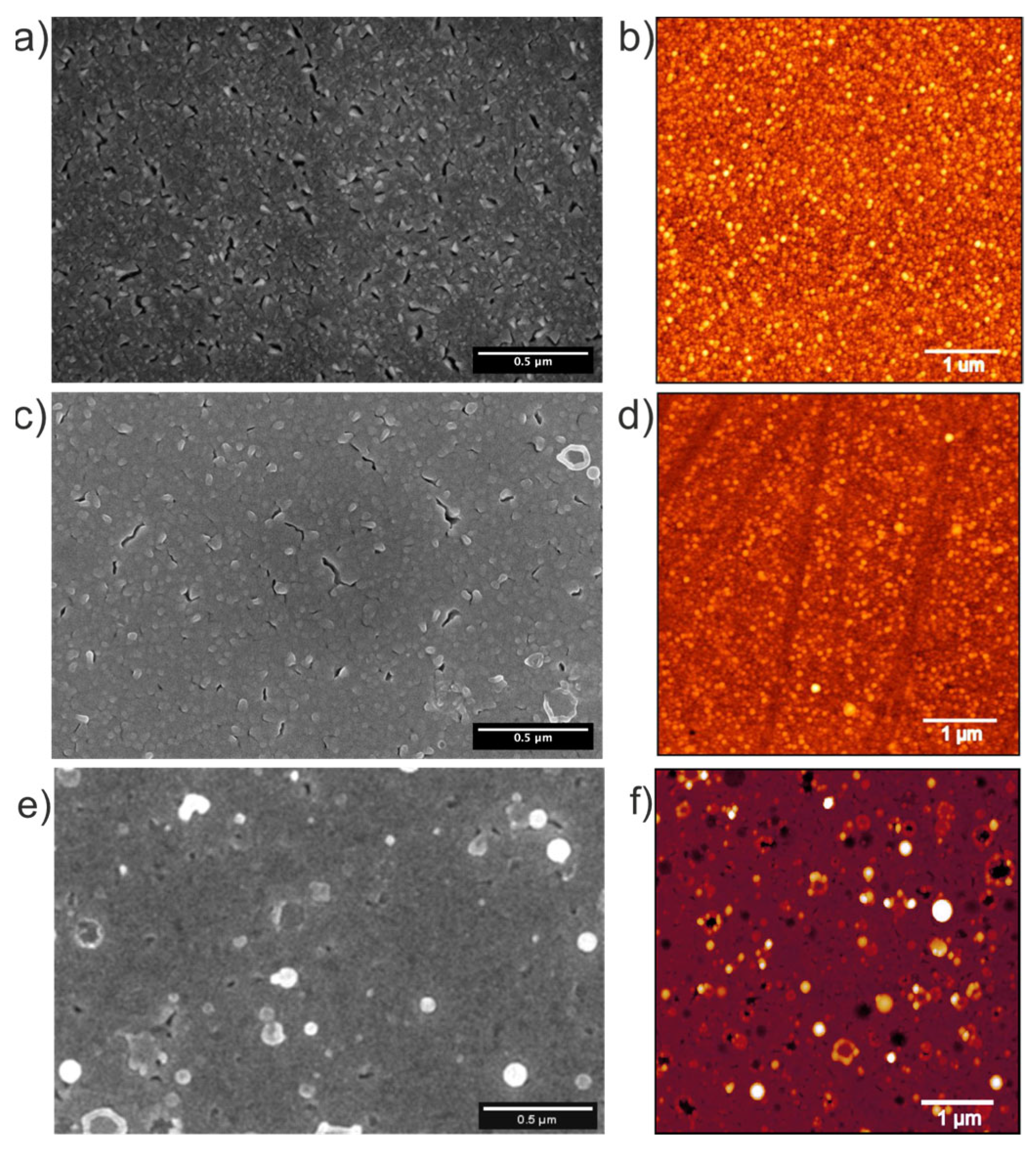
Figure 2 presents scanning electron microscopy (SEM) and atomic force microscopy (AFM) images of bare Pt substrate (Figure 2a,c) and as-deposited MoS2 interface film (Figure 2b,d), respectively.
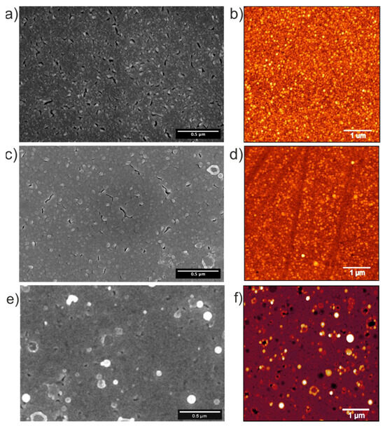
Figure 2.
SEM and AFM images of the (a,b) bare Pt substrate, the (c,d) as-deposited MoS2 interface, and the (e,f) multilayer film.
The bare Pt substrate in Figure 2a exhibits a rough surface morphology with uniformly distributed cracks with lengths in the order of 10s of µm. The AFM image in Figure 2b reveals that the Pt substrate has a surface roughness (root mean square, RMS) of ~5.5 nm. After 3 min of MoS2 deposition (as-deposited interface film in Figure 2c), it becomes obvious that the number of cracks and the overall roughness is slightly reduced due to the filling with MoS2. This agrees with the reduced RMS of ~4.7 nm, as measured from the AFM image in Figure 2d. After 120 min of deposition, the multilayer film exhibits the characteristic morphology previously reported in [15,17]—a smooth MoS2 thin film surface decorated with micron-sized, round-shaped particulates (droplets). These features are commonly observed in ablation-based deposition techniques and are attributed to the ejection of molten droplets or larger particulates from the target material [20].
The structural and strain characteristics of the as-deposited and annealed multilayer MoS2 film are shown in Figure 3. XRD analysis (Figure 3a) reveals a distinct peak at approximately 14°, indicative of the crystalline MoS2 already present in the as-deposited film. Upon annealing, the crystallinity of the MoS2 thin film improves slightly, as evidenced by the small increase in intensity and sharpness of the 14° peak.
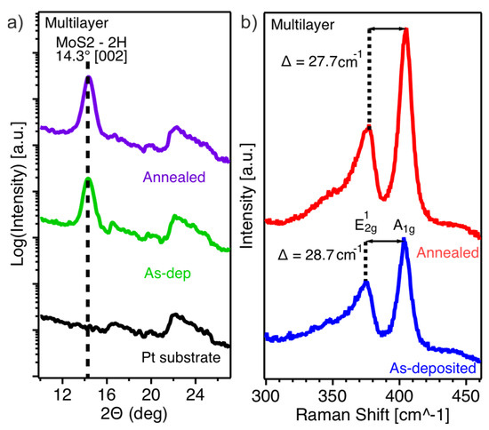
Figure 3.
(a) XRD spectra of the as-deposited and annealed MoS2 multilayer film; the spectrum of the bare Pt substrate is shown as a reference; (b) Raman spectra of the as-deposited and annealed multilayer film.
Raman spectroscopy of the as-deposited multilayer film (Figure 3b) shows the E12g (in-plane vibrational mode) and A1g (out-of-plane vibrational mode) components at 374.8 cm−1 and 403.5 cm−1, respectively. The Raman shift difference of 28.7 cm−1, which is higher than the expected value of 25 cm−1 for bulk MoS2, indicates the presence of strain in the as-deposited film. After annealing, the E12g mode shifts slightly towards higher wavenumbers, while the A1g mode remains nearly unchanged, resulting in a reduced Raman shift difference of 27.7 cm−1.
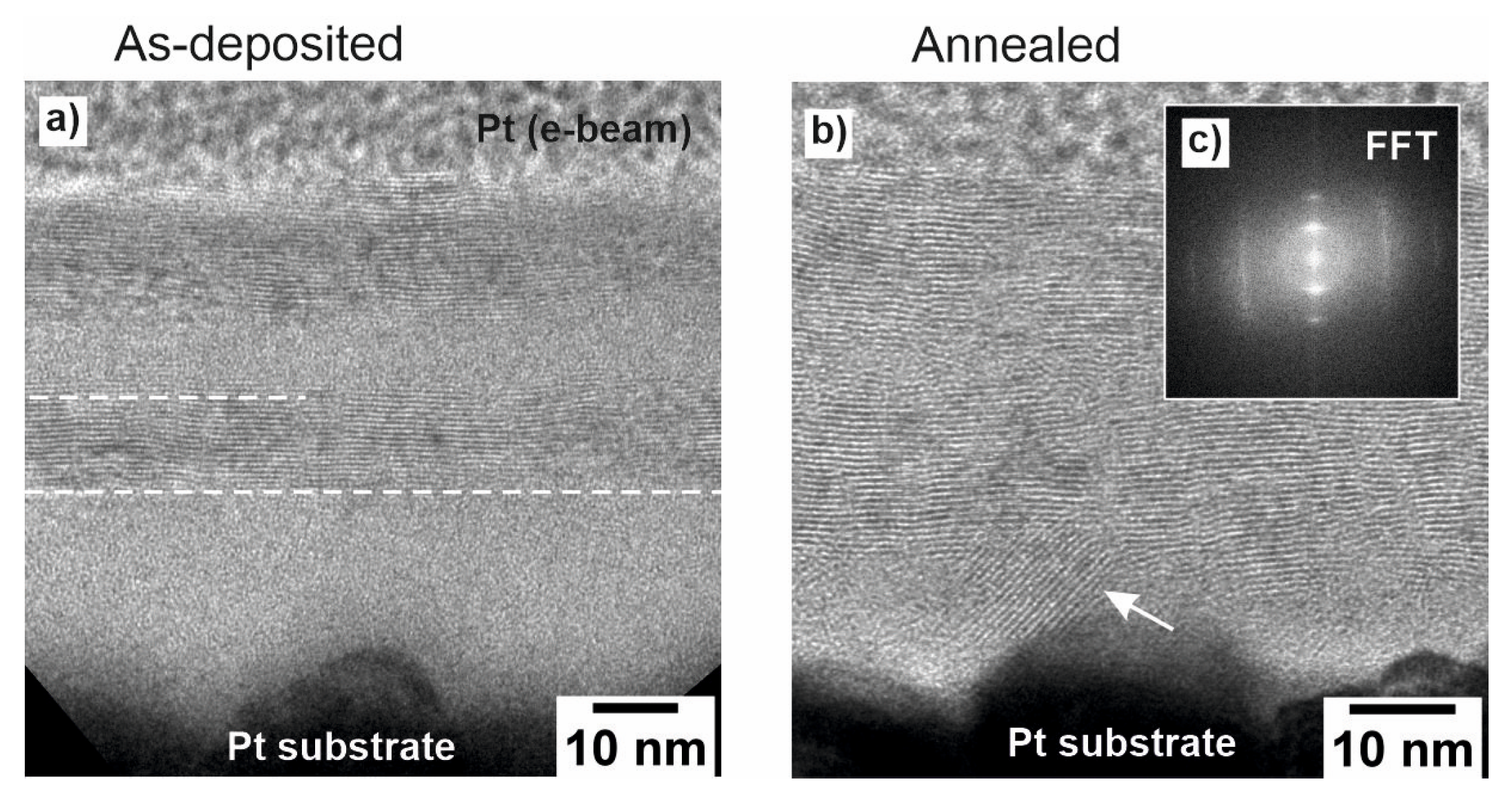
In the bright-field TEM image of the as-deposited multilayer film (Figure 4a), we observe a distinct sequence of structural transitions along the vertical growth direction. From the bottom to the top, the initial region appears amorphous, which can be attributed to the slow increase in substrate temperature during the early stages of IJD. As the temperature gradually increases and approaches saturation, a transition to crystalline growth is observed within the first 60 min of continuous deposition (indicated by the first dotted line in Figure 4a). This behavior aligns with the temperature profile measured on the sample holder during deposition (Figure 1b), suggesting that the initial temperature supports only the growth of amorphous MoS2, whereas the elevated temperature at later stages enables the formation of crystalline MoS2. After the cooling-down phase and during the second step of deposition, the substrate temperature increased once again, resulting in a renewed sequence of amorphous growth followed by crystalline growth, as the temperature reached its maximum value, which took less time due to the higher initial temperature of the substrate. This thermal evolution directly explains the alternating amorphous-to-crystalline morphology visible in the TEM image of the as-deposited multilayer film.
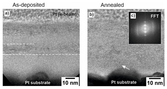
Figure 4.
(a,b) HRTEM images of the (a) as-deposited and (b) annealed multilayer film with the corresponding Fast Fourier Transform (FFT) pattern in the inset (c).
After thermal treatment at 270 °C in UHV, the annealed multilayer film (Figure 4b) exhibits crystalline MoS2 layers over the entire film, with reminiscent amorphous regions only close to the Pt substrate. It is assumed that the deposited material initially conforms to the roughness of the platinum substrate in an amorphous state before transitioning into layered growth when the sample holder reaches its maximum temperature due to plasma-induced heating (as shown in Figure 4a). Annealing at 270 °C further increases the crystallinity of the film. Figure 4c presents the Fast Fourier Transform (FFT) pattern obtained from the high-resolution TEM image of the annealed multilayer. The pattern exhibits hexagonal symmetry consistent with the zone axis of the 2H-MoS2 phase, thereby supporting the structural assignment made based on XRD analysis. Some layers close to the Pt substrate appear to be bent, most likely due to the substrate roughness (shown by the white arrow in Figure 4b). The overall thickness of the as-deposited/annealed multilayer film amounts to 45 nm.
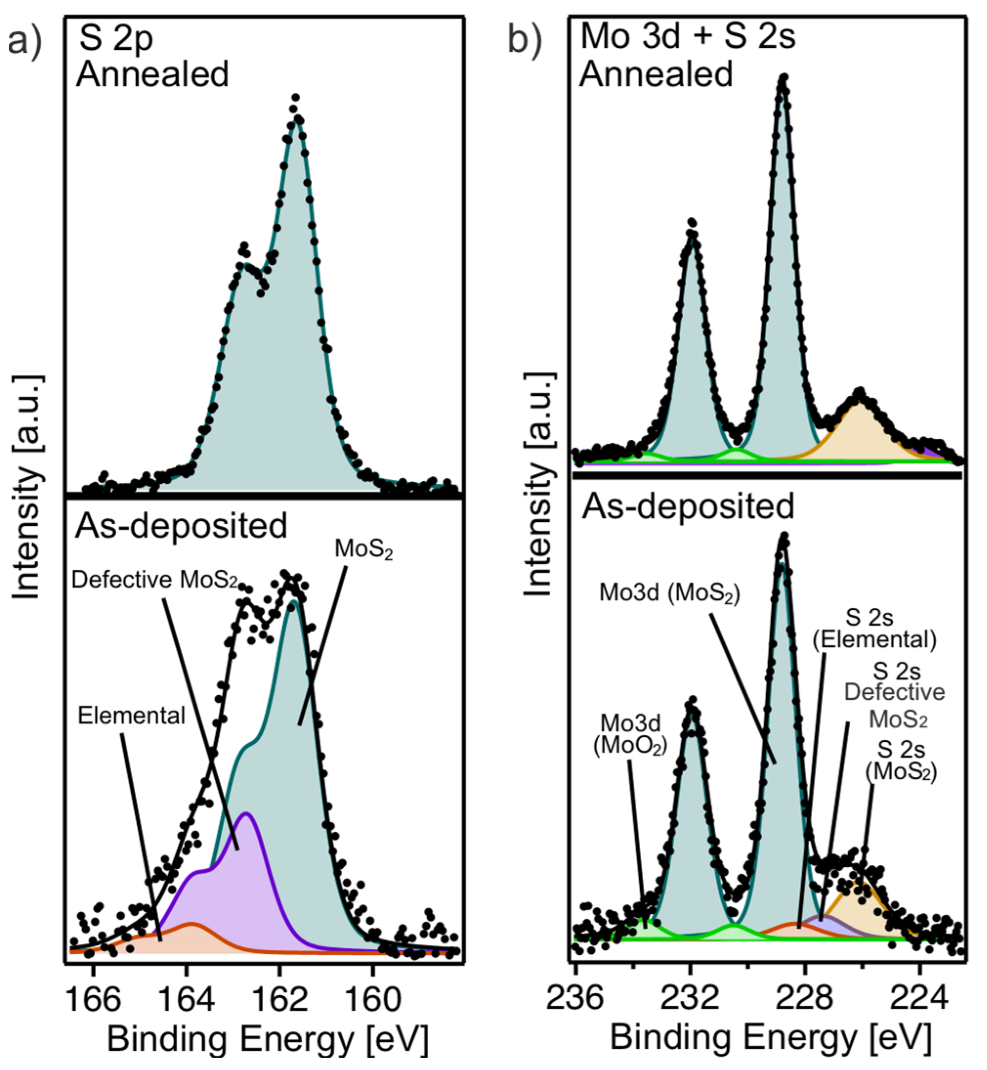
To understand the evolution of the chemical species in the multilayer film before and after annealing, we performed a comprehensive analysis of XPS core level components. The S 2p core level spectrum of the as-deposited multilayer film (Figure 5a, lower panel) displays significant broadening, attributable to multiple sulfur-related components. These include the S 2p component of highly defective MoS2 at 162.75 eV (violet), unbound elemental sulfur at 163.9 eV (red), and the characteristic S 2p signal of MoS2 at 161.65 eV (petrol). After annealing (Figure 5a, upper panel), the S 2p spectrum is only composed of a single component at 161.65 eV, corresponding to MoS2. This change indicates a loss of elemental sulfur after annealing and a significant reduction in sulfur-related defects, reflecting improved sample uniformity and crystallinity, as observed in our previous studies [15,17].
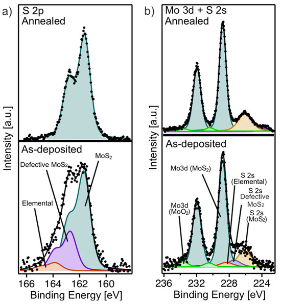
Figure 5.
(a) S 2p and (b) Mo 3d and S 2s core level spectra of as-deposited (lower panel) and annealed (upper panel) MoS2 multilayer film.
The Mo 3d core level of the as-deposited multilayer film (Figure 5b, lower panel) is observed at 228.85 eV, with an additional small peak at 230.50 eV corresponding to MoO2 (green). On the lower BE side, a broad shoulder corresponding to S 2s components was noted, consistent with features in the S 2p spectrum in Figure 5a (lower panel). After annealing, the intensity of the S 2s shoulder diminishes, in agreement with the reduction in sulfur-related features in the S 2p spectrum, while the binding energies of the Mo 3d components remain unchanged. In addition, the small component related to MoO2 further decreases. These results highlight the importance of the annealing process in improving the chemical purity and structural integrity of the MoS2 multilayer by eliminating sulfur-related defects and reducing oxidation states.
3.2. Interface Film
The XRD analysis of the as-deposited and annealed interface film (see Figure S1, Supporting Information) does not provide any valuable contribution because the deposited material is expected to be thinner than 5 nm. As a result, the XRD signal is dominated by the underlying Pt rather than the deposited layer itself. During the early stages of IJD growth, the deposited material fills the substrate’s roughness in an amorphous manner, preventing the formation of a well-defined crystalline structure even after annealing. This interpretation is consistent with the TEM observations in Figure 4, which clearly show the amorphous nature of the first deposited layers within the roughness of the Pt substrate and that this amorphous structure is maintained even after annealing.
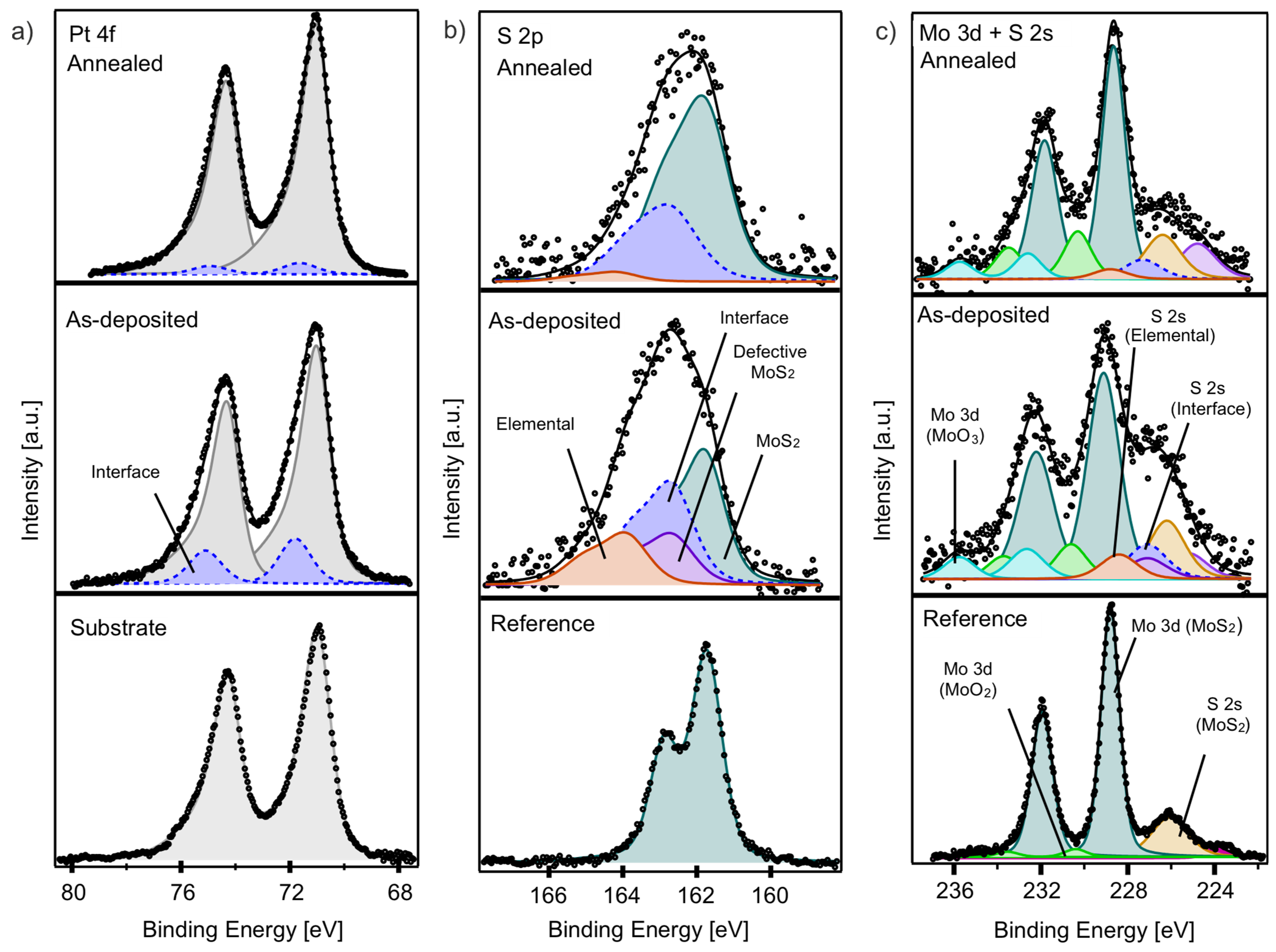
The XPS analysis of the interface film (Figure 6) reveals significant changes in the Pt 4f, S 2p, and Mo 3d core levels before and after annealing. The Pt 4f core level spectrum of the as-deposited interface film (Figure 6a, middle panel) shows slight broadening compared to the reference Pt 4f spectrum of the substrate (Figure 6a, lower panel), which features a Pt 4f 7/2 peak at 71.05 eV. This broadening necessitates the addition of a new component (dashed blue) at 71.80 eV, which significantly diminishes after annealing.
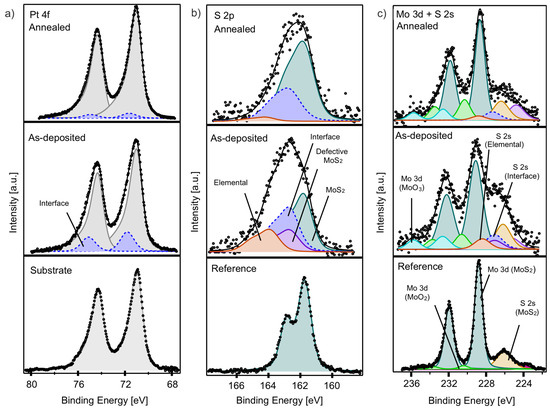
Figure 6.
(a) Pt 4f, (b) S 2p, and (c) Mo 3d and S 2s core level spectra of as-deposited (middle panels) and annealed interface film (upper panels); the lower panels show corresponding reference spectra of bare Pt substrate and bulk MoS2, respectively.
The S 2p core level spectrum of the as-deposited interface film (Figure 6b, middle panel) appears broad and is comprised of four distinct components: the S 2p of MoS2 at 161.76 eV, a component indicative of highly defective MoS2 at 162.75 eV, i.e., the same found in the multilayer film and with the same ratio (violet), a component at 162.75 eV (dashed blue) that we can attribute to Pt-S interface interaction, and elemental sulfur at 163.90 eV (red). After annealing, the component related to highly defective sulfur disappears, and the contributions from the elemental sulfur and the Pt-S interaction decrease, leading to a predominance of the MoS2 component. These changes suggest a transition towards a more uniform and crystalline MoS2 structure and reduced Pt-S interaction after annealing.
The Mo 3d core level spectrum of the as-deposited interface film (Figure 6c, middle panel) was found at 229.00 eV, accompanied by a MoO2 component (green) and a newly identified higher BE component at 232.60 eV, attributed to MoO3 (bright blue). A shoulder on the lower BE side corresponds to S 2s core levels associated with the sulfur components as previously identified in the S 2p spectrum (Figure 6b). After annealing, this shoulder becomes sharper, consistent with the disappearance of the highly defective sulfur and substantial desorption of elemental sulfur. The main Mo 3d peak shifts slightly to a lower BE (228.65 eV), indicating a reduction in Mo6+ species and an increased formation of Mo4+ species in MoS2, consistent with a decrease in the MoO3 component.
Figure 7 presents the UPS analysis of the bare Pt substrate, the as-deposited and annealed interface film, and the annealed multilayer film, illustrating the evolution of the electronic structure with increasing thickness and annealing. Figure 7a shows the secondary electron cut-off (SECO) spectra, from which the work function of each sample is determined. The bare Pt substrate has a work function of 4.38 eV, which slightly increases to 4.43 eV for the as-deposited interface film. Upon annealing, the work function further increases to 4.70 eV, reaching a maximum of 5.07 eV for the annealed multilayer film. This trend suggests that with increasing MoS2 thickness and crystallinity, the work function increases.
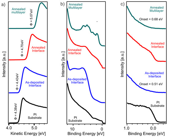
Figure 7.
(a) SECO and (b,c) valence band region UPS spectra of as-deposited and annealed interface film, annealed multilayer film, and Pt substrate, as indicated in the figure. (b) Extended region of the valence band spectra and (c) subsequent zoom into the near EF region.
Figure 7b displays the extended valence band region UPS spectra of the different films. The samples exhibit characteristic MoS2 valence band features in the BE range of 2 to 8 eV, which become increasingly pronounced with thickness. In the annealed multilayer film, these features are well-defined, confirming the presence of MoS2 states and their contribution to the electronic structure. The spectral shape is in agreement with previous reports on MoS2 [15,21], where the valence band originates from Mo 4d and S 3p hybridized states.
An enlarged view of the valence band near the Fermi level is shown in Figure 7c. The as-deposited interface film exhibits a valence band onset at 0.51 eV, whereas the annealed multilayer film shows a slightly higher onset at 0.68 eV. Notably, the annealed interface film exhibits the appearance of a Fermi edge, which is absent in the as-deposited state and in the multilayer film.
4. Discussion
The XPS analysis of the Mo 3d, S 2s, and S 2p core levels (Figure 5) provides strong evidence that the as-deposited MoS2 multilayer is already at least partially crystalline, differing from our previous studies of as-deposited MoS2 on SiO2/Si [17] and Pt substrates [15]. In previous works, the S 2p component associated with defective MoS2 was found to have an intensity comparable to that of stoichiometric MoS2. However, in the multilayer film of the present study, the crystalline component dominates, indicating that the material exhibits better structural order even in the as-deposited state. This suggests that the optimized IJD experimental setup with respect to that used for previous studies has yielded a MoS2 multilayer with fewer defects and a higher degree of long-range order.
The crystallinity of the material further improves upon annealing as evidenced by XRD measurements (Figure 3a). The characteristic peak at 14°, corresponding to the (002) plane of the 2H-MoS2 phase, further sharpens and slightly increases in intensity upon annealing.
Interestingly, the Raman spectra (Figure 3b) of the as-deposited multilayer film differ from those expected for bulk MoS2. The difference between the two main vibrational modes amounts to 28.7 cm−1, whereas in bulk MoS2, it is typically around 25 cm−1. The higher value suggests that the material experiences strain. Specifically, the in-plane vibrational component (E2g) is shifted toward lower wave numbers, indicating the presence of tensile strain. This strain is likely induced by the roughness of the substrate, which can cause local distortions and bending in the MoS2 layers. The TEM bright-field images of the as-deposited and annealed multilayer film (Figure 4a,b) support this interpretation. They show that the material initially conforms to the substrate roughness in an amorphous manner before transitioning to crystalline layered growth when the sample holder reaches its maximum temperature. Upon annealing, the difference between the two vibrational components in the Raman spectrum slightly reduces to 27.7 cm−1, suggesting a partial release of strain, likely due to atomic and layer rearrangements that reduce some of the substrate-induced distortions.
The TEM analysis in Figure 4a further reveals the growth mechanism and impact of annealing on the as-deposited MoS2. The material first fills the roughness of the substrate in an amorphous form, effectively adapting to the surface irregularities. Only after this initial amorphous filling, when the sample holder reaches its maximum temperature due to the ablation plasma, does the deposition transition into a mixture of layered and amorphous growth, where MoS2 adopts a more ordered structure. After annealing, the part of the film above the filled roughness becomes mostly crystalline. This observation aligns well with the XPS and XRD data, as it explains why the initial material has a significant crystalline contribution but still undergoes further structural improvement upon annealing.
In the interface film, the deposited MoS2 thickness is estimated to be less than 5 nm, i.e., the material initially fills the roughness of the substrate as an amorphous phase rather than forming distinct layered structures. As a result, the corresponding XRD analysis of both the as-deposited and annealed interface film (Figure S1, Supporting Information) does not show any crystalline contributions apart from those of the substrate. The lack of MoS2-related peaks in the XRD spectrum suggests that at this deposited thickness, the material remains in an amorphous state even after annealing, conforming to the substrate morphology without developing long-range order. This is consistent with the observations from the multilayer film, where, after annealing, transformation to crystalline layers only occurs after the initial “roughness-filling” growth phase.
XPS analysis of the Pt 4f and S 2p core levels of the interface film (Figure 6) provides further insight into the MoS2–Pt interface interactions. In the as-deposited interface film, additional components appear in these spectra, while the Mo 3d core level remains unchanged with respect to the as-deposited multilayer film. This indicates that the interaction at the Pt interface for the as-deposited film primarily involves the elemental sulfur, which is expected to form as clusters, rather than MoS2. Specifically, the Pt 4f spectrum shows a higher BE component, while the S 2p spectrum displays an additional component between the typical signal for elemental sulfur and the MoS2-related component. The fact that no shift is observed in the Mo 3d core levels suggests that MoS2 itself does not significantly interact with the Pt substrate. Instead, the interaction likely involves isolated sulfur clusters at the interface, which modify the electronic environment of Pt without affecting the MoS2 lattice. Even though the new experimental setup allows for a transition to crystalline growth already in the as-deposited film, annealing further improves the crystallinity of the as-deposited material, as observed in the annealed multilayer film. However, another key effect of the post-annealing step is the desorption of elemental sulfur. This is evidenced by the disappearance of the additional component in the S 2p core level related to sulfur clusters and the reduction in interface-related features in the Pt 4f spectrum. The loss of these sulfur clusters suggests that post-annealing promotes sulfur desorption, thereby reducing interface interactions and potentially leading to a cleaner MoS2–Pt interface. Further confirmation of sulfur desorption comes from UPS analysis (Figure 7). In the as-deposited interface film, the UPS spectra show a valence band onset at 0.51 eV, indicating a fully covered platinum substrate. After annealing, the UPS spectra reveal the emergence of a Fermi edge, which is most likely associated with the desorption of elemental sulfur. This desorption reduces the interaction at the interface and likely exposes portions of the platinum substrate.
5. Conclusions
This study investigated the growth and properties of MoS2 thin films deposited onto technologically relevant platinum substrates via IJD. The results show that modifications to the IJD system enhanced heat conduction and plasma-induced heating, allowing crystalline MoS2 growth without requiring high-temperature annealing. Further crystallinity improvements to produce high-quality MoS2 thin films are reached after post-deposition annealing. Structural characterization using XRD, Raman spectroscopy, and TEM confirmed an amorphous-to-crystalline transition, further improved by annealing. The platinum substrate’s roughness influences the strain in the MoS2 layers, while annealing reduces sulfur-related defects, enhancing film integrity, as shown by XPS analysis. The MoS2–Pt interface reveals Pt-S bonds that decrease upon annealing. UPS analysis demonstrated that the electronic properties of MoS2 films improve with thickness and annealing, showing an increase in work function and the development of MoS2-specific valence band features. In conclusion, this work provides insights into optimizing MoS2 growth on platinum using IJD, highlighting how process parameters influence the structural, chemical, and electronic properties of the films. These findings contribute to the development of MoS2 for applications in catalysis, electronics, and energy storage.
Supplementary Materials
The following supporting information can be downloaded at: https://www.mdpi.com/article/10.3390/surfaces8020038/s1, Figure S1: XRD on interface film; Table S1: Fitted XPS parameters.
Author Contributions
C.T.C.: methodology, formal analysis, investigation, data curation, visualization, and writing—original draft. C.G.: partial data acquisition and writing—review and editing. A.P.: partial data acquisition and interpretation and writing—review and editing. L.N.: writing–review and editing, data acquisition, and data interpretation. F.R.: writing—review and editing, data acquisition, and data interpretation. A.C.: writing—review and editing and data acquisition. R.C.: data acquisition and partial interpretation. R.V.: writing—review and editing, data interpretation, and supervision, M.V.N.: data interpretation, data curation, supervision, and resources. M.T.: writing—review and editing, supervision, resources, project administration, funding acquisition, and conceptualization. All authors have read and agreed to the published version of the manuscript.
Funding
This research was funded by the Italian MUR under PRIN 2022 Project ‘2D-EMMA’ (Project n. 202289PMBP, CUP: B53D23004010006), under PRIN 2022 Project ‘PETRA’ (Project n. 2022T7ZSEK, CUP B53D23001860006) and under PNRR 2023 Project ‘NQSTI’ (Project n. PE0000023, CUP B53C22004180005) in the frame of Next Generation EU.
Institutional Review Board Statement
Not applicable.
Informed Consent Statement
Not applicable.
Data Availability Statement
Data is contained within the article or Supplementary Materials.
Acknowledgments
The authors would like to thank L. Lorenzelli for providing the Pt substrates.
Conflicts of Interest
The authors declare no conflicts of interest.
References
- Bernardi, M.; Ataca, C.; Palummo, M.; Grossman, J.C. Optical and Electronic Properties of Two-Dimensional Layered Materials. Nanophotonics 2015, 6, 479–493. [Google Scholar] [CrossRef]
- Ye, M.; Winslow, D.; Zhang, D.; Pandey, R.; Yap, Y.K. Recent advancement on the optical properties of two-dimensional molybdenum disulfide (MoS2) thin films. Photonics 2015, 2, 288–307. [Google Scholar] [CrossRef]
- Kowalczyk, D.A.; Rogala, M.; Szałowski, K.; Kozłowski, W.; Lutsyk, I.; Piskorski, M.; Krukowski, P.; Dąbrowski, P.; Belić, D.; Cichomski, M.; et al. Local electronic structure of stable monolayers of α-MoO3−x grown on graphite substrate. 2D Mater. 2020, 8, 025005. [Google Scholar] [CrossRef]
- Samadi, M.; Sarikhani, N.; Zirak, M.; Zhang, H.; Zhang, H.L.; Moshfegh, A.Z. Group 6 transition metal dichalcogenide nanomaterials: Synthesis, applications and future perspectives. Nanoscale Horiz. 2018, 3, 90–204. [Google Scholar] [CrossRef] [PubMed]
- Xi, X.; Wang, Z.; Zhao, W.; Park, J.H.; Law, K.T.; Berger, H.; Forró, L.; Shan, J.; Mak, K.F. Ising pairing in superconducting NbSe2 atomic layers. Nat. Phys. 2016, 12, 139–143. [Google Scholar] [CrossRef]
- Bussolotti, F.; Chai, J.; Yang, M.; Kawai, H.; Zhang, Z.; Wang, S.; Wong, S.L.; Manzano, C.; Huang, Y.; Chi, D.; et al. Electronic properties of atomically thin MoS2 layers grown by physical vapour deposition: Band structure and energy level alignment at layer/substrate interfaces. RSC Adv. 2018, 8, 7744–7752. [Google Scholar] [CrossRef] [PubMed]
- Karmakar, S.; Biswas, S.; Kumbhakar, P. A comparison of temperature dependent photoluminescence and photo-catalytic properties of different MoS2 nanostructures. Appl. Surf. Sci. 2018, 455, 379–391. [Google Scholar] [CrossRef]
- Palencia-Ruiz, S.; Uzio, D.; Legens, C.; Laurenti, D.; Afanasiev, P. Stability and catalytic properties of 1T-MoS2 obtained via solvothermal synthesis. Appl. Catal. A Gen. 2021, 626, 118355. [Google Scholar] [CrossRef]
- Jiao, Y.; Hafez, A.M.; Cao, D.; Mukhopadhyay, A.; Ma, Y.; Zhu, H. Metallic MoS2 for High Performance Energy Storage and Energy Conversion. Small 2018, 14, 1800640. [Google Scholar] [CrossRef] [PubMed]
- Mahlouji, R.; Verheijen, M.A.; Zhang, Y.; Hofmann, J.P.; Kessels, W.M.; Bol, A.A. Thickness and Morphology Dependent Electrical Properties of ALD-Synthesized MoS2 FETs. Adv. Electron. Mater. 2022, 8, 2100781. [Google Scholar] [CrossRef]
- Surucu, O.; Isik, M.; Gasanly, N.M.; Terlemezoglu, M.; Parlak, M. Temperature-tuned band gap properties of MoS2 thin films. Mater. Lett. 2020, 275, 128080. [Google Scholar] [CrossRef]
- Liao, L.; Kovalska, E.; Regner, J.; Song, Q.; Sofer, Z. Two-Dimensional Van Der Waals Thin Film and Device. Small 2024, 20, 2303638. [Google Scholar] [CrossRef] [PubMed]
- Lotti, R.; Elettra-Sincrotrone Trieste S.C.p.A. Apparatus and Method for Depositing Thin Films by Ionized Jet Deposition. U.S. Patent 8,803,425 B2, 12 August 2014. [Google Scholar]
- Skočdopole, J.; Lojka, M.; Hlásek, T.; Antončík, F.; Jankovský, O.; Kalvoda, L. Influence of Substrate Temperature on the Morphology and Phase Composition of Thin Films Prepared From Y-123 Targets by the IJD Method. IEEE Trans. Appl. Supercond. 2023, 33, 7500604. [Google Scholar] [CrossRef]
- Timpel, M.; Ligorio, G.; Ghiami, A.; Gavioli, L.; Cavaliere, E.; Chiappini, A.; Rossi, F.; Pasquali, L.; Gärisch, F.; List-Kratochvil, E.J.; et al. 2D-MoS2 goes 3D: Transferring optoelectronic properties of 2D MoS2 to a large-area thin film. NPJ 2D Mater. Appl. 2021, 5, 64. [Google Scholar] [CrossRef]
- Campedelli, E.; Mazzucato, M.; Parnigotto, M.; Pedrielli, A.; Gatsios, C.; Badocco, D.; Pastore, P.; Timpel, M.; Nardi, M.V.; Durante, C. Ionized Jet Deposition of MoS2 on Gas Diffusion Layer Electrodes for Next Generation Alkaline Electrolyzers. Adv. Sustain. Syst. 2025, 9, 2400979. [Google Scholar] [CrossRef]
- Ghiami, A.; Timpel, M.; Chiappini, A.; Nardi, M.V.; Verucchi, R. Synthesis of MoS2 Thin Film by Ionized Jet Deposition: Role of Substrate and Working Parameters. Surfaces 2020, 3, 683–693. [Google Scholar] [CrossRef]
- Prusakova, V.; Armellini, C.; Carpentiero, A.; Chiappini, A.; Collini, C.; Dirè, S.; Ferrari, M.; Lorenzelli, L.; Nardello, M.; Normani, S.; et al. Morphologic, structural, and optical characterization of sol-gel derived TiO2 thin films for memristive devices. Phys. Status Solidi (c) 2015, 12, 192–196. [Google Scholar] [CrossRef]
- Nečas, D.; Klapetek, P. Gwyddion: An open-source software for SPM data analysis. Open Phys. 2012, 10, 181–188. [Google Scholar] [CrossRef]
- Garrido, J.M.C.; Silveyra, J.M. A review of typical PLD arrangements: Challenges, awareness, and solutions. Opt. Lasers Eng. 2023, 168, 107677. [Google Scholar] [CrossRef]
- Kim, T.; Kang, D.; Lee, Y.; Hong, S.; Shin, H.G.; Bae, H.; Yi, Y.; Kim, K.; Im, S. 2D TMD Channel Transistors with ZnO Nanowire Gate for Extended Nonvolatile Memory Applications. Adv. Funct. Mater. 2020, 30, 2004140. [Google Scholar] [CrossRef]


Disclaimer/Publisher’s Note: The statements, opinions and data contained in all publications are solely those of the individual author(s) and contributor(s) and not of MDPI and/or the editor(s). MDPI and/or the editor(s) disclaim responsibility for any injury to people or property resulting from any ideas, methods, instructions or products referred to in the content. |
© 2025 by the authors. Licensee MDPI, Basel, Switzerland. This article is an open access article distributed under the terms and conditions of the Creative Commons Attribution (CC BY) license (https://creativecommons.org/licenses/by/4.0/).