Abstract
Porous PZT films offer significant potential due to tunable electromechanical properties, yet the polarization behavior remains insufficiently understood because of discontinuous morphology and domain structures. In this work, we study the impact of porosity on the spontaneous polarization and electromechanical response of PZT thin films fabricated using a multilayer spin-coating technique with various concentrations (0–14%) of polyvinylpyrrolidone (PVP) as a porogen. Atomic force microscopy (AFM) and piezoresponse force microscopy (PFM) were employed to analyze the local topography, domain distribution, and polarization behavior of the films. The results indicate that increasing porosity leads to substantial changes in grain morphology, dielectric permittivity, and polarization response. Films with higher porosity exhibit a more fragmented polarization distribution and reduced piezoresponse, while certain orientations demonstrate enhanced domain mobility. Despite the decrease in overall polarization, the local coercive field remains relatively stable, suggesting structural stability during the local polarization switching. The findings highlight the crucial role of grain boundaries and local charge redistribution in determining local polarization behavior.
1. Introduction
Dense PZT structures offer higher mechanical strength and thermal stability, making them ideal for applications requiring durability and reliability, such as composite heterostructures [1], energy-harvesting devices [2], sensor technologies [3], ultrasonic devices [4], Micro-Electro-Mechanical Systems (MEMS) [5], flexible electronics, and actuators [6,7]. While BaTiO3 was historically used in piezoelectric devices [8], PZT has become the preferred material due to its superior piezoelectric properties and higher Curie temperature, ensuring better performance in various technological applications. While the materials discussed above are typically utilized in their dense polycrystalline form, there are studies that highlight the potential applications of porous ferroelectric materials in energy technologies [9]. Porous piezoelectric ceramics [10,11], designed with controlled porosity, offer several advantages over traditional dense ceramics, including enhanced piezoelectric performance, improved mechanical flexibility, and tailored dielectric properties [12].
Local microstructural features of porous PZT piezoceramics significantly impact their mechanical performance for practical applications, but by employing a multiscale regulation strategy, a well-balanced mechanical performance in PZT piezoceramics has been successfully achieved [13]. In particular, the gradient porous structure of PZT ceramics has been demonstrated to significantly improve both mechanical and piezoelectric properties, which are essential for energy-harvesting applications [14,15]. The strategic alignment of porosity within PZT ceramics was found to enhance the pyroelectric and piezoelectric properties, thereby increasing their efficiency in various technological applications [16].
Of particular interest is PZT in the form of porous films, whose properties can be controlled by changing the porous structure. To optimize these properties, the introduction of an organic polymer (or porogen) is proposed as a viable approach (template method). During annealing, the porogen undergoes decomposition, leading to the formation of a porous structure. Various porogens such as polyethyleneimine [17], polyvinyl acetamide [18], polyethylene glycol [19], and polyvinyl pyrrolidone (PVP) [20,21] can be used in the template method. The resulting pores in these materials can be either open or closed. By adjusting the porogen concentration, the pore size can be controlled, which in turn affects the final properties of the functional material [22]. Currently investigating the influence of structural porosity on the piezoelectric properties of films, as well as examining the relationship between the porogen parameters and the resulting pore characteristics in the films is an urgent and crucial task in this direction of studies. Understanding these dependencies will enable the prediction of film quality prior to the fabrication. Compared to traditional dense films, porous films offer several advantages. Firstly, increased porosity enhances the surface area and film thickness [23,24]. However, depending on the geometry and number of pores, the ferroelectric properties of the material may also be altered [24,25,26,27]. The formation of porous PZT sol–gel films with high electrical parameters is complicated by the properties of the corresponding film-forming solutions.
In PZT film-forming solutions, zirconium and titanium alkoxides are traditionally used. Lead acetate trihydrate is used as the lead component, which is sensitive to moisture and requires dehydration for dissolution. Because of this, the range of porogens for forming homogeneous films is limited. PVP acts as a structure-directing agent that decomposes during heat treatment, creating well-defined and uniformly distributed pores within the PZT film. The pore size and morphology can be finely tuned by adjusting the molecular weight and concentration of PVP, allowing control over pore size [20,28]. Adding PVP increases the viscosity of the precursor solution, which can lead to thicker films after deposition. PVP also suppresses premature condensation reactions in the sol–gel process through hydrogen bonding, promoting structural relaxation and better film uniformity [18,29]. PVP’s thermal decomposition behavior is well understood, with complete removal occurring around 550 °C, which facilitates reproducible pore formation without leaving residues that degrade film quality [20].
In summary, PVP is advantageous as a porogen in PZT film fabrication because it enables precise control over pore structure and film thickness, improves microstructural quality, and allows tuning of electrical properties, all while maintaining stable and reproducible processing conditions.
In this work, by using atomic force microscopy (AFM) and piezoresponse force microscopy (PFM) methods, we investigate the performance of PZT thin films via studying the surface morphology and local piezoelectric properties in the presence of porogen polyvinylpyrrolidone (PVP).
2. Materials and Methods
The Pb(Zr0.48 Ti0.52) O3 (PZT) films were deposited on Si-SiO2-TiO2-Pt substrates using a multilayer deposition method from precursor solutions with a 15% Pb excess and the addition of 0–14% polyvinylpyrrolidone (PVP) with a molecular weight of 360,000. The initial data for the studied series are presented in Table 1.

Table 1.
Samples parameters.
The PVP-assisted sol–gel process was used for the preparation of the film-forming solution. For the preparation of PZT film-forming solutions, dry lead acetate was used, synthesized from PbO following the methodology described in [30]. Zirconium isopropoxide (99.9%, Aldrich, Saint Louis, MO, USA) and titanium isopropoxide (99.999%, Aldrich) were used without additional purification. The Zr/Ti ratio was maintained at 48/52. To compensate for PbO loss during annealing, an excess of 14 mol.% Pb was added to the film-forming solution relative to the stoichiometric composition.
The PZT films were deposited layer by layer to achieve the required thickness using a spin-coating method on platinum-coated substrates with the following structure: Si-SiO2 (300 nm)-TiO2 (10 nm)-Pt (150 nm) (Inostek, Seoul, Korea). Each deposited layer was dried using an IR lamp at approximately 200 °C for 5 min (soft drying) and annealed at 400 °C for 10 min to remove organic residues. After applying the final layer, the PZT films were crystallized at 650 °C for 15 min. The film thickness (d) and refractive index (n) were measured using spectral ellipsometry (SE850 from Sentech Instruments GmbH, Berlin, Germany). The relative porosity was estimated using the Lorentz–Lorenz equation.
The PVP360000 concentration shows a strong correlation with several other parameters in Table 1. As the PVP concentration increases from 0% to 14%, we observe a decreasing number of layers. The number of deposited layers decreases from 10 (at 0% PVP) to 3 (at 14% PVP). This suggests that higher polymer content enables thicker individual layers, requiring fewer deposition steps to achieve similar overall thickness. The relative porosity increases dramatically from 0% (no PVP) to 33.3% (6.6% PVP), demonstrating that PVP acts as a pore-forming agent or template in these films. The polymer likely creates void spaces within the film structure during deposition or subsequent processing. The refractive index decreases significantly from 2.543 (0% PVP) to 1.829 (6.6% PVP), showing an inverse relationship with porosity. This aligns with effective medium theory predictions, where increased air-filled pores lower the effective refractive index of the composite material.
The effect of polymer porogen concentration on PZT film topography was analyzed using commercial atomic force microscope (Ntegra Prima, NT-MDT, Moscow, Russia) equipped with NSC15/Pt (resonance frequency 325 kHz, spring constant 40 N/m, MikroMasch, Sofia, Bulgaria) and also employed in piezoresponse force microscopy (PFM) mode for the study of local piezoelectric properties [31]. For this, an external voltage in the range of ±10 V was applied to the cantilever, while the sample structure remained grounded.
Topographical analysis of the samples studied was conducted using scanning electron microscopy (SEM, Jeol, Tokyo, Japan). A commercial scanning electron microscope Nova NanoSEM was employed to obtain the images. Microstructural investigations were performed under the following parameters: magnification of 100,000×, accelerating voltage of 10 kV, and working distance of 5.3 mm.
3. Results and Discussion
3.1. Analysis with an X-Ray Diffractometer
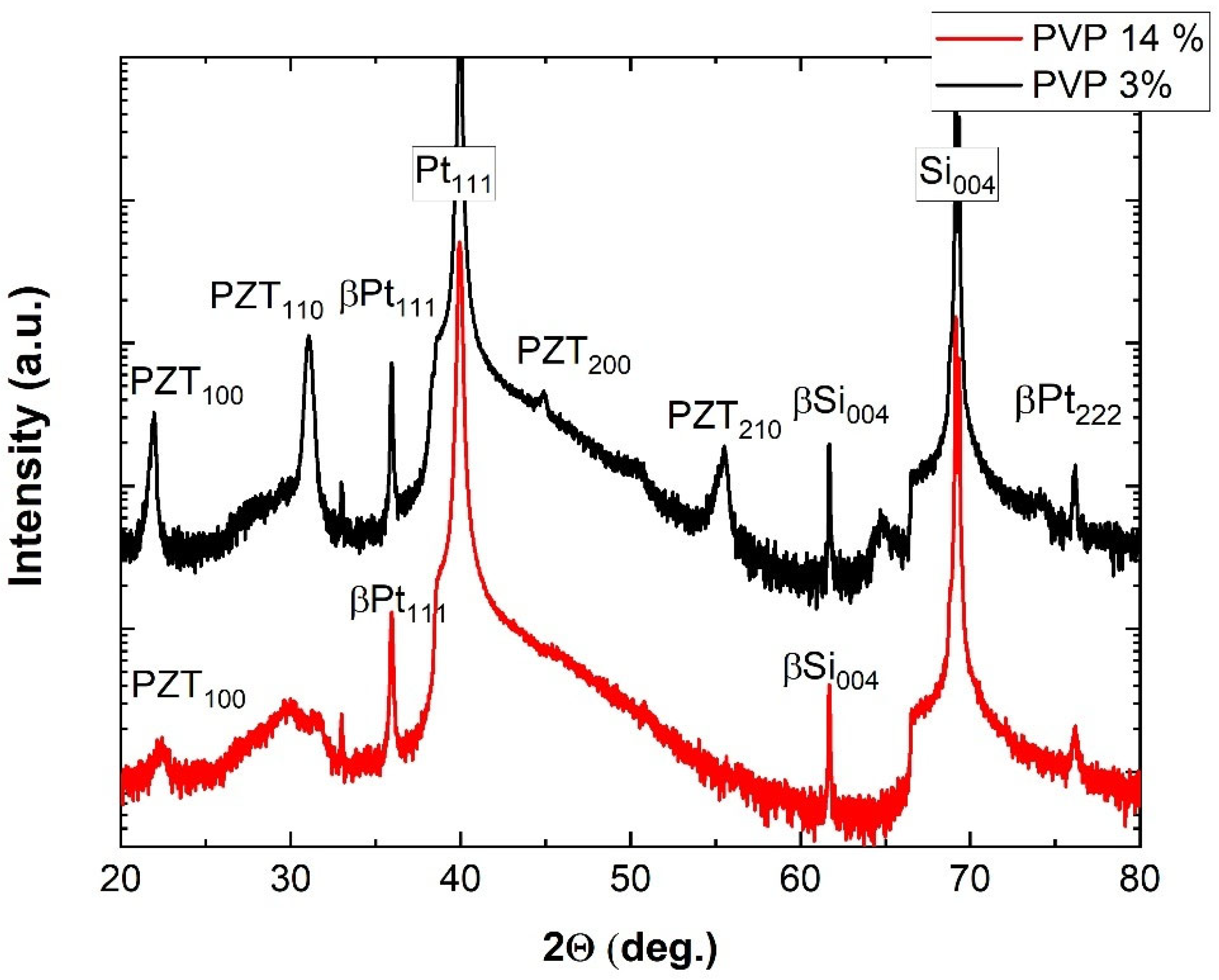
To confirm the crystallinity of the PZT films, diffractograms were obtained for samples with 3% and 14% PVP content (Figure 1). The diffractograms of the rest of the series were presented in [32]. A DRON-8T diffractometer in a non-monochromator configuration at 40 kV and 20 mA current on an X-ray tube was used to obtain the diffractograms. The tube has a Soller slit and a 0.5 mm wide equatorial slit. A Soller slit, a 0.25 mm wide equatorial slit, and a nickel beta filter were used on the detector. The scanning was carried out using a discrete method with a step of 0.02 degrees; the signal accumulation time for one point was 15 s.
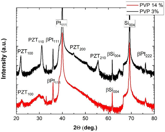
Figure 1.
Diffractogram of the sample with 3% PVP addition (red line) and the sample with 14% PVP addition (black line).
The diffractogram of the sample with 3% PVP addition (Figure 1, red line) shows peaks corresponding to the PZT phase located at angles 22°, 31°, 45°, 55.5°, which are identified with orientations (100), (110), (200), (210). The sample is polycrystalline. In addition, the diffractogram shows peaks related to the phases of Pt, Si. The diffractogram of the sample with 14% PVP addition (Figure 1, black line) also demonstrates Pt and Si peaks. However, the peaks corresponding to PZT have almost completely disappeared, with only weakly pronounced (100) and (110) crystallographic reflections remaining. The obtained results demonstrate good agreement with previous findings reported in [33], where X-ray diffraction analysis was employed to investigate residual stresses in PZT thin films fabricated via pulsed laser deposition. This consistency provides strong evidence that the studied samples maintain a perovskite phase structure.
3.2. Analysis of Local Surface Morphology Using SEM
The utilized configuration of SEM allowed for the obtaining of detailed high-resolution images of the surface morphology of the samples (Figure 2).
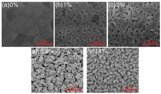
Figure 2.
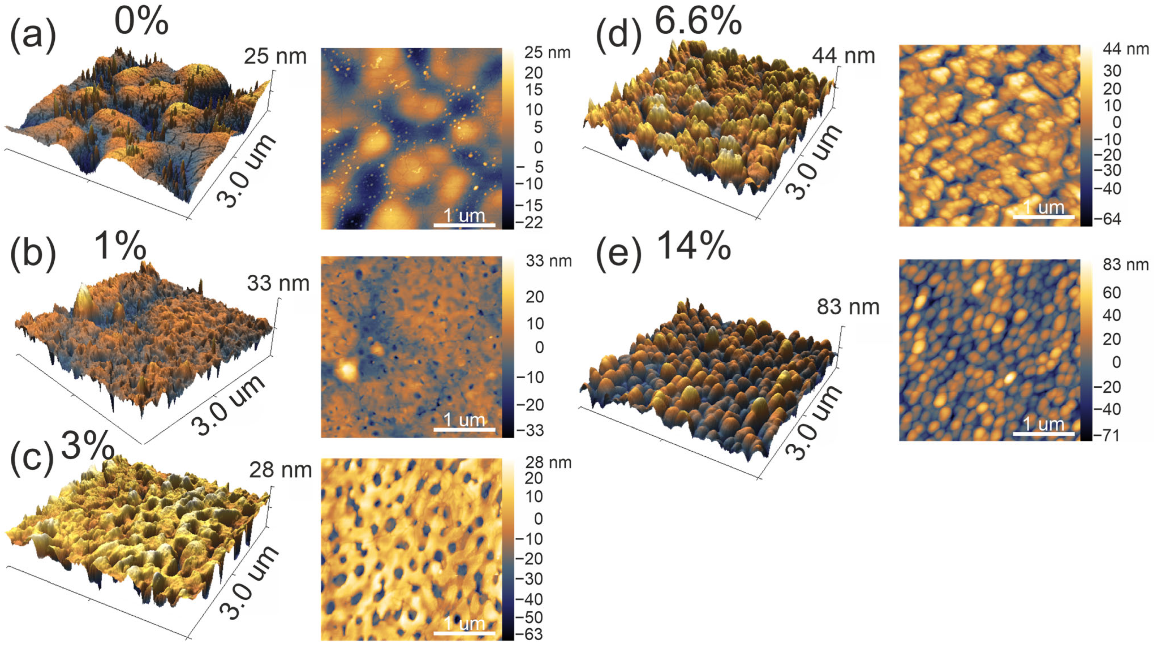
Surface images obtained by SEM for the sample with 0% PVP content (a), for the sample with 1% PVP content (b), for the sample with 3% PVP content (c), for the sample with 6.6% PVP content (d), for the sample with 14% PVP content (e).
The sample with 0% PVP content (Figure 2a) displays a relatively smooth, continuous surface with minimal texture and few distinguishable features. The surface appears largely homogeneous with some subtle grain boundaries or minor irregularities visible across the field of view. In contrast, the introduction of just 1% PVP (Figure 2b) induces a dramatic structural change, with the emergence of numerous small pores distributed across the surface. These pores appear relatively uniform in size and demonstrate consistent spacing throughout the material. At 3% PVP content (Figure 2c), the evolution of surface morphology continues with a notable increase in both pore size and density. The pores appear larger, more defined, and potentially deeper compared to those observed in the 1% PVP sample. The spaces between pores have become thinner, suggesting a progressive transformation toward a more interconnected porous network.
A fundamental shift in morphology occurs at 6.6% PVP content (Figure 2d), where the structure no longer resembles a continuous matrix with pores but instead appears as an assembly of discrete particles. These particles create a highly porous, interconnected network with significant void space between the individual elements. The particles appear somewhat irregular in size and arrangement, creating a complex three-dimensional structure. The sample with the highest PVP content of 14% (Figure 2e) maintains the particulate nature observed at 6.6% but exhibits notable refinement. The particles appear more uniform in size, more spherical, and demonstrate a more ordered arrangement with denser packing.
The progression from 0% to 14% PVP content reveals several key trends in material structure. First, there is a clear increase in overall porosity and surface area with increasing PVP concentration. The initial formation of isolated pores eventually gives way to a highly porous network and finally to a particulate structure with interstitial spaces. The transition from a porous continuous matrix to a particulate structure represents a fundamental change in material architecture. This suggests that PVP may be functioning not only as a porogen (pore-forming agent) at lower concentrations but potentially as a structure-directing agent or particle growth modifier at higher concentrations. Additionally, the increasing uniformity and ordered arrangement of particles at the highest PVP concentration indicate that PVP may influence nucleation and growth mechanisms, potentially by controlling aggregation processes or surface energetics.
3.3. Analysis of Local Surface Morphology Using AFM
The analysis of PZT film topography with varying polyvinylpyrrolidone (PVP) concentrations revealed significant structural transformations depending on the porogen content (Figure 3).

Figure 3.
Topography of the studied sample series with PVP content of 0% (a), 1% (b), 3% (c), 6.6% (d), and 14% (e).
The 0% PVP sample exhibited a granular surface morphology with a maximum grain height of 18 nm and an average grain boundary width of 15 nm. Porogen particles, highlighted in Table 2, ranged from 10 to 20 nm. With the addition of 1% PVP, the maximum surface height decreased to 15 nm, while the grain boundary width increased to 35 nm. Porogen particles remained present, with some reaching heights of up to 40 nm. Additionally, the formation of surface pores was observed, with an average depth of 20 nm and widths varying between 50 and 100 nm. At 3% PVP, the average grain boundary width increased to 40 nm, with a higher concentration of pores compared to the 1% PVP sample. With 6.6% PVP, the grain boundaries were almost entirely disrupted, leading to the formation of larger grains with heights ranging from 60 to 100 nm and widths reaching approximately 300 nm. Finally, at 14% PVP, the film exhibited a fine-grained structure, where grain boundaries were destroyed. The characteristic grain sizes varied from 30 to 70 nm in height and 100 to 300 nm in width. These findings indicate that an increasing PVP concentration leads to progressive microstructural changes, transitioning from a well-defined granular morphology to a more porous and fine-grained structure.
Table 2.
Comparison of topographical parameters.
A quantitative assessment of the average topography values was then performed based on three key criteria: average roughness, root mean square (RMS) roughness, and the area occupied by pores. The average roughness (Sa) represents the arithmetic mean deviation of the surface profile, while the RMS roughness (Sq) reflects the root mean square deviation of surface heights from the mean plane. To calculate the air-phase area (As) within the analyzed sample region, the average height level of the topography was first determined. Then, all areas below this level were identified, and their total surface area was measured. The results of the structural topography analysis are summarized in Table 2.
The data analysis reveals distinct trends in surface roughness and porosity as a function of PVP concentration. The average roughness (Sa) for the 0% PVP sample is 5.28 nm. With an increase in PVP concentration to 1%, Sa decreases to 4.25 nm. However, at 3% PVP, the roughness significantly rises to 10.31 nm. Further increasing the PVP concentration to 6.6% and 14% results in even higher roughness values of 16.38 nm and 16.03 nm, respectively. The root mean square roughness (Sq) follows a similar trend. For the 0% PVP sample, Sq is 6.56 nm, decreasing to 5.55 nm at 1% PVP. However, with 3% PVP, Sq sharply increases to 13.49 nm. At 6.6% and 14% PVP, it reaches its highest values of 20.10 nm and 20.05 nm, respectively. The air-phase area (As) also exhibits significant changes with increasing PVP concentration. In the 0% PVP sample, As is minimal and close to the sensitivity threshold of the instrument. When the PVP concentration is increased to 1%, As expands to 0.506 μm2. In the 3% PVP sample, it grows further to 1.624 μm2. For 6.6% and 14% PVP, As reaches 2.619 μm2 and 1.637 μm2, respectively. These results clearly demonstrate how PVP concentration influences the surface topography of films. As the polymer content increases, both average and RMS roughness rise, alongside a significant expansion in pore-covered surface area. This is due to the fact that the surface of PZT films undergoes the transition from a non-porous, smooth film to a highly porous and rough film. This indicates the formation of a more porous and irregular structure, which directly affects the functional properties of the material.
In Park et al. [34] and Choi et al. [24], PZN–PZT films with a 60/40 composition were fabricated via sol–gel processes using PVP and 1,3-propanediol as additives. In both studies, an optimal Pb/diol ratio of 1:10 and a controlled pyrolysis temperature of 250 °C were employed. This approach yielded dense, crack-free films with a thickness of approximately 1 μm and a strong (100) preferred orientation (around 90%). SEM analysis in these works revealed that the optimized films possess a smooth surface with large rosette-like grains and a columnar cross-sectional structure containing only very small nanosized pores (≈5% by volume). Ferroelectric measurements (P–E hysteresis loops) and the evaluation of the effective d33 coefficient (≈70 pC/N) confirmed that these films exhibit excellent ferroelectric and piezoelectric properties—comparable to or even slightly exceeding those of films prepared by conventional multilayer sol–gel methods. In Rodríguez-Aranda et al. [35], PZT films fabricated by the sol–gel acetic acid route also display a relatively uniform surface morphology. SEM and AFM studies show grain clusters with a characteristic size of approximately 400 nm and very low surface roughness (1.2–1.6 nm), reflecting excellent film densification and optimal grain growth achieved through efficient nucleation and crystallization. In contrast, our samples—with increased porosity achieved by higher PVP concentrations—exhibit a more inhomogeneous and fragmented domain structure, accompanied by higher surface roughness and larger pore areas. These microstructural modifications can adversely affect the uniformity of the piezoelectric response. Moreover, the dense, columnar films reported by Nguyen et al. [36] demonstrate a stable, preferentially oriented domain structure that ensures a more uniform distribution of electrical properties and superior performance.
3.4. Analysis of Local Piezoelectric Hysteresis Loops Using PFM
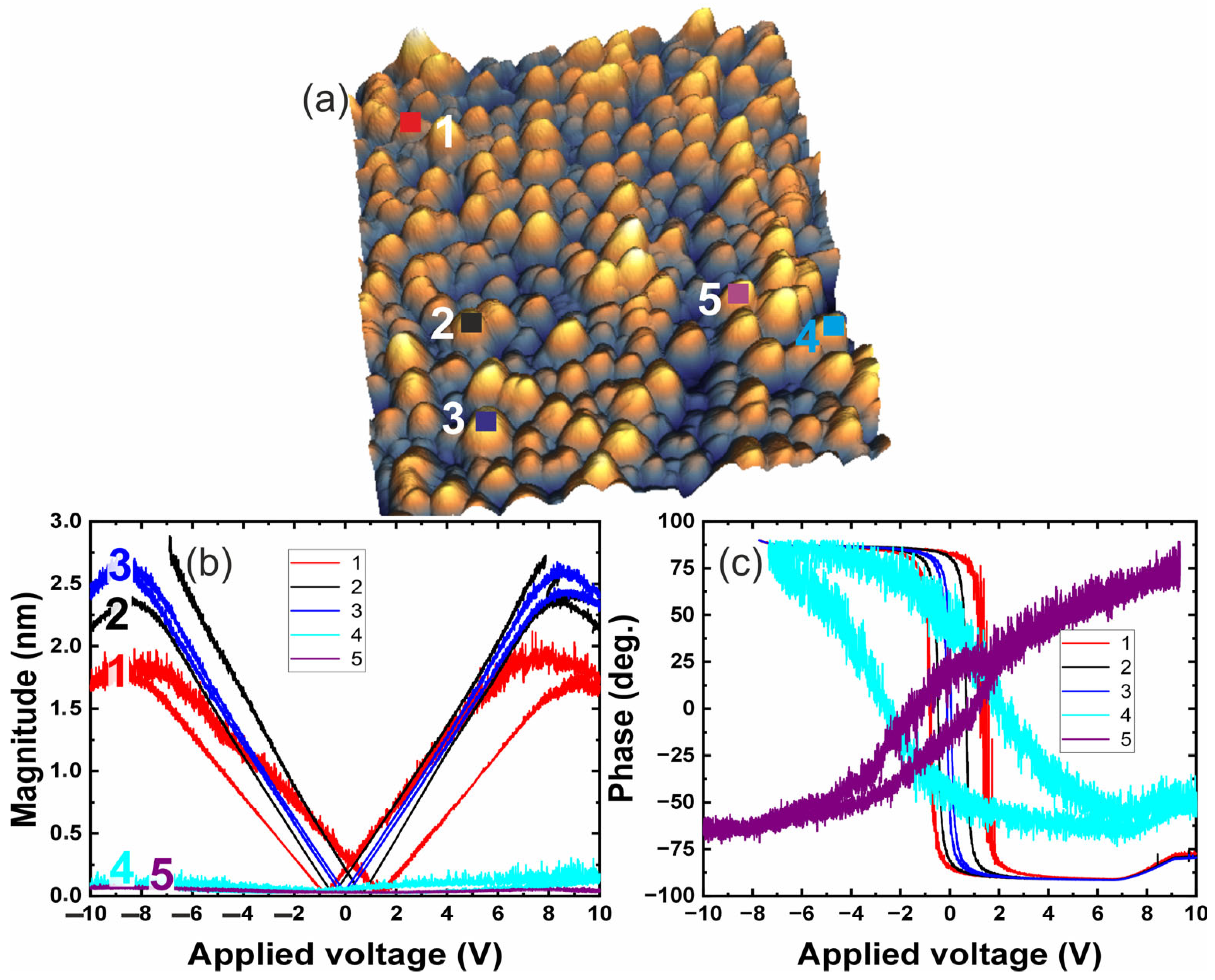
To perform PFM measurements, samples with 0%, 6.6%, and 14% PVP were selected. The 0% PVP sample was chosen as the most densely packed structure, as it was expected to exhibit the most uniform response. In contrast, the 6.6% and 14% PVP samples, due to their unique pore distribution, were anticipated to demonstrate distinct local properties compared to dense structures with the same chemical composition [32]. The PFM method was also being employed to obtain and analyze the distribution of the local piezoelectric hysteresis loops on the samples’ surfaces. During scanning, two signals were recorded: cantilever deflection from its initial position, which characterized piezoelectric deformation in response to the applied field (the magnitude of PFM signal), and the shift in cantilever vibration frequency relative to the lock-in detector frequency, indicating the direction of deformation (the phase of PFM signal). The phase signal was used to determine polarization, as in ferroelectric structures, there is a direct linear correlation between piezoelectric deformation and polarization. This method provided insight into the local piezoelectric properties of the samples and how they are influenced by the presence of porosity and structural heterogeneity.
Figure 4 presents the local piezoelectric hysteresis loops for the 0% PVP sample. Figure 4a illustrates the scanned area, where different colors indicate contact regions between the probe and the surface of the structure. To ensure experimental accuracy, various grains were selected, with their boundaries marked by white dashed lines. Figure 4b,c depict the piezoelectric deformation (magnitude) response and phase switching as functions of the applied electric field, respectively. While the signal measured in magnitude of hysteresis loops is driven by the thin film-associated electromechanical response, the phase represents the switching behavior of the film. The colors of the curves correspond to the colored squares in the topography image. The results indicate that the dense 0% PVP sample exhibits piezoelectric responses that are consistent within the measurement uncertainty, suggesting that the material properties remain uniform across different grains. This confirms the expected homogeneity of the dense structure, where the absence of pores minimizes local variations in electromechanical behavior.
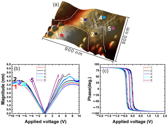
Figure 4.
Local hysteresis loops analysis for the 0% PVP sample, (a) topography of the selected region, where colored squares indicate the probe’s contact points on the surface, (b) magnitude and (c) phase responses of the PFM signal.
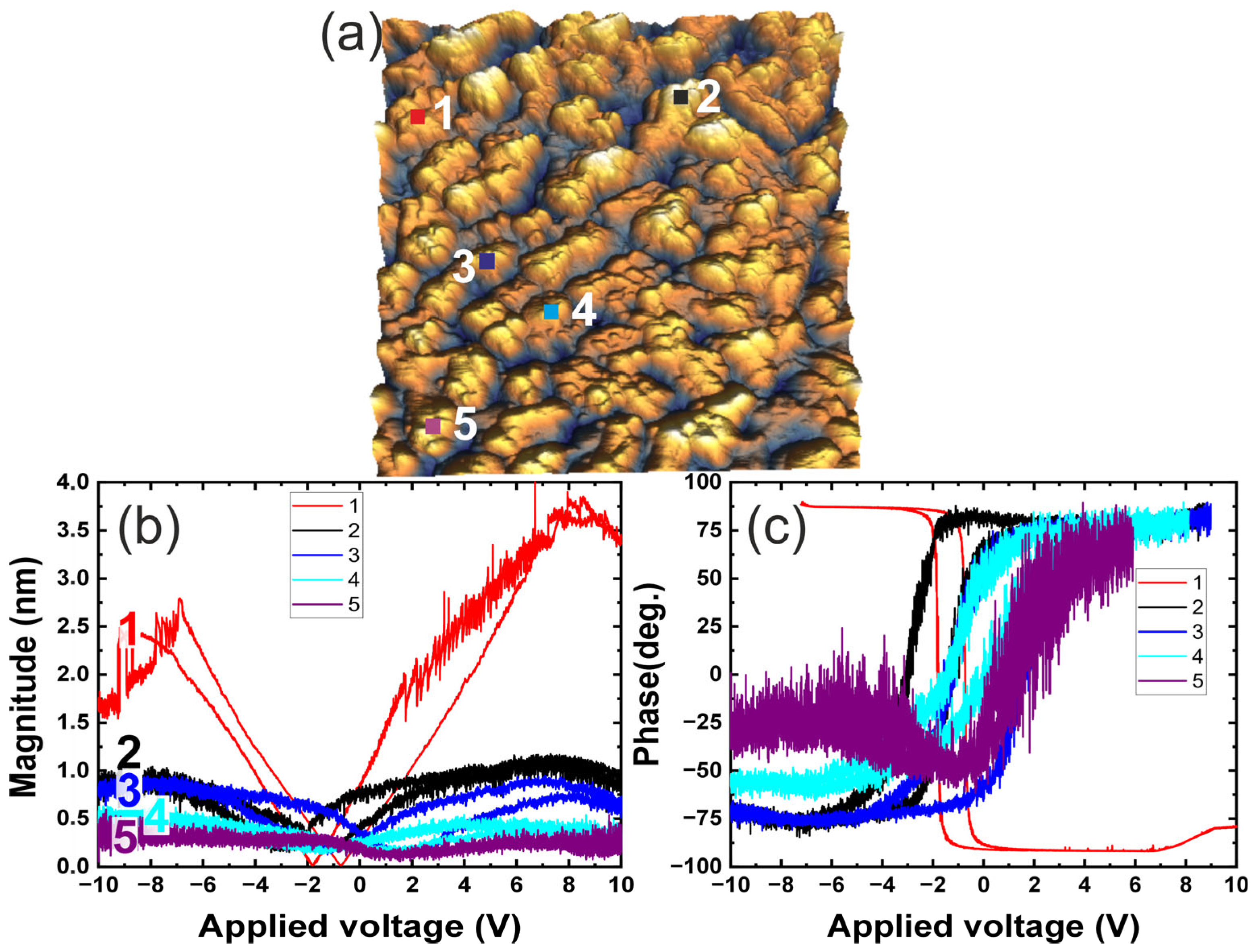
In Figure 5a, the surface is composed of multiple grains, indicating a significant structural transformation compared to the dense 0% PVP sample. These changes in microstructure also introduce distortions in the piezoelectric response dependencies, as observed in Figure 5b,c. Notably, the phase signal hysteresis loop at Point 1 (red line) exhibits a directional change compared to other measurements on this sample, suggesting local variations in ferroelectric behavior. Furthermore, the cantilever deflection due to piezoelectric deformation at Point 1 reaches 3 nm, the highest recorded value, whereas in other cases, the deflection remains below 1 nm.

Figure 5.
Local hysteresis loop analysis for the 6% PVP sample, (a) topography of the selected region 3 × 3 mkm, where colored squares indicate the probe’s contact points on the surface, (b) magnitude and (c) phase responses of the PFM signal.
The surface of the 14% PVP sample consists of distinct, well-defined grains, as shown in Figure 6a. The local piezoelectric hysteresis loops results indicate that the deformation response at Points 1–3 is comparable to that of the dense 0% PVP sample, although slightly lower in magnitude. In contrast, the responses at Points 4 and 5 are more similar to those observed in the 6% PVP sample, as shown in Figure 6b. The polarization hysteresis loops exhibit a similar trend across different measurement points, except for Point 5, where an anomalous response is detected. The change in the loop shape at this location is associated with a low piezoelectric deformation response, below 0.5 nm, which is also observed at Points 4 and 5. However, the mirrored loop reversal, previously identified in the 6% PVP sample, is only present at Point 5 in this case, as shown in Figure 6c. These results suggest that at higher PVP concentrations, the material develops localized electromechanical variations, where some regions retain characteristics of a denser structure, while others behave similarly to more porous configurations.
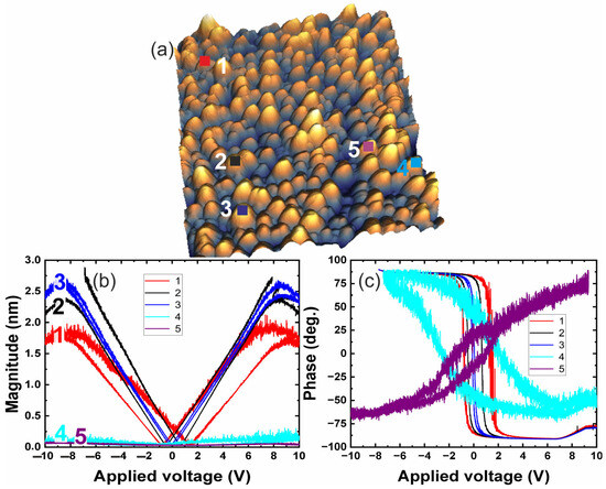
Figure 6.
Local hysteresis loop analysis for the 14% PVP sample, (a) topography of the selected region 3 × 3 mkm, where colored squares indicate the probe’s contact points on the surface, (b) magnitude and (c) phase responses of the PFM signal.
Changes in the magnitude and direction of the polarization hysteresis loops under the applied field were observed exclusively in the 6.6% and 14% PVP samples. The piezoelectric deformation loops of the dense material showed significant differences compared to Points 2–5 in the 6.6% PVP sample and Point 5 in the 14% PVP sample. However, certain cases exhibited no loop reversal (e.g., Point 4 in the 14% PVP sample), yet a more than tenfold reduction in the piezoelectric deformation signal was still observed. These results suggest that at higher PVP concentrations, the structural modifications—particularly the redistribution of charge transport pathways and grain boundary effects—strongly influence the local electromechanical response.
3.5. Analysis of Spontaneous Polarization Distribution Using PFM
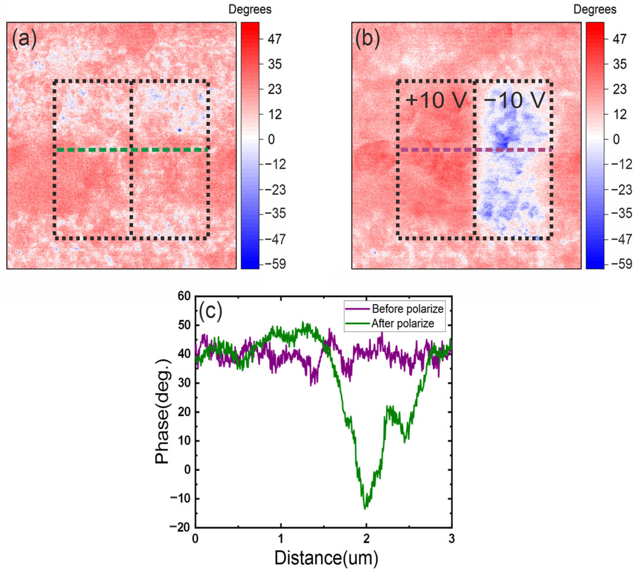
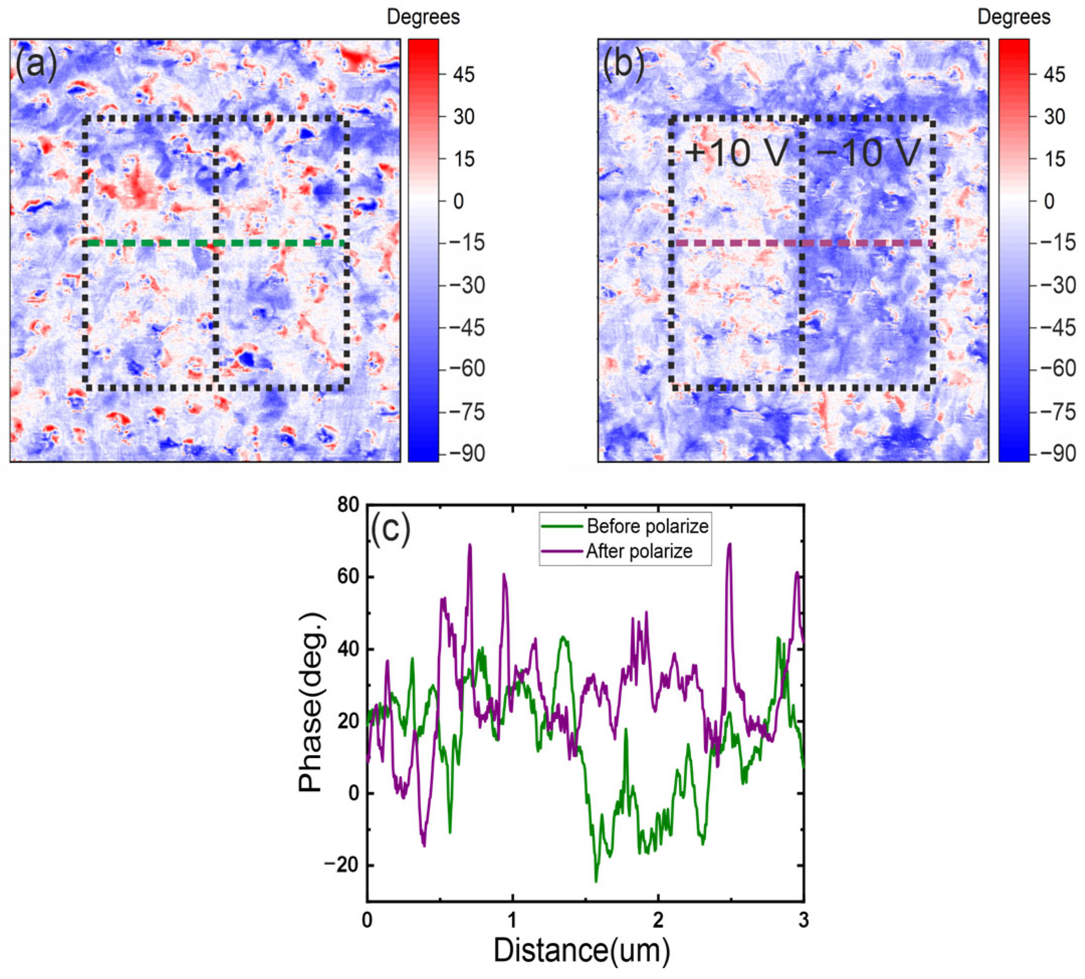
The mapping of spontaneous polarization distribution was performed by applying an alternating electric field to the probe. This study focused on probing the z-component of the signal, meaning only the normal polarization distribution relative to the surface was recorded (out-of-plane PFM). In Figure 7, Figure 8, Figure 9, Figure 10 and Figure 11a,b, the red and blue regions represent two opposite polarization states in the examined ferroelectric films. The blue color indicates a displacement directed outward from the surface, while the red color corresponds to a displacement directed into the film. The white areas in the images represent regions where the beam oscillation phase matches the frequency of the detector oscillations, suggesting minimal or no local polarization contrast.
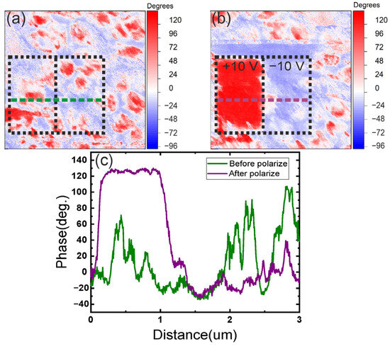
Figure 7.
Cross-section and scanning results of the 3 × 3 mkm polymer-free sample (10 layers of PZT, thickness 370 nm, 0% porosity), (a) polarization contrast before repolarization, showing the initial distribution of spontaneous polarization, (b) polarization contrast after repolarization, illustrating the effect of charge lithography on the ferroelectric domain structure, (c) cross-section along the scan width, highlighting polarization variations before and after repolarization.
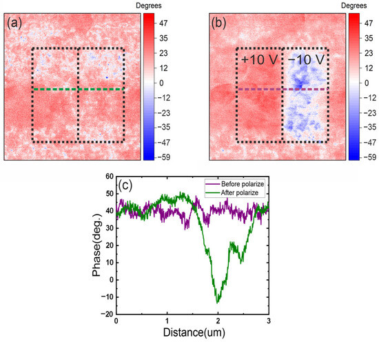
Figure 8.
Cross-section and scanning results of the 3 × 3 mkm 1% PVP sample (9 layers of PZT, thickness 390 nm, 6.8% porosity), (a) polarization contrast before repolarization, illustrating the initial spontaneous polarization distribution in the porous structure, (b) polarization contrast after repolarization, showing the altered domain structure and its weaker response to charge lithography, (c) cross-section along the scan width, highlighting polarization variations before and after repolarization.
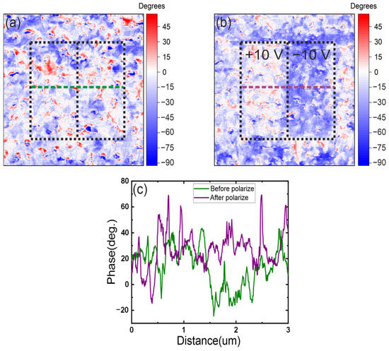
Figure 9.
Cross-section and scanning results of the 3 × 3 mkm 3% PVP sample (7 layers of PZT, thickness 370 nm, 11% porosity), (a) polarization contrast before repolarization, illustrating the initial spontaneous polarization distribution and the increased influence of porosity on domain formation, (b) polarization contrast after repolarization, demonstrating the irregular and less stable polarization switching due to enhanced porosity, (c) cross-section along the scan width, highlighting polarization variations before and after repolarization.
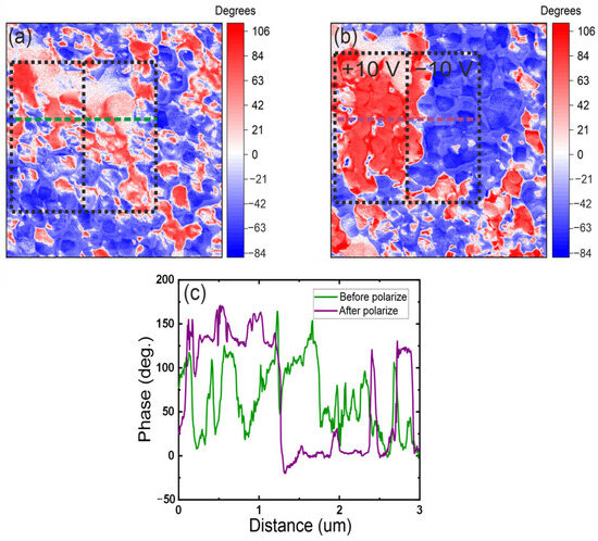
Figure 10.
Cross-section and scanning results of the 3 × 3 mkm 6.6% PVP sample (4 layers of PZT, thickness 390 nm, 33.3% porosity), (a) polarization contrast before repolarization, showing the domain structure and polarization distribution in a highly porous film, (b) polarization contrast after repolarization, demonstrating the material’s response to charge lithography and the effectiveness of polarization switching, (c) cross-section along the scan width, illustrating the variations in polarization response and the influence of increased porosity on domain alignment.
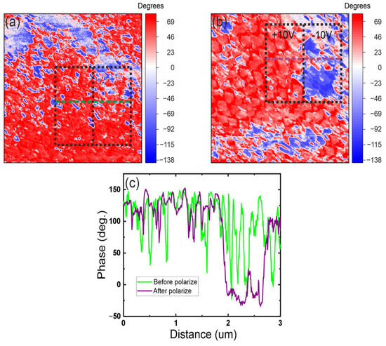
Figure 11.
Cross-section and scanning results of the 3 × 3 mkm 14% PVP sample (3 layers of PZT, approximate thickness 400 nm, porosity not measured), (a) polarization contrast before repolarization, showing the domain structure and polarization distribution in a highly porous film, (b) polarization contrast after repolarization, demonstrating the material’s response to charge lithography and the effectiveness of polarization switching, (c) cross-section along the scan width, illustrating the variations in polarization response and the influence of increased porosity on domain alignment.
The predominance of the blue color in the initial polarization state, observed before the polarization process, indicates that negatively polarized domains dominate over positively polarized ones. To modify the polarization distribution profiles, charge lithography was employed. During this process, voltages of opposite polarity were applied to the left and right sides of the mask. As a result, within the masked area, a red region was induced by the application of a positive voltage, while a blue region emerged due to the application of a negative voltage. This demonstrates the reversibility of polar states under the influence of an external electric field. The external areas in the images represent the initial piezoresponse of the films before polarization modification, highlighting the contrast between the pristine and electrically manipulated states.
The modification of ferroelectric materials inevitably leads to changes in their polarization characteristics. This effect was previously demonstrated in the topography analysis, where the addition of polymer altered the material’s surface morphology. For further analysis of the polarization images obtained using PFM, the scanning data from the polymer-free sample are used as a reference standard. These baseline measurements serve as a benchmark for comparison and normalization of the polarization response before and after the repolarization process. By utilizing this approach, it is possible to quantify the influence of polymer-induced porosity on the local polarization states and assess how structural modifications affect the ferroelectric switching behavior.
Figure 7a presents the piezoresponse mapping of the polymer-free sample, showing the initial polarization state across the surface. The corresponding image in Figure 7b demonstrates that the structure undergoes effective repolarization following the applied charge lithography mask. To further assess the polarization state before and after repolarization, a cross-sectional analysis along the entire scan width was performed (Figure 7c). Despite the presence of surface irregularities, the results indicate that these variations do not significantly affect the polarization process. Although PFM cannot directly determine the absolute polarization vector orientation, it enables the calculation of frequency shifts in cantilever oscillations relative to the lock-in detector frequency during scanning. This provides insight into the direction of deformation—either inward or outward—relative to the surface normal. Due to the inverse relationship between piezoelectric deformation direction and the polarization vector, these measurements allow for the effective evaluation of polarization distribution. Based on the cross-sectional analysis, the maximum polarization response was determined to be 127° for the positive orientation and 33° for the negative orientation.
As previously noted, the introduction of 1% PVP results in the formation of pores on the sample surface. Figure 8a presents the spontaneous polarization distribution map for the 1% PVP sample, illustrating the altered domain structure compared to the dense reference sample. The piezoresponse mapping for negative segments appears fragmented, with a noticeable lack of strong alignment with the charge lithography mask (Figure 8b). This suggests that the presence of porosity disrupts the uniformity of polarization switching, likely due to local charge trapping or altered domain wall motion. A significant reduction in the maximum polarization response is observed in this sample. The maximum response for positive polarization is measured at 51°, which is 2.5 times lower than in the reference (polymer-free) sample. Similarly, the response for negative domains also decreases, reaching only 13°, as shown in Figure 8c. These findings indicate that even a small concentration of PVP (1%) significantly affects polarization behavior, weakening the piezoresponse and reducing the effectiveness of domain reorientation under an external electric field.
The total porosity of the 3% PVP sample increased by 4.2% compared to the previous (1% PVP) sample. This difference significantly impacts the formation of domains and the distribution of spontaneous polarization, as illustrated in Figure 9a. A noticeable increase in pore concentration on the surface further alters the material’s electromechanical response. The increased porosity likely enhances conductivity, leading to a more chaotic polarization process, as seen in Figure 9b. This disruption is attributed to the presence of additional grain boundaries and charge accumulation effects, which interfere with uniform domain switching. The maximum piezoresponse for positive domains was measured at 51°, while for negative domains, it increased to 26°, as shown in Figure 9c. This suggests that while polarization switching is still achievable, the overall response remains weaker and more irregular than in the denser reference samples.
The PFM image presented in Figure 10a for the 6.6% PVP sample reveals that the overall domain distribution and spatial coverage of regions polarized in the same direction resemble those observed in a dense film. A similar trend is evident in the charge lithography process, as shown in Figure 10b. Despite structural similarities, the air-phase area (porous space) has increased by 2.6 times compared to the polymer-free sample. These findings suggest that structures with specific grain orientation may exhibit a more efficient response to external electric stimuli, potentially due to the alignment of polarization switching pathways within the material. The maximum piezoresponse measured for positive domains was 171°, while for negative domains, it reached 45°, as shown in Figure 10c.
The air-phase area in the analyzed region of the 14% PVP sample is 1.6 μm2, which is comparable to the porous area in the 3% PVP sample. This similarity can be attributed to the possibility of grains being embedded within the pores, which reduces the fragmentation of the overall polarization response, as shown in Figure 11a. Due to the smaller grain sizes and the preferential distribution of the electric field along their edges, a misalignment with the expected polarization pattern is observed, as depicted in Figure 11b. The maximum piezoresponse for positive domains reached 152°, while for negative domains, it was 33°, as shown in Figure 11c. These results indicate that at higher PVP concentrations, the polarization response becomes less disrupted despite increased porosity.
The decay of the squares deposited by charge lithography from sample to sample is due to the increase in the porosity of the material caused by an increase in the PVP concentration. This porosity leads to fragmentation of the domain structure, disruption of grain boundaries, and non-uniform polarization distribution. Local variations in the domain distribution caused by grain boundary disruption in porous samples negatively affect the stability and uniformity of the piezoelectric response, which leads to a decline in the quality and clarity of the squares created by charge lithography. We found that an increase in porosity, caused by a high PVP content, leads to fragmentation of the domain structure and a nonuniform distribution of polarization. When comparing the results for 0% PVP film, a strong correlation is observed with the study by Feigl et al. [37], which investigated the manipulation of charged domain walls in ferroelectric multilayers. The experiment, utilizing piezoresponse force microscopy (PFM) for local polarization switching, demonstrated significant control capabilities. The study revealed that applying bias via the PFM probe enables precise modulation of both in-plane and out-of-plane polarization components. This controlled manipulation results in the formation of secondary domains and associated charged domain walls within the ferroelectric structure, consistent with switching mechanisms in tetragonal systems. Further expanding on the relationship between porosity and domain behavior, another investigation explored the microstructural evolution and domain engineering in porous PZT thin films [25]. This research systematically assessed how varying porosity impacts spontaneous polarization and electromechanical response, with PFM serving as a key tool for visualizing domain structures. The findings indicate that increased porosity leads to a decrease in remnant polarization and saturation polarization, primarily due to the reduction in the fraction of active ferroelectric material and the introduction of depolarization fields around the pores. The disruption of the grain boundaries in the porous samples results in local variations in domain distribution, which negatively affects the stability and uniformity of the piezoelectric response. In contrast, in the work by Cornelius et al. [37], the films produced by the sol–gel method exhibit a more stable and uniformly oriented domain structure, despite the presence of an imprint effect. PFM images demonstrate a consistent distribution of polarization domains, which results in high effective d33eff values. Moreover, the dependence of d33eff on the measurement direction (e.g., [100] vs. [110]) and the observed asymmetry between the values for positive and negative electric fields indicate that the optimized microstructure promotes a more reliable and uniform piezoelectric response.
4. Conclusions
The electrophysical mechanisms governing spontaneous polarization in ferroelectric materials play a crucial role in determining their functional properties. Unlike porous ferroelectric materials, where the presence of pores introduces inhomogeneities in the electric field distribution, dense ferroelectric films lack such variations, resulting in a more uniform polarization response. A key factor influencing this behavior is the relative dielectric permittivity of the air phase, which is significantly lower than that of the ferroelectric film. As a result, increasing porosity leads to a thicker film, a reduction in dielectric permittivity, and a decrease in overall polarization. Despite these changes, an important observation is that the local coercive field remains largely unchanged, suggesting a relative stability in the material’s resistance to polarization switching. The internal field, generated by internal charge displacement, can be oriented in both positive and negative directions, potentially leading to either polarization or depolarization effects. In the case of the samples studied, the source of this internal field is the interaction between dipole structures, which are confined by specific interfaces and geometrical constraints. These interactions dictate the local stability and switching behavior of the polarization, further emphasizing the complex role of microstructure and porosity in shaping the electromechanical properties of ferroelectric materials.
Author Contributions
Conceptualization., A.B. and M.I.; methodology, E.Z.; software, E.Z.; validation, E.Z., A.B. and D.S.; formal analysis, A.B. and D.S.; investigation, E.Z.; resources, A.B.; data curation, D.S.; writing—original draft preparation, E.Z. and A.B.; writing—review and editing, A.B. and M.I.; visualization, E.Z. and D.S.; supervision, A.B. and M.I.; project administration, A.B. and D.S.; funding acquisition, A.B. All authors have read and agreed to the published version of the manuscript.
Funding
The experimental research using AFM and PFM methods was supported by the Russian Science Foundation, Project No.24-79-10304, https://rscf.ru/en/project/24-79-10304/ (accessed on September 2024–May 2025). The preparation of PZT samples was supported by the Ministry of Science and Higher Education of the Russian Federation (State Task for the University #FSFZ-2023-0005).
Data Availability Statement
The research data are available upon request.
Acknowledgments
M.I. thanks “ILLIANCE” project supported by the PRR—Recovery and Resilience Plan and by NextGenerationEU, through the scheme «Agendas para a Inovação Empresarial» and CICECO-Aveiro Institute of Materials, UIDB/50011/2020 (DOI 10.54499/UIDB/50011/2020), UIDP/50011/2020 (DOI 10.54499/UIDP/50011/2020) and LA/P/0006/2020 (DOI 10.54499/LA/P/0006/2020), financed by national funds through the FCT/MCTES (PIDDAC). The authors also thank Daniil Abdulaev for performing SEM measurements and Andrey Elshin for conducting XRD measurements.
Conflicts of Interest
The authors declare no conflicts of interest.
References
- Bi, K.; Han, S.; Chen, J.; Bi, X.; Yang, X.; Niu, L.; Mei, L. Interfacial Polarization Control Engineering and Ferroelectric PZT/Graphene Heterostructure Integrated Application. Nanomaterials 2024, 14, 432. [Google Scholar] [CrossRef]
- Sezer, N.; Koç, M. A comprehensive review on the state-of-the-art of piezoelectric energy harvesting. Nano Energy 2021, 80, 105567. [Google Scholar] [CrossRef]
- Li, X.; Wang, K.; Wang, Y.L.; Wang, K.C. Plantar pressure measurement system based on piezoelectric sensor: A review. Sens. Rev. 2022, 42, 241–249. [Google Scholar] [CrossRef]
- Jung, J.; Lee, W.; Kang, W.; Shin, E.; Ryu, J.; Choi, H. Review of piezoelectric micromachined ultrasonic transducers and their applications. J. Micromech. Microeng. 2017, 27, 113001. [Google Scholar] [CrossRef]
- Saadon, S.; Sidek, O. A review of vibration-based MEMS piezoelectric energy harvesters. Energy Convers. Manag. 2011, 52, 500–504. [Google Scholar] [CrossRef]
- Duan, S.; Wu, J.; Xia, J.; Lei, W. Innovation Strategy Selection Facilitates High-Performance Flexible Piezoelectric Sensors. Sensors 2020, 20, 2820. [Google Scholar] [CrossRef]
- Fedulov, F.A.; Saveliev, D.V.; Chashin, D.V.; Shishkin, V.I.; Fetisov, Y.K. Magnetoelectric effects in stripe- and periodic heterostructures based on nickel–lead zirconate titanate bilayers. Russ. Technol. J. 2022, 10, 64–73. [Google Scholar] [CrossRef]
- Yan, M.; Xiao, Z.; Ye, J.; Yuan, X.; Li, Z.; Bowen, C.; Zhang, Y.; Zhang, D. Porous ferroelectric materials for energy technologies: Current status and future perspectives. Energy Environ. Sci. 2021, 14, 6158–6190. [Google Scholar] [CrossRef]
- Fei, C.; Chen, Z.; Fong, W.M.; Zhu, B.; Wang, L.; Ren, W.; Li, Y.; Shi, J.; Shung, K.K.; Zhou, Q. Modification of microstructure on PZT films for ultrahigh frequency transducer. Ceram. Int. 2015, 41, S650–S655. [Google Scholar] [CrossRef] [PubMed]
- Atanova, A.V.; Zhigalina, O.M.; Khmelenin, D.N.; Orlov, G.A.; Seregin, D.S.; Sigov, A.S.; Vorotilov, K.A. Microstructure analysis of porous lead zirconate–titanate films. J. Am. Ceram. Soc. 2021, 105, 639–652. [Google Scholar] [CrossRef]
- Zhang, S.; Li, F.; Jiang, X.; Kim, J.; Luo, J.; Geng, X. Advantages and challenges of relaxor-PbTiO3 ferroelectric crystals for electroacoustic transducers—A review. Prog. Mater. Sci. 2015, 68, 1–66. [Google Scholar] [CrossRef]
- Xiao, W.; Chen, Z.; Liu, X.; Zhou, Z.; Fu, Z.; Tang, Y.; Liang, R. Well-balanced performance achieved in PZT piezoceramics via a multiscale regulation strategy. Mater. Horiz. 2024, 11, 5285–5294. [Google Scholar] [CrossRef]
- Liu, H.; Lin, X.; Zhang, S.; Huan, Y.; Huang, S.; Cheng, X. Enhanced performance of piezoelectric composite nanogenerator based on gradient porous PZT ceramic structure for energy harvesting. J. Mater. Chem. A 2020, 8, 19631–19640. [Google Scholar] [CrossRef]
- Zhang, Y.; Bao, Y.; Zhang, D.; Bowen, C.R. Porous PZT Ceramics with Aligned Pore Channels for Energy Harvesting Applications. J. Am. Ceram. Soc. 2015, 98, 2980–2983. [Google Scholar] [CrossRef]
- Zhang, Y.; Xie, M.; Roscow, J.; Bao, Y.; Zhou, K.; Zhang, D.; Bowen, C.R. Enhanced pyroelectric and piezoelectric properties of PZT with aligned porosity for energy harvesting applications. J. Mater. Chem. A 2017, 5, 6569–6580. [Google Scholar] [CrossRef]
- Jia, Q.X.; McCleskey, T.M.; Burrell, A.K.; Lin, Y.; Collis, G.E.; Wang, H.; Li, A.D.Q.; Foltyn, S.R. Polymer-assisted deposition of metal-oxide films. Nat. Mater. 2004, 3, 529–532. [Google Scholar] [CrossRef]
- Kozuka, H.; Takenaka, S.; Tokita, H.; Okubayashi, M. PVP-assisted sol-gel deposition of single layer ferroelectric thin films over submicron or micron in thickness. J. Eur. Ceram. Soc. 2004, 24, 1585–1588. [Google Scholar] [CrossRef]
- Yamano, A.; Takata, K.; Kozuka, H. Ferroelectric domain structures of 0.4-μm-thick Pb(Zr,Ti)O3 films prepared by polyvinylpyrrolidone-assisted Sol-Gel method. J. Appl. Phys. 2012, 111, 054109. [Google Scholar] [CrossRef]
- Stancu, V.; Lisca, M.; Boerasu, I.; Pintilie, L.; Kosec, M. Effects of porosity on ferroelectric properties of Pb(Zr0.2Ti0.8)O3 films. Thin Solid Film. 2007, 515, 6557–6561. [Google Scholar] [CrossRef]
- Oh, S.-M.; Kang, M.-G.; Do, Y.-H.; Kang, C.-Y.; Yoon, S.-J.; Nahm, S. Fabrication of 1 μm Thickness Lead Zirconium Titanate Films Using Poly(N-vinylpyrrolidone) Added Sol-gel Method. Trans. Electr. Electron. Mater. 2011, 12, 222–225. [Google Scholar] [CrossRef]
- Yang, A.; Wang, C.; Guo, R.; Huang, Y. Microstructure and Electrical Properties of Porous PZT Ceramics Fabricated by Different Methods. J. Am. Ceram. Soc. 2010, 93, 1984–1990. [Google Scholar] [CrossRef]
- Björk, E.M. Surface Area Determination of Particle-Based Mesoporous Films Using Krypton Physisorption. ACS Omega 2024, 9, 5899–5902. [Google Scholar] [CrossRef]
- Choi, J.-J.; Park, G.-T.; Lee, S.-M.; Kim, H.-E. Sol–Gel Preparation of Thick PZN–PZT Film Using a Diol-Based Solution Containing Polyvinylpyrrolidone for Piezoelectric Applications. J. Am. Ceram. Soc. 2005, 88, 3049–3054. [Google Scholar] [CrossRef]
- Wang, Q.; He, S.; Bowen, C.R.; Xiao, X.; Oh, J.A.S.; Sun, J.; Zeng, K.; Lei, W.; Chen, J. Porous pyroelectric ceramic with carbon nanotubes for high-performance thermal to electrical energy conversion. Nano Energy 2022, 102, 107703. [Google Scholar] [CrossRef]
- Schultheiß, J.; Roscow, J.I.; Koruza, J. Orienting anisometric pores in ferroelectrics: Piezoelectric property engineering through local electric field distributions. Phys. Rev. Mater. 2019, 3, 084408. [Google Scholar] [CrossRef]
- Zhang, Y.; Roscow, J.; Lewis, R.; Khanbareh, H.; Topolov, V.Y.; Xie, M.; Bowen, C.R. Understanding the effect of porosity on the polarisation-field response of ferroelectric materials. Acta Mater. 2018, 154, 100–112. [Google Scholar] [CrossRef]
- Du, Z.H.; Ma, J. The effect of PVP on the critical thickness and properties of PLZT ceramic films. J. Electroceram. 2006, 16, 565–569. [Google Scholar] [CrossRef]
- Saegusa, T.; Chujo, Y. Organic-inorganic polymer hybrids. Makromolekulare Chemie. Macromol. Symp. 1992, 64, 11–19. [Google Scholar]
- Roscow, J.; Zhang, Y.; Taylor, J.; Bowen, C. Porous ferroelectrics for energy harvesting applications. Eur. Phys. J. Spec. Top. 2015, 224, 2949–2966. [Google Scholar] [CrossRef]
- Ivanov, M.; Grempka, A.; Buryakov, A.; Nikitin, T.; Justino, L.L.G.; Fausto, R.; Vilarinho, P.M.; Paixão, J.A. Nanoscale Study of the Polar and Electronic Properties of a Molecular Erbium(III) Complex Observed via Scanning Probe Microscopy. Crystals 2023, 13, 1331. [Google Scholar] [CrossRef]
- Delimova, L.; Seregin, D.; Orlov, G.; Zaitseva, N.; Gushchina, E.; Sigov, A.; Vorotilov, K. Porous PZT Films: How Can We Tune Electrical Properties? Materials 2023, 16, 5171. [Google Scholar] [CrossRef] [PubMed]
- Zheng, X.; Li, J.; Zhou, Y. X-ray diffraction measurement of residual stress in PZT thin films prepared by pulsed laser deposition. Acta Mater. 2004, 52, 3313–3322. [Google Scholar] [CrossRef]
- Park, G.-T.; Choi, J.-J.; Park, C.-S.; Lee, J.-W.; Kim, H.-E. Piezoelectric and ferroelectric properties of 1-μm-thick lead zirconate titanate film fabricated by a double-spin-coating process. Appl. Phys. Lett. 2004, 85, 2322–2324. [Google Scholar] [CrossRef]
- Rodríguez-Aranda, M.C.; Calderón-Piñar, F.; Espinoza-Beltrán, F.J.; Flores-Ruiz, F.J.; León-Sarabia, E.; Mayén-Mondragón, R.; Yáñez-Limón, J.M. Ferroelectric hysteresis and improved fatigue of PZT (53/47) films fabricated by a simplified sol–gel acetic-acid route. J. Mater. Sci. Mater. Electron. 2014, 25, 4806–4813. [Google Scholar] [CrossRef]
- Nguyen, M.D.; Houwman, E.P.; Rijnders, G. Large piezoelectric strain with ultra-low strain hysteresis in highly c-axis oriented Pb(Zr0.52Ti0.48)O3 films with columnar growth on amorphous glass substrates. Sci. Rep. 2017, 7, 12915. [Google Scholar] [CrossRef]
- Feigl, L.; Sluka, T.; McGilly, L.J.; Crassous, A.; Sandu, C.S.; Setter, N. Controlled creation and displacement of charged domain walls in ferroelectric thin films. Sci. Rep. 2016, 6, 31323. [Google Scholar] [CrossRef]
- Cornelius, T.W.; Mocuta, C.; Escoubas, S.; Merabet, A.; Texier, M.; Lima, E.C.; Araujo, E.B.; Kholkin, A.L.; Thomas, O. Piezoelectric response and electrical properties of Pb(Zr1-xTix)O3 thin films: The role of imprint and composition. J. Appl. Phys. 2017, 122, 164104. [Google Scholar] [CrossRef]


Disclaimer/Publisher’s Note: The statements, opinions and data contained in all publications are solely those of the individual author(s) and contributor(s) and not of MDPI and/or the editor(s). MDPI and/or the editor(s) disclaim responsibility for any injury to people or property resulting from any ideas, methods, instructions or products referred to in the content. |
© 2025 by the authors. Licensee MDPI, Basel, Switzerland. This article is an open access article distributed under the terms and conditions of the Creative Commons Attribution (CC BY) license (https://creativecommons.org/licenses/by/4.0/).