Article

Epitaxial Growth of Ni-Mn-Ga on Al2O3(112¯0) Single-Crystal Substrates by Pulsed Laser Deposition

by
Manuel G. Pinedo-Cuba
1,*,
José M. Caicedo-Roque
2,
Jessica Padilla-Pantoja
2,
Justiniano Quispe-Marcatoma
1,
Carlos V. Landauro
1,
Víctor A. Peña-Rodríguez
1 and
José Santiso
2
1
Facultad de Ciencias Físicas, Universidad Nacional Mayor de San Marcos, Lima 15081, Peru
2
Catalan Institute of Nanoscience and Nanotechnology (ICN2), CSIC and BIST, Campus UAB, Bellaterra, 08193 Barcelona, Spain
*
Author to whom correspondence should be addressed.
Surfaces 2025, 8(2), 35; https://doi.org/10.3390/surfaces8020035
Submission received: 14 April 2025 / Revised: 27 May 2025 / Accepted: 28 May 2025 / Published: 30 May 2025
(This article belongs to the Special Issue Surface Engineering of Thin Films)

Abstract

:
Magnetic shape memory alloys have attracted considerable attention due to their multifunctional properties. Among these materials, Ni-Mn-Ga alloys are distinguished by their ability to achieve up to 10% strain when exposed to a magnetic field, a characteristic predominantly observed in single-crystal samples. Consequently, it is essential to develop nanomaterials with a crystal structure closely resembling that of a single crystal. In this study, an epitaxial Ni-Mn-Ga thin film was fabricated using Pulsed Laser Deposition on an Al2O3  ( 11 2 ¯ 0 ) single-crystal substrate. The crystal structure was characterised through X-ray diffraction methodologies, such as symmetrical 2 θ ω scans, pole figures, and reciprocal space maps. The results indicated that the sample was mainly in a slightly distorted cubic austenite phase, and some incipient martensite phase also appeared. A detailed microstructural analysis, performed by transmission electron microscopy, confirmed that certain regions of the sample exhibited an incipient transformation to the martensite phase. Regions closer to the substrate retained the austenite phase, suggesting that the constraint imposed by the substrate inhibits the phase transition. These results indicate that it is possible to grow high crystalline quality thin films of Ni-Mn-Ga by Pulsed Laser Deposition.

1. Introduction

Magnetic shape memory alloys (MSMAs) exhibit multifunctional properties, making them suitable for applications such as transducers, actuators, sensors, microelectromechanical systems (MEMS), and magnetic refrigerators [1]. The primary characteristic of MSMAs is their magnetic-field-induced strain (MFIS), which refers to the generation of internal strains in response to an external magnetic field. This property is particularly relevant for the next generation of sensing and actuating devices, as MSMAs offer higher recoverable strain and faster response time compared to existing technologies [2]. Magnetic actuation in MSMAs occurs through two distinct mechanisms: magnetically induced reorientation of martensite variants [3] and field-induced martensitic transition [4]. In the first mechanism, the rearrangement of martensite variants is governed by the high magnetocrystalline anisotropy energy of the martensite phase and the low twinning stress between martensite variants. When an external magnetic field reorients the variants, microstructural changes result in significant strain. The second mechanism, field-induced martensitic transition, takes place due to a shift in the transition temperature caused by the applied magnetic field. This temperature variation can be approximately described by the Clausius–Clapeyron relation and is observed when a substantial difference in magnetisation exists between the phases (e.g., one being ferromagnetic and the other antiferromagnetic). However, this effect requires the application of high magnetic fields, typically in the range of several Teslas. While this mechanism generally produces greater strain than the first, its practical implementation in commercial devices is limited by the necessity of strong magnetic fields. Consequently, magnetically induced reorientation of martensite variants, which can typically be achieved with fields below 1 T, is considered more suitable for the development of new devices [5].
The Heusler alloy Ni2MnGa is the most representative MSMA due to its large MFIS values [3,6]. Sozinov et al. [7] reported a record MFIS of nearly 10% in single crystals at room temperature under an applied magnetic field of less than 1 T. In contrast, polycrystalline Ni-Mn-Ga exhibits significantly lower MFIS values, around 0.3%, which, although reduced compared to single crystals, remain higher than those of commercial NiTi-based MSMAs. This reduction in MFIS is attributed to the inhibition of twin boundary motion by constraints imposed by grain boundaries [8]. However, through structural engineering (specifically, the introduction of pores smaller than the grain size), these constraints can be mitigated, leading to a substantial increase in MFIS to values ranging from 2.0% to 8.7% [9]. This further supports the intrinsic correlation between MFIS and the crystalline microstructure. Typically, stoichiometric Ni2MnGa alloy crystallises in a high-temperature phase known as austenite. This phase is characterised by a cubic crystal structure with space group 225, where the atomic Wyckoff positions of Ni, Mn, and Ga are 8 c ( 1 / 4 , 1 / 4 , 1 / 4 ) , 4 a ( 0 , 0 , 0 ) , and 4 b ( 1 / 2 , 1 / 2 , 1 / 2 ) , respectively (also referred to as the L21 structure). However, as the temperature decreases, austenite becomes unstable and undergoes a martensitic phase transition. The resulting martensite phase emerges through a distortion of the austenite unit cell along the crystallographic 001 A directions, leading to tetragonal, orthorhombic, or triclinic unit cells. Due to the coexistence of austenite and martensite during the phase transition, significant elastic energy arises from the mismatch between their lattice parameters. To minimise this elastic energy, the martensite phase undergoes periodic shuffling along the ( 110 ) A planes in the [ 1 1 ¯ 0 ] direction, forming structural modulations [10]. These modulations result in a complex crystalline structure that can be described as a superstructure composed of shuffled ( 110 ) A planes. The most common martensitic structures observed in Ni2MnGa include five modulated (5M), seven modulated (7M), and non-modulated (NM) phases [11,12]. In single crystals, the crystal structure of the martensite phase has been found to be a key factor in determining the observed MFIS values. Typical MFIS values of 5–7% have been achieved in 5M martensite, while higher values, around 10%, have been reported for 7M. In contrast, NM martensite exhibits negligible MFIS [13]. The maximum allowed twinning strain ( ε 0 = | 1 c / a | ) is strictly dependent on the crystal lattice parameters. However, despite having the highest ε 0 value, NM martensite does not exhibit significant MFIS. This behaviour is attributed to its high twinning stress, which restricts twin boundary motion under an applied magnetic field. For twin boundary motion to occur, the twinning stress must be lower than the maximum magnetic stress, given by σ m a g = K u / ε 0 , where K u is the magnetocrystalline anisotropic energy density. Conversely, the 5M and 7M martensitic structures are formed through a twinning process from an NM structure, aimed at reducing magnetoelastic energy associated with twin boundary stress [14]. As a result, 5M and 7M martensites exhibit lower twinning stress, allowing for significant MFIS. The difference in MFIS values between the 5M and 7M structures is primarily attributed to the maximum ε 0 value dictated by their respective structures.
Despite its remarkable properties, bulk Ni2MnGa is brittle, which limits its technological applications. To harness its large MFIS values in practical applications, improving its ductility is essential to prevent fracture under repeated operations. Various processing approaches have been explored to enhance its mechanical properties [15], with size reduction being the most widely used strategy [16]. In the case of thin films, high crystalline quality—comparable to that of single crystals—can be achieved through epitaxial growth, characterised by a low density of grain boundaries. Physical vapour deposition (PVD) techniques are commonly employed to produce such films. However, achieving high crystallinity requires fulfilling specific conditions, including sufficient atomic mobility upon arrival at the substrate and adequate time for atoms to reach their equilibrium positions. Several PVD techniques meet these requirements, including magnetron sputtering, Pulsed Laser Deposition (PLD), and molecular beam epitaxy (MBE). Among these, magnetron sputtering offers higher growth rates, making it the most widely used method for the deposition of epitaxial Ni-Mn-Ga thin films [17,18,19,20,21]. Extensive studies have investigated different growth parameters and single-crystal substrates to optimise crystallinity and achieve MFIS response [19,21]. In contrast, the growth of Ni-Mn-Ga films via PLD is less common, even though the PLD process offers a wider operational pressure range compared to magnetron sputtering, which is limited by plasma pressure. Tello et al. [22] successfully grew polycrystalline Ni-Mn-Ga films by PLD using single-crystalline Ni-Mn-Ga targets. Similarly, Hakola et al. [23] demonstrated the deposition of polycrystalline Ni-Mn-Ga films on silicon substrates from a polycrystalline target. In a comparative study of RF sputtering and PLD, Zhang et al. [24] demonstrated that PLD enables epitaxial growth on MgO substrates, highlighting its potential for high-quality film deposition. These findings underscore the need for further exploration of PLD growth conditions to optimise the epitaxial growth of Ni-Mn-Ga films.
This study demonstrates the feasibility of growing Ni-Mn-Ga epitaxial films on a-cut Al2O3 substrates using PLD. X-ray diffraction (XRD) techniques—including symmetrical 2 θ ω scans, pole figure measurements, and reciprocal space mapping—were employed to identify the austenitic Ni-Mn-Ga phase and to analyse the crystallographic relationship between the substrate and the film. Cross-sectional images obtained by high-resolution scanning transmission electron microscopy (HR-STEM) provide insight into the film microstructure. In addition, HR-STEM images reveal the early formation of the martensitic phase in regions furthest from the film–substrate interface. While further optimisation of the growth parameters remains necessary, the results confirm the potential for epitaxial growth of Ni-Mn-Ga on a-cut Al2O3 substrates by PLD.

2. Materials and Methods

Ni-Mn-Ga (NMG) samples were grown using the PLD technique on various substrate types (see Appendix A). In this work, we focus on the analysis of the optimised sample deposited on an Al2O3  ( 11 2 ¯ 0 ) single-crystal substrate. The film was deposited in a high-vacuum PLD chamber using a commercial Ni48Mn23Ga29 (at.%) target with a 1.5 inch diameter. The target was mounted on a rotating holder operating at 15 rpm to ensure uniform ablation of its surface. The laser pulses were generated by a Lambda Physik COMPex 201 KrF excimer laser, operating at a wavelength of 248 nm and a maximum pulse energy of 750 mJ. A simple lens system with a focal length of 300 mm was employed to focus the beam onto a spot size of approximately 6 mm2 on the target surface. A total of 40,000 laser pulses were applied at a repetition rate of 10 Hz during the deposition. The initial laser fluence was set to 1.7 J/cm2; however, due to progressive coating of the laser lens during ablation, the fluence gradually decreased to 1.1 J/cm2. The deposition was performed under high-vacuum conditions, with a chamber pressure of approximately 2.1 × 10 7 mbar, while the substrate was maintained at a temperature of T = 773 K. Following deposition, the sample was annealed at the same temperature for 1 h to promote crystallinity, and subsequently allowed for the cooling of the room temperature inside the chamber. The final film thickness, as determined by HR-STEM images, was approximately 70 nm.
Scanning Electron Microscopy (SEM) images were acquired using a FEI Quanta 650 FEG Field Emission Scanning Electron Microscope (FEI, Hillsboro, OR, USA), operated at 5 kV for low-magnification imaging and at 20 kV for high-resolution observations. The surface topography of the sample was analysed in tapping mode with an MFP-3D Atomic Force Microscope, AFM, (Asylum Research, Santa Barbara, CA, USA). Structural characterisation was performed at room temperature using an X’Pert Pro MRD diffractometer (Malvern Panalytical, Almelo, The Netherlands) equipped with a Cu K α X-ray source. The primary optics included a parabolic mirror and a 1/4 divergence slit, while the diffracted beam was filtered with a Ni filter and detected using a PixCel detector (Malvern Panalytical, UK). Additional pole figure measurements were carried out on a D8 Advance diffractometer (Bruker, Karlsruhe, Germany) equipped with a wide-angle GADDS detector for rapid acquisition. For HR-STEM analysis, cross-sectional thin lamellae were prepared using a Focused Ion Beam (FIB) system. HR-STEM images were taken with a Scientific Spectra 300 (S)TEM microscope (Thermo Fisher, Sunnyvale, CA, USA) operating in High-Angle Annular Dark Field (HAADF) mode.

3. Results

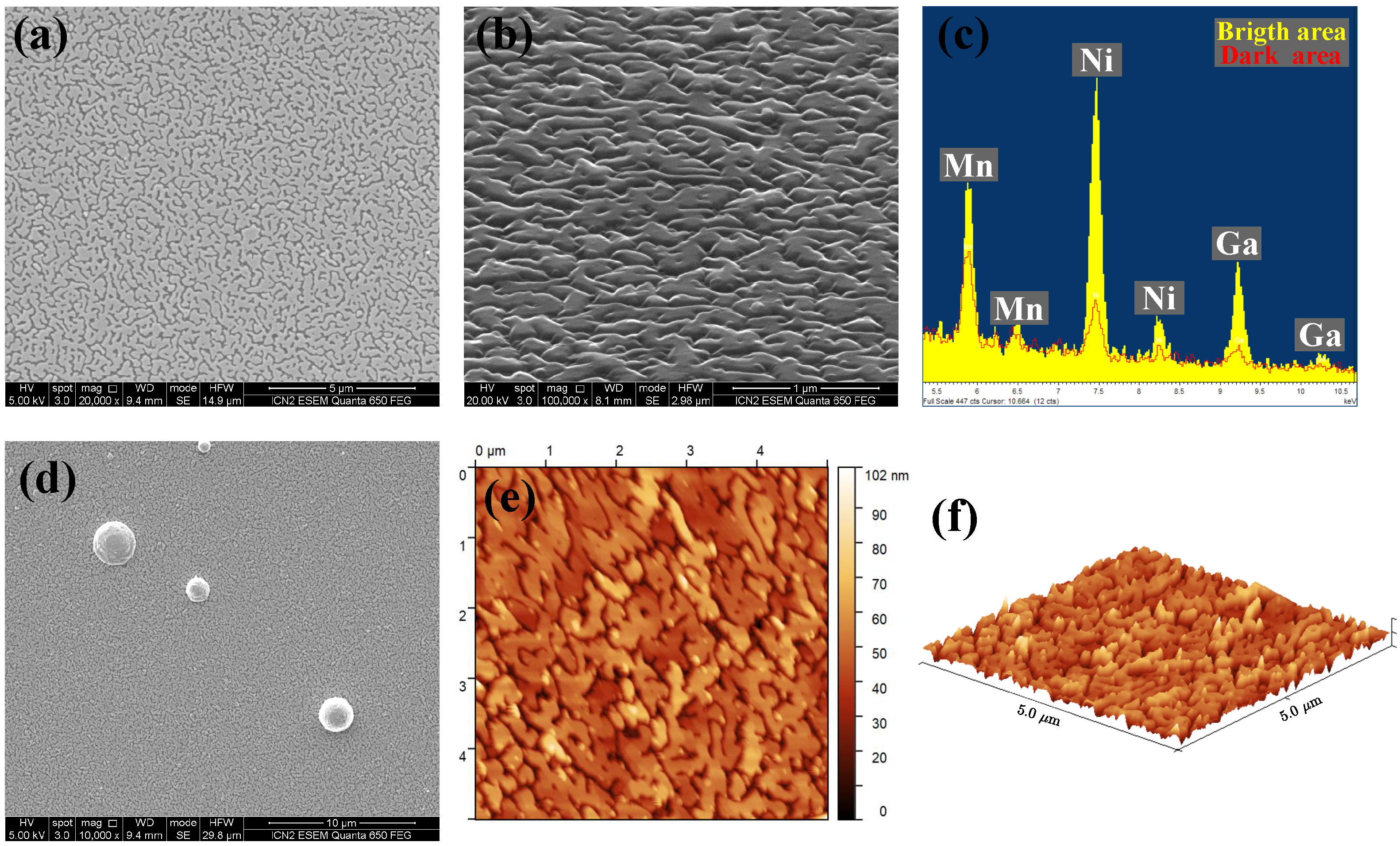
3.1. Film Growth Characteristics

This section discusses the surface topography and film growth mechanism, prior to the analysis of the crystal structure and microstructure. Figure 1a presents a high-magnification view of the film surface. Instead of exhibiting a homogeneous and smooth morphology, the film develops as a percolated metallic layer formed through the coalescence of discrete islands. A tilted-view SEM image is shown in Figure 1b, highlighting the pronounced surface roughness of the sample. A punctual Energy-dispersive X-ray spectroscopy (EDS) analysis was performed on both the bright and dark regions of the surface, as seen in Figure 1c. The analysis revealed a notable decrease in Ni and Ga content in the darker regions between the islands. In contrast, Mn content was reduced to approximately half and became the dominant element in these areas. Considering the high reactivity of Mn with oxygen, the formation of MnO in the valley regions between islands is a plausible hypothesis. An accurate compositional quantification using EDS-SEM was not possible due to the high signal contribution from the substrate. Figure 1d shows an SEM image indicating the presence of spherical droplets on the film surface. Compositional analysis by EDS-SEM identified these droplets as Ni55Mn18Ga27. The droplets’ appearance is due to the ejection of liquid metal caused by partial melting of the target surface during ablation by PLD [25]. Topographical analysis was further performed using AFM, as shown in Figure 1e,f. From Figure 1e, the root mean square (RMS) roughness was calculated to be 12 nm. This value includes contributions from the valleys between islands. When only the islands are considered, the RMS roughness decreases to approximately 7 nm. Figure 1f confirms that the film does not exhibit uniform growth, consistent with the tilted SEM image in Figure 1b. Sharp surface features with heights exceeding 80 nm are visible, while the average island height within the scanned area is approximately 50 nm. The island growth is commonly observed during the growth of dissimilar materials by PLD [26]. For instance, in the growth of a metal film on an insulating substrate, the topography is characterised by evolving from separate islands with the same orientation, to elongated islands that will coalesce with each other to form a percolated metal film, which will eventually fill its hollow spaces. This growth mechanism is known as the Volmer–Weber type.

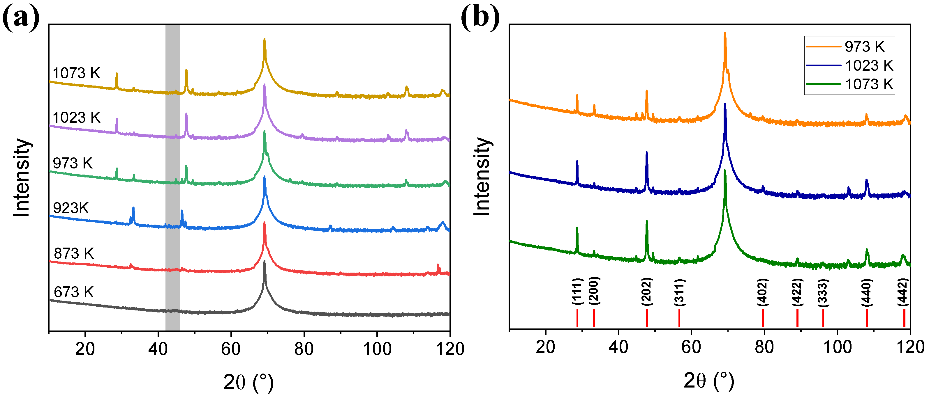
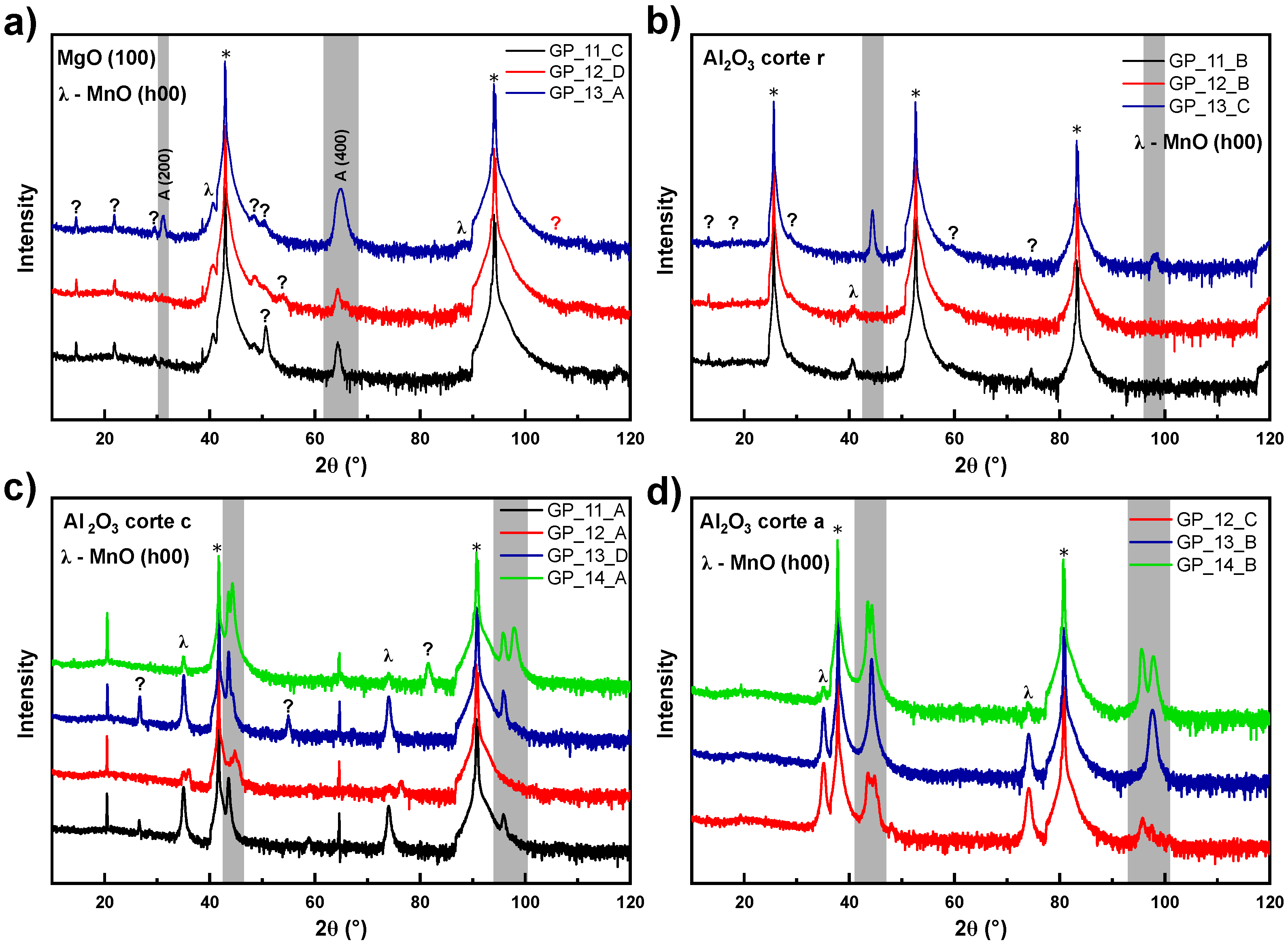
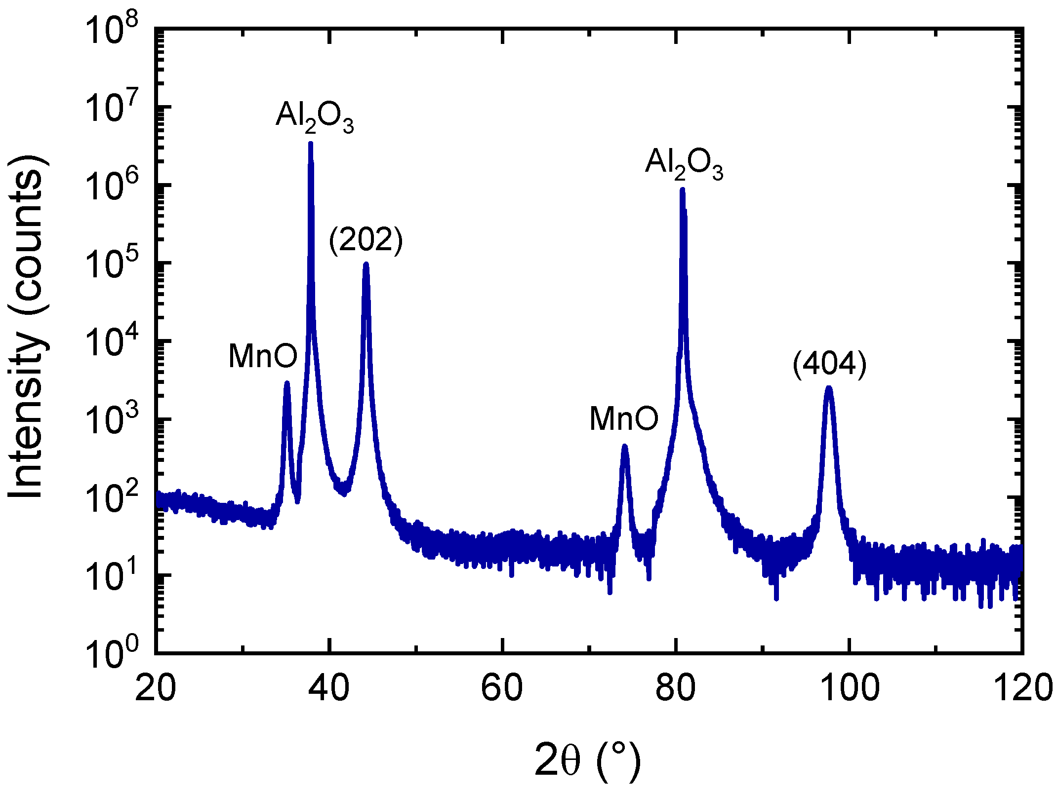
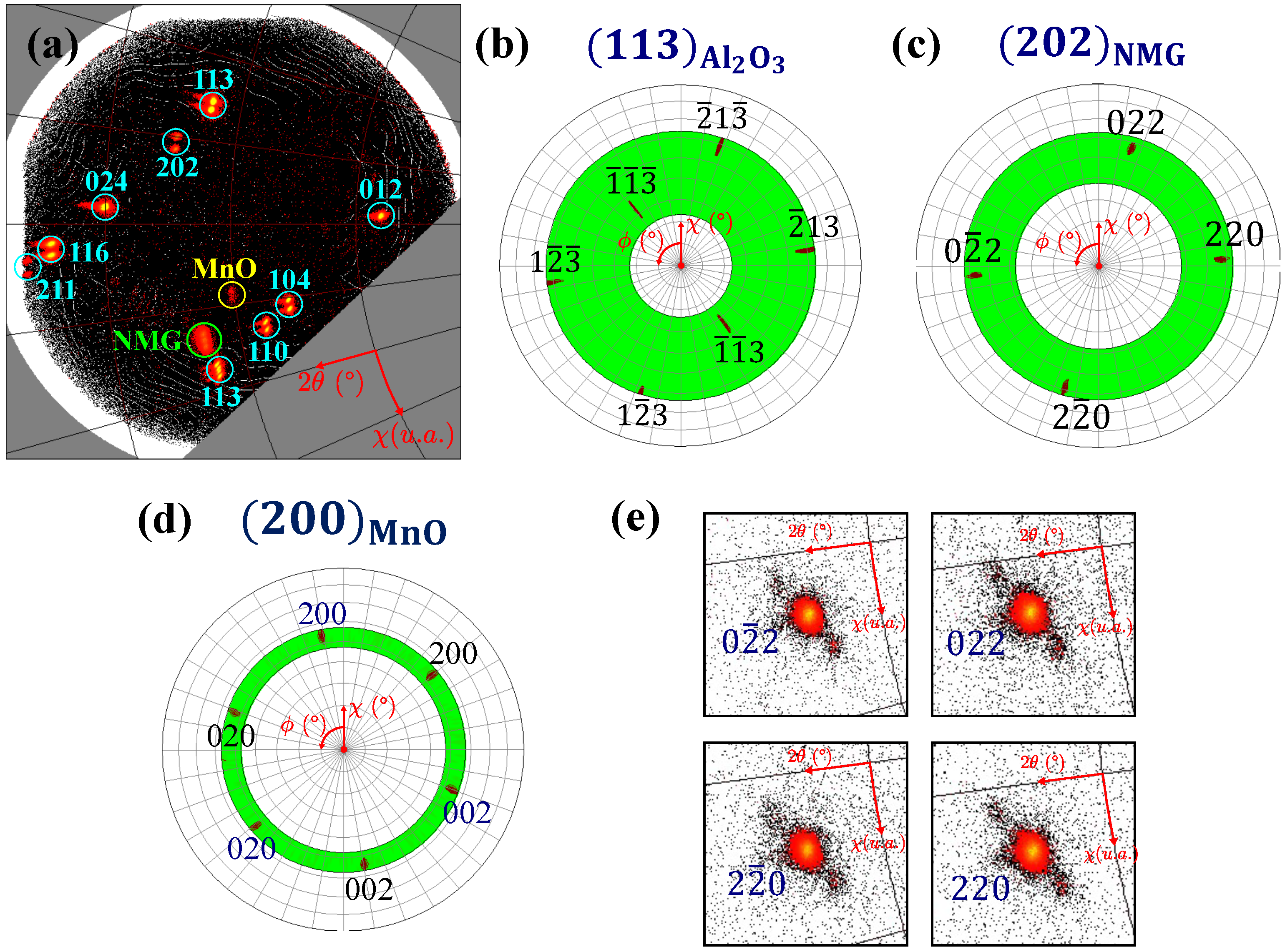
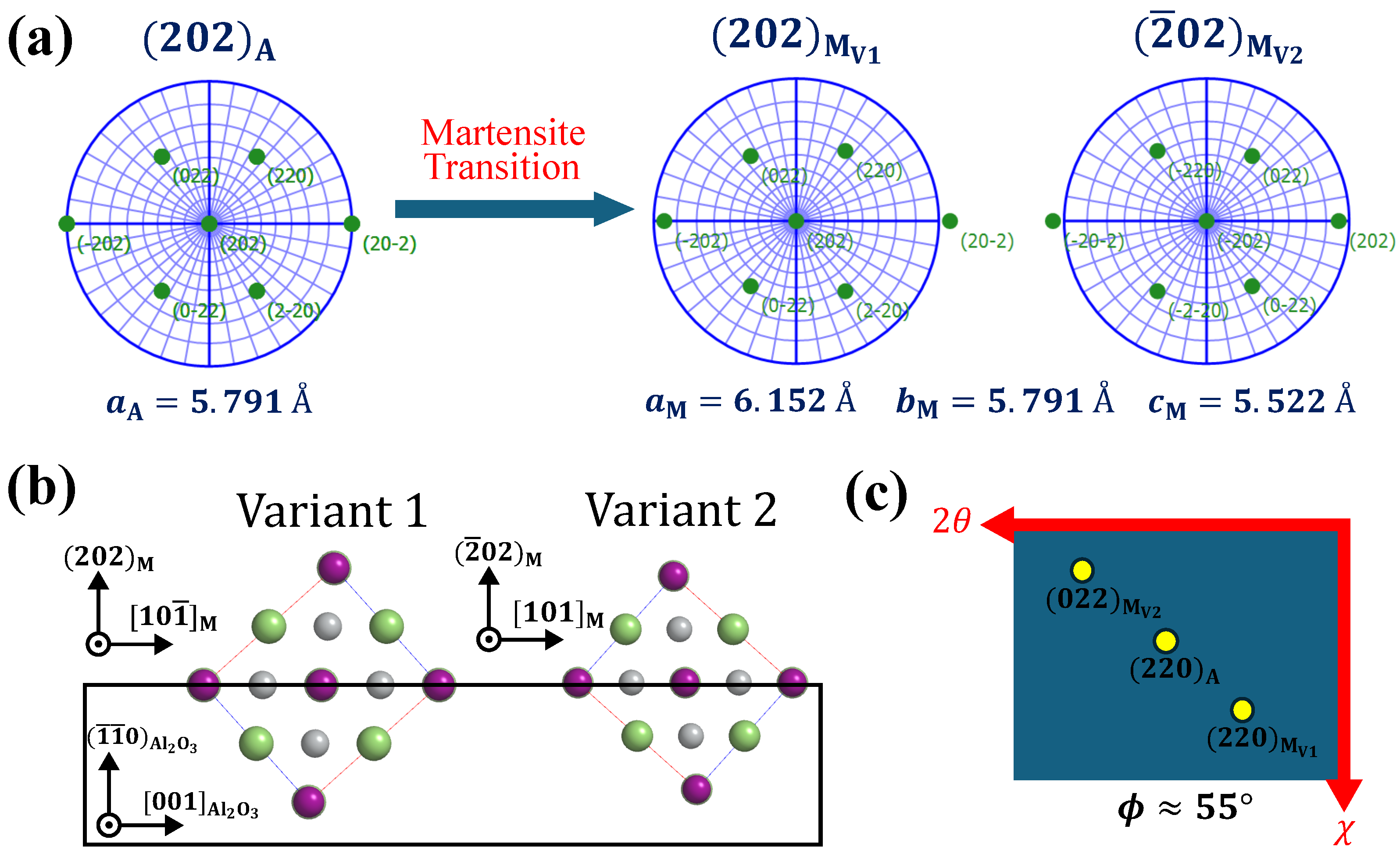
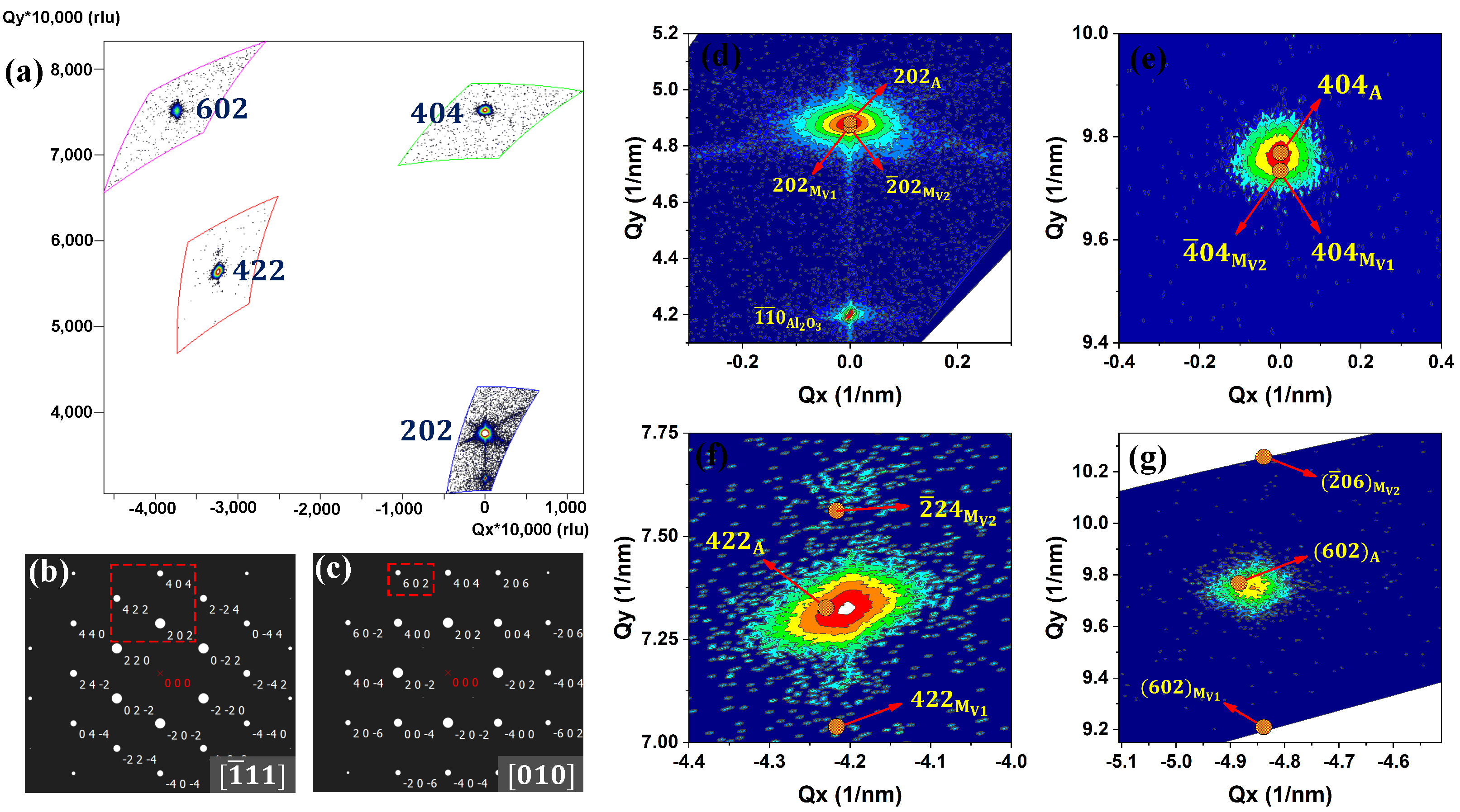
3.2. Determination of Crystalline Structure by X-Ray Diffraction

In this section, the crystal structure of the sample is investigated using various XRD techniques, including symmetrical ω 2 θ scans, pole figures, and reciprocal space maps. Figure 2 displays the XRD pattern obtained from symmetrical ω 2 θ scans in the range of 20–120°. In this pattern, two intense peaks are attributed to the first- and second-order 110 reflections from the a-cut Al2O3 substrate (ICSD collection code 10425). Hereafter, the three-index convention is employed to describe reflections and planes for Al2O3. Four reflections originating from the film are observed. Two of these correspond to the first- and second-order 202 reflections from the NMG phase. Based solely on the symmetrical scan, it is challenging to unambiguously identify the phase and index of the NMG reflections, as the main reflections of the austenite and martensite phases occur in close proximity, within the range of 42–45°. Moreover, these reflections may exhibit shifts relative to their bulk positions due to compositional variations and strain induced by the substrate. Consequently, pole figure and reciprocal space mapping measurements are essential to complement the symmetrical scan and provide reliable phase identification. At this stage, the structure was indexed with respect to the austenitic unit cell (ICSD collection code 190385). Based on the reflections observed in the symmetrical scan, a cubic lattice parameter of a = 5.791 ( 3 ) Å was determined. Additionally, a secondary phase corresponding to cubic MnO, with a lattice parameter of a = 4.423 ( 1 ) Å, was identified in the sample (ICSD collection code 29326). The appearance of just two peaks, corresponding to planes ( 111 ) and ( 222 ) of MnO, indicates that MnO grows highly textured in the out-of-plane direction.
The only presence of h 0 h reflections from the NMG phase indicates a highly textured growth in the out-of-plane direction. To determine the in-plane preferred orientation, and the relationship with the substrate, pole figures of different ( h k l ) planes were measured. The use of a wide-angle GADDS detector allows a fast collection of 2 θ χ maps for different ϕ values. The map in Figure 3a corresponds to an integrated 2 θ χ map over all ϕ angles and reveals several asymmetric reflections from both the film and the substrate. The substrate reflections are labelled in cyan in the map. In the integrated map, it is possible to observe that some peaks from the substrate show multiple components at slightly different χ values. This phenomenon can be attributed to slight tilts of equivalent reflections during the precession in ϕ angle, introduced by imperfect out-of-plane alignment of the sample. To obtain the pole figures of the individual reflections, a narrow 2 θ sector is selected and the corresponding 2 θ χ maps are integrated over the full range of ϕ angles. Figure 3b displays the pole figure of the 113 reflection from the Al2O3 substrate. The green-coloured region denotes the angular range analysed, which contains six well-defined spots corresponding to equivalent crystallographic planes of ( 113 ) , as expected from a Al2O3 single crystal. Figure 3c shows the pole figure of the 202 reflection from the film. The appearance of four distinct spots indicates a pronounced in-plane preferential orientation of the film. For the MnO secondary phase, a pole figure of the 200 reflection was measured, revealing that MnO grows with two in-plane orientations, rotated by 60 with respect to one another; see in Figure 3d. A more detailed examination of each NMG phase reflection observed in Figure 3c reveals the presence of two low-intensity satellite reflections; see Figure 3e. These low intensities of the satellites are indicative of an incipient martensitic phase transition; this will be further discussed in the subsequent section. The results obtained from the symmetrical scan and the pole figure analysis confirm the epitaxial growth of the NMG film on the Al2O3 substrate, with the crystallographic relationship ( 202 ) [ 1 ¯ 01 ] N M G / / ( 1 ¯ 1 ¯ 0 ) [ 001 ] A l 2 O 3 between the film and the substrate.
Considering the reported martensite polytypes, the crystal structure can be tetragonal, for the NM or 5M phases, or monoclinic with a γ close to 90°, for the 7M phase [10]. For practical purposes, the resulting phase can be simulated with an orthorhombic unit cell. The simulations were performed with the open-source software ReciPro [27]. During the transition, the lattice parameter b M of the martensite phase approaches that of the austenite phase a A , while the lattice parameter a M lengthens and c M shrinks with respect to the value of a A [19]. In order to explain the appearance of the satellites in Figure 3e, the chosen lattice parameters were a M = 6.152 Å, b M = 5.791 Å and c M = 5.522 Å. The value of b M was chosen equal to the value calculated from out-of-plane reflection of Figure 2, while a M and c M were calculated from the ratio between the lattice parameters, a 7 M / b 7 M , and c 7 M / b 7 M , given by Brown for a 7M martensite [10]. Due to the reduction in symmetry of the unit cell, the equivalent plane family { 220 } in the austenite phase splits into three equivalent plane subfamilies { 220 } , { 202 } , and { 022 } for the martensite phase. To visualise the symmetry reduction in the pole figure, a pole figure for the { 220 } plane family of austenite phase was simulated, as seen in Figure 4a; for the simulation, a single crystal with the ( 202 ) plane oriented in the out-of-plane direction was considered. After the transition, considering that the resulting martensite phase, which was named variant 1 ( M V 1 ), is oriented with the ( 202 ) plane in the out-of-plane direction, it can be observed that the poles corresponding to the { 220 } and { 022 } family of planes are reoriented, altering their 2 θ and χ value. However, to reproduce the three spots observed in Figure 3e, it is necessary to consider another martensitic variant (variant 2, M V 2 ); see Figure 4b. These variants will grow with their own crystallographic relationships with respect to the substrate, indicated in Figure 4b. Considering this, a pole figure measurement of the sample should observe both structures, which are added to the pole figure of the austenite phase and should produce a 2 θ χ map, as observed in Figure 4c, for a fixed ϕ angle. The fact that Figure 3e shows the formation of such triplets indicates that there is an incipient martensite phase coexisting with a majority austenite phase.
In the martensite phase, the different polytypes (7M or 5M martensite) produce a characteristic pattern in the reciprocal space with the appearance of satellite peaks between two main reflections, which are useful to identify the phases. For example, pure 7M (or 5M) martensite shows six (or four) weak peaks, between intense main peaks along the [ 010 ] 7 M direction (or [ 001 ] 5 M direction) [11,12]. For this reason, in this sample, an exploration of the reciprocal space was performed with reciprocal space mappings (RSMs). Figure 5a shows a combination of RSMs around symmetric 202, 404 reflections and asymmetric 422, 602 reflections. The reflections 202, 404, and 422 were measured at the same azimuthal ϕ -angle, corresponding to the reciprocal space cut shown in Figure 5b. On the other hand, the reflection 602 was measured at a different azimuthal ϕ -angle, which corresponds to the reciprocal space cut shown in Figure 5c. Figure 5b,c are simulated reciprocal space patterns (the simulations were performed with the open-source software ReciPro [27]) from the austenite phase, considering the ( 202 ) out-of-plane orientation. In the Q x = 0 coordinate of the map, it is possible to observe the 202 and 404 symmetrical reflections as well as the out-of-plane 1 ¯ 1 ¯ 0 reflection from the Al2O3 substrate. In addition, the 202 reflection shows the appearance of obliquus streaks, which seem to connect towards the lower Q y region from symmetric 202 to asymmetric 220 and 0 2 ¯ 2 reflections. In the RSM of 440, the streaking was not observed, probably because of the weak intensity of these lines. In Figure 5d, the measured reflection 202 was compared with its respective reflections taken from austenite phase and martensite variants ( M V 1 and M V 2 ) proposed in Figure 4b. Explanatory information about the simulation of RSM of martensite variants is shown in Appendix B. The comparison shows that reflections from martensite variants, 202 M V 1 and 2 ¯ 02 M V 2 , slightly shrink in respect to austenite reflection 202 A . This effect is best observed in the second-order reflection 404; see Figure 5e. In addition, the symmetric reflections 202 M V 1 and 2 ¯ 02 M V 2 (and their second-order reflections) do not show appreciable differences. This is because M V 1 and M V 2 share equivalent planes, oriented in the out-of-plane direction; see Figure 4. For the case of non-symmetrical reflections, it is expected that they will be different because the orientation of the planes is not equivalent. Figure 5f shows the comparison between the measured reflection 422 with respect to the reflection obtained from the austenite and martensite phases modelled in Figure 4. In this comparison, a large splitting was observed between the reflections, specially for 422 M V 1 and 2 ¯ 24 M V 2 . In this case, the measured reflection is closer to the austenite 422 A reflection than the other reflections. In addition, it was observed that the high intense spot from reflection 422 is accompanied with two weak contributions, above and below the intense peak. These two contributions appear to correspond to martensite variants, which can indicate an incipient transformation from austenite to martensite phase. This result supports the observations performed by pole figure; see Figure 3e. The asymmetric 602 reflection was compared with reflections from austenite and martensite modelled structures in Figure 5g. From the comparison, it is observed that the measured reflection is again closer to austenite reflection than any of the possible martensite reflections. In this case, no trace of the martensite reflections was observed, probably because they are weak. These results support the previous assumption that the studied sample has a slightly distorted austenite crystalline structure.
From the RSM measurements the interplanar distances for each reflection were obtained with high precision. Therefore, it was possible to determine the distortions in the film’s structure, with respect to a perfect austenite. For that, an orthorhombic unit cell model was used, where the lattice parameters were varied in order to fit with the interplanar distances calculated from each reflection. The best match was obtained with lattice parameters a = 5.8085 ( 1 ) Å, b = 5.804 ( 1 ) Å, and c = 5.7786 ( 3 ) Å, which show a slight lattice distortion in the c axis of about 0.5% respect to the others. Typically, in the martensite phase, the axes of the austenite phase suffer a distortion according the polytype of the martensite phase. For example, Brown et al. [10] show that for the 5M martensite, the cell is a body-centred tetragonal with a = 5.90 Å, c = 5.54 Å ( c / a 0.94 ). In the case of 7M martensite, the cell is a body-centred monoclinic with a = 6.14 Å, b = 5.78 Å, c = 5.51 Å, γ = 90 . 58 ( c / a 0.89 ). The non-modulated martensite cell is a body-centred tetragonal with a = 5.52 Å and c = 6.44 Å ( c / a 1.17 ). For the case of modulated martensite, the ratio c / a is less than one. In our film, the a and b axes are almost similar, and only the c axis shrinks. However, the shrinkages with respect to the other axis are c / a 0.995 and c / a 0.996 . The distortion is ten times smaller than the reported martensite, so it does not correspond to a proper martensite phase but the distortions could be related to strain imposed by the substrate constraint. This result indicates that the main crystal structure of the sample is a slightly distorted cubic austenite phase.

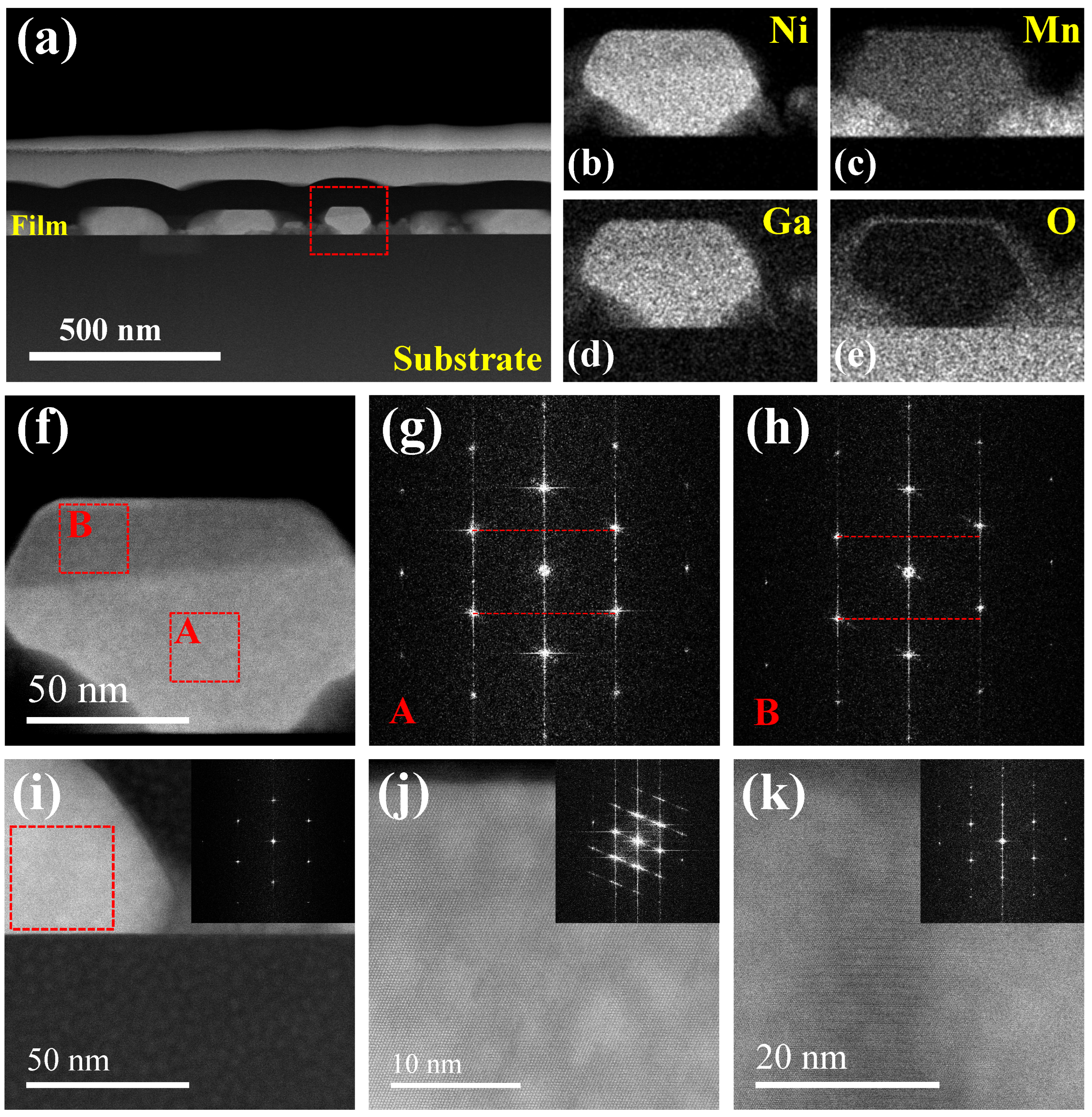
3.3. Microstructure Observed by Transmission Electron Microscopy

Following the established relationships determined by X-ray measurements, a specific cross section was chosen to prepare a lamella for TEM analysis, such that the zone axis of the film was [ 1 ¯ 11 ] . This was chosen because this is the characteristic cut where the structure modulations are expected to show satellites reflections. In Figure 6a, a cross-section view of the film at low magnification is observed. This image shows a non-homogeneous film, as it was also observed in SEM images, with an approximate thickness of 70 nm. A zoom was performed in one island, and elemental mapping were carried out by EDS. The EDS mapping from K α lines of Ni, Mn, Ga, and O are shown in Figure 6b–e. The calculated chemical composition of the film was Ni56Mn18Ga26, very close to the chemical composition of the droplets observed by SEM. The high concentration of Mn and O between the islands is proof that MnO is formed in the gaps between the connected islands, as was suggested by SEM. The oxygen distribution in mapping Figure 6e indicates that the island is almost free of oxygen contamination, even when the film was not protected. From Figure 6f, which corresponds to a magnified image of the analysed island in HAADF-STEM mode, comparing the contrast, it is possible to observe that the island shows two parts: one brighter part closer to the substrate (A), and a darker part in the upper part of the island (B), probably corresponding to two separate NMG phases. These two phases were analysed by EDS separately and both have the same chemical composition. Therefore, their difference is basically in their crystal structure, as it is shown in the Fast Fourier Transform (FFT) from each phase; see Figure 6g,h, for A and B regions, respectively. In this case, it is possible to see that the A phase closer to the substrate does not suffer large distortions, showing an almost perfect hexagonal pattern characteristic of the cubic structure with [ 1 ¯ 11 ] zone axis, as compared to the upper phase B. The distortions can be compared from the FFT images marked with red lines for reference. Using the fitting respect to an orthorhombic unit cell, it is possible to quantify the distortion by the ratio between the a (that elongates) and c (that shrinks) axes. Therefore, from Figure 6g, the ratio is c / a 0.986 and from Figure 6h, the ratio is c / a 0.894 . The large distortions can be related to an incipient martensitic phase transition, which typically occurs close to room temperature. The fact that the regions close to the substrate are those showing slight distortions seems to indicate that the substrate imposes a strong constrain, which strongly prevents the martensite phase transition to occur. A close inspection in different regions across the lateral distance of the film shows a wide range of distortions of the crystal structure, as well as the coexistence of the austenite phase and small regions in their martensite phase. For instance, in Figure 6i, it is possible to observe another region close to the substrate, different to that shown in Figure 6f, with a negligible distortion with respect the austenite phase ( c / a 0.990 ). The inset of Figure 6i shows the diffraction pattern obtained by the FFT of the region in the red box of the same image. In contrast, in Figure 6j, a region close to the top surface of the film shows the presence of obliquus lines alternating bright and dark contrast in atomic scale resolution. The corresponding FFT image presents diagonal streaks between main reflections, which are indicative of incipient modulations in the [ 110 ] direction ( c / a 0.753 ). In another part of the sample, as depicted in Figure 6k, it is possible to observe the appearance of the formation of a clear modulation along the vertical direction, corresponding to the 5M martensite phase. The corresponding FFT indicates a superstructure with four additional satellites between the main reflections along the vertical direction. The deformation calculated from its main reflection was c / a 0.937 , a value close to that reported for 5M martensite [10].
Another remarkable observation derived from the HR-STEM analysis is that in all the regions analysed, i.e.,: islands of about 100 nm lateral size, the transformed upper regions seem to proceed in the same crystallographic direction. According to the model presented in Figure 4, these distortions correspond to the formation of martensite M V 1 . Note, for instance, that both FFTs in Figure 6h,j show the same type of pattern distortion. We did not observe any region with the coexistence of M V 1 and M V 2 . This is an indication that distortions take place monolithically in every island. However, the XRD analysis indicated the presence of M V 1 and M V 2 , streaks in the 202 reciprocal space map in Figure 5a. Therefore, it is expected that other local regions in the film will transform in individual crystallographic orientations.

4. Discussion

Most of the observed islands exhibit an incipient transformation towards a martensite-distorted phase, with varying degrees of distortion. In contrast, regions near the interface with the substrate remain nearly undistorted in the austenite phase. As previously mentioned, this suggests that the elastic constraint imposed by the Al2O3 substrate inhibits the phase transformation. Additionally, the epitaxial constraint from the substrate is expected to affect domain boundary motion, which is crucial for achieving a large MFIS and a fast response suitable for applications. Although characterising the MFIS of these films was not within the scope of this study, it is anticipated that significant MFIS values would not be observed within this thickness range. A substantial increase in film thickness or the use of lithographic techniques to define suspended film sections would be required to mitigate substrate constraints. Although these films may not be directly applicable to practical uses, the high crystalline quality of the Ni-Mn-Ga thin films provides a valuable platform for further fundamental crystallographic studies and their correlation with magnetic and electronic properties. Furthermore, with advancements in techniques for fabricating free-standing membranes, it is now possible to detach the epitaxial film from the substrate using sacrificial layers and investigate its MFIS properties without substrate-induced constraints.

5. Conclusions

Epitaxial Ni-Mn-Ga thin films were grown on Al2O3 ( 11 2 ¯ 0 ) single-crystal substrates using the PLD technique. The growth process follows the Volmer–Weber mechanism, which is commonly observed in systems involving dissimilar materials, such as insulators and metals. A comprehensive analysis of the crystal structure was conducted using various XRD techniques. Due to ambiguities in symmetrical scans and pole figure measurements, XRD reciprocal space mapping was performed for different reflections. These analyses revealed that the sample predominantly exhibits an austenite-like phase at room temperature, though indications of an incipient martensitic transition were observed. While the martensite phase is not fully developed, pole figure and reciprocal space measurements show the presence of localised martensitic regions. A microstructural study using HR-STEM further confirmed the presence of regions with a 5M martensite phase. Additionally, structural distortions were observed, appearing more pronounced in areas further from the substrate, while regions near the substrate remained almost undistorted. This finding supports the hypothesis that the substrate imposes a constraint on the film, stabilising the austenite phase and inhibiting the phase transition. Overall, this study demonstrates that PLD is an effective technique for obtaining epitaxial Ni-Mn-Ga thin films with high crystalline quality. Moreover, achieving film thicknesses well above 100 nm is necessary to reduce the substrate constraints and enable the exploration of magnetic-field-induced strain.

Author Contributions

Conceptualisation, M.G.P.-C. and J.Q.-M.; methodology, J.M.C.-R., J.P.-P. and J.S.; software, M.G.P.-C. and J.S.; validation, J.M.C.-R., J.S. and J.P.-P.; formal analysis, M.G.P.-C.; investigation, M.G.P.-C.; resources, J.M.C.-R., J.P.-P. and J.S.; data curation, J.P.-P. and J.S.; writing—original draft preparation, M.G.P.-C.; writing—review and editing, J.Q.-M., C.V.L., V.A.P.-R. and J.S.; visualisation, M.G.P.-C.; supervision, J.Q.-M. and J.S.; project administration, V.A.P.-R.; funding acquisition, V.A.P.-R. All authors have read and agreed to the published version of the manuscript.

Funding

The authors acknowledge PROCIENCIA-CONCYTEC for funding the project under contract code PE501079047-2022. This research was further supported by the Universidad Nacional Mayor de San Marcos (Project numbers: B23131861 and B22139675x). G.P. acknowledges funding from the European Union’s Horizon 2020 research and innovation program under the Marie Sklodowska-Curie grant agreement No. 101007825 (ULTIMATE-I Project) for a research stay at ICN2. This research was also funded by the European Union’s Horizon 2020 research and innovation programme under grant agreement No. 101007417, having benefitted from the access provided by ICN2 in Bellaterra (Spain) within the framework of the NFFA-Europe Pilot Transnational Access Activity, proposal ID530. ICN2 is supported by the Severo Ochoa program from Spanish MCIN/AEI (Grant No.: CEX2021-001214-S) and is funded by the CERCA Programme.

Institutional Review Board Statement

Not applicable.

Informed Consent Statement

Not applicable.

Data Availability Statement

The research data can be requested from the corresponding author.

Acknowledgments

G.P. acknowledges David Pesquera for the help with AFM measurements, Francisco Belarre for lamella preparation by FIB, Bernat Mundet for the HR-(S)TEM measurements, and Marcos Rosado for the SEM measurements.

Conflicts of Interest

The authors declare no conflicts of interest.

Abbreviations

The following abbreviations are used in this manuscript:
MSMAMagnetic Shape Memory Alloy
PLDPulsed Laser Deposition
NMGNi-Mn-Ga
HR-(S)TEMHigh-Resolution Scanning Transmission Electron Microscopy
SEMScanning Electron Microscopy
XRDX-ray Diffraction
RSMsReciprocal Space Maps

Appendix A. Sample Optimisation

During the optimisation process, samples were grown on Si ( 100 ) , MgO ( 100 ) , Al2O3  ( 11 2 ¯ 0 ) , Al2O3  ( 0001 ) , and Al2O3  ( 01 1 ¯ 2 ) single-crystal substrates. In order to reproduce the works of Hakola [23] and Tello [22], thin films of Ni-Mn-Ga were grown in Si ( 100 ) at different temperatures. The XRD measurements of the samples grown on Si ( 100 ) substrate are shown in Figure A1a. In Figure A1a, the grey box indicates the range where the main reflections from austenite or martensite phase are expected to be. Unfortunately, no NMG main reflections were observed (the intensity axis was plotted in log form to see low intensity peaks). However, other phases were formed, which were expected from the reaction between the films and the substrate. At high temperatures ( T > 950 K), the main phase is NiSi2. In Figure A1b, the identification of the reflections was performed. Other phases were not identified.
Figure A1. (a) XRD pattern comparison of samples grown on silicon at different temperatures. The grey box indicates the region where the main reflection from NMG is expected to be. (b) Phase identification of polycrystalline NiSi2.
Surfaces 08 00035 g0a1
In Figure A2, the XRD pattern of samples grown on MgO ( 100 ) , Al2O3  ( 11 2 ¯ 0 ) , Al2O3  ( 0001 ) , and Al2O3  ( 01 1 ¯ 2 ) are shown. In all these samples, reflections from the NMG were observed, but also, non-identified phases were observed. In MgO (100) substrates, a growth of austenite phase was identified. However, this sample shows other non-identified phases. On the other hand, the Al2O3 single-crystal substrate appears to be more suitable for the growth of NMG in different phases. However, the problem of the appearance of a non-NMG phase is present. The Al2O3  ( 01 1 ¯ 2 ) single-crystal substrate appears to be more suitable for the growth of NMG because of the low lattice mismatch [18,19] and the optimised sample of this set of samples was chosen to analyse.
Figure A2. XRD patterns measured from samples growth on single-crystal substrates of (a) MgO ( 100 ) , (b) Al2O3  ( 01 1 ¯ 2 ) , (c) Al2O3  ( 0001 ) , and (d) Al2O3  ( 11 2 ¯ 0 ) . In the figures, “*” indicate the substrate peaks, “?” indicate the unkwonw peaks and “ λ ” correspond to MnO peaks.
Surfaces 08 00035 g0a2

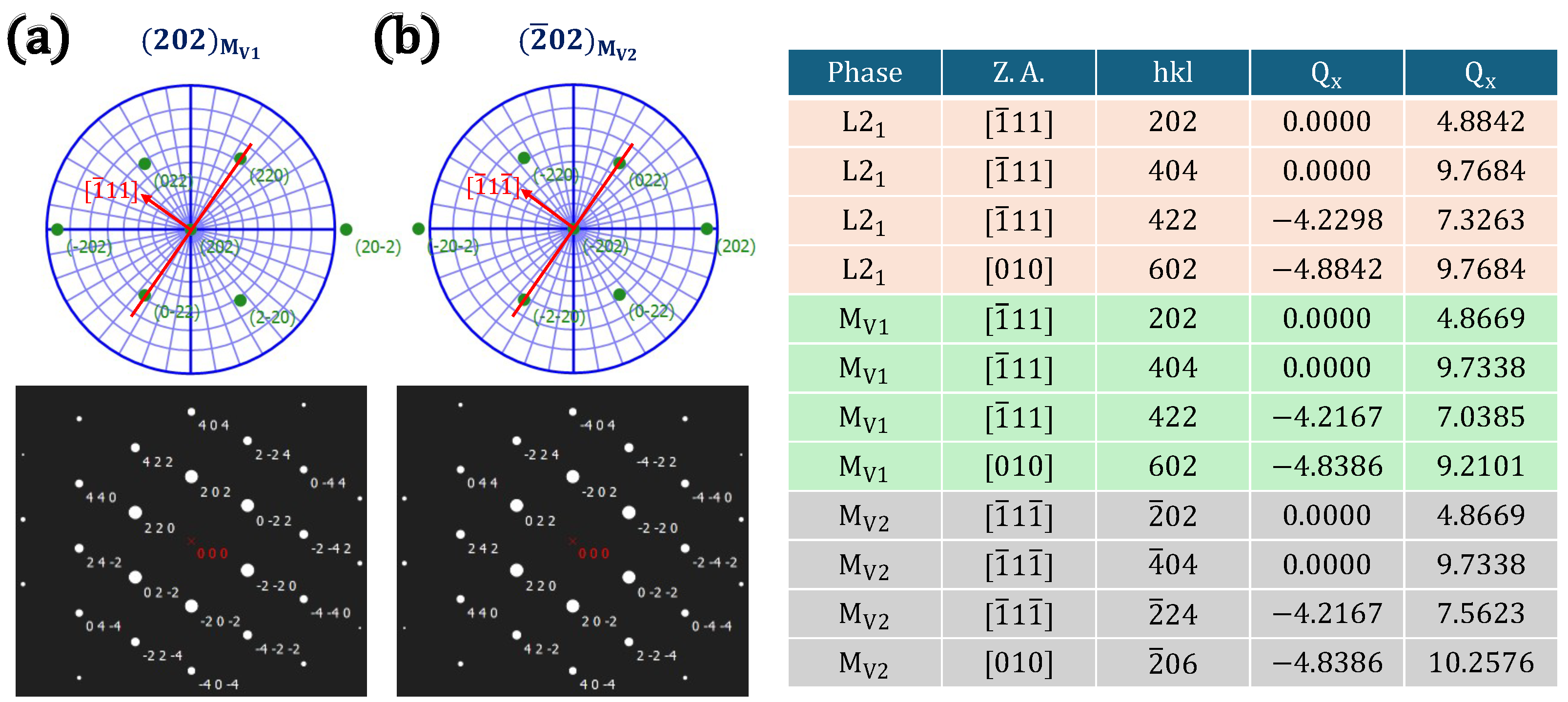
Appendix B. RSM for Martensite Variants

From the structure models proposed in the Figure 4 for austenite and martensite phases (considering each variant), RSM simulations were performed; see Figure A3. The simulated RSMs were taken from zone [ 1 ¯ 11 ] for M V 1 and [ 1 ¯ 1 1 ¯ ] for M V 2 . In Figure A3, the pole figure of each variant is shown, indicating where the RSM cut was performed, and the direction of the zone axis. In addition, a table with the x y reciprocal space coordinates for each reflection used in the comparison in Figure 5d–g is presented. All the simulations were performed using the software ReciPro [27].
Figure A3. Simulated reciprocal space pattern of martensite variants M V 1 and M V 2 presented in Figure 4. The reciprocal map corresponds to zone [ 1 ¯ 11 ] for (a) and [ 1 ¯ 1 1 ¯ ] for (b). Table with the x y reciprocal space coordinates (in nm−1 units).
Surfaces 08 00035 g0a3

References

  1. Yu, G.H.; Xu, Y.L.; Liu, Z.H.; Qiu, H.M.; Zhu, Z.Y.; Huang, X.P.; Pan, L.Q. Recent progress in Heusler-type magnetic shape memory alloys. Rare Met. 2015, 34, 527–539. [Google Scholar] [CrossRef]
  2. Karaca, H.; Karaman, I.; Basaran, B.; Lagoudas, D.; Chumlyakov, Y.; Maier, H. On the stress-assisted magnetic-field-induced phase transformation in Ni2MnGa ferromagnetic shape memory alloys. Acta Mater. 2007, 55, 4253–4269. [Google Scholar] [CrossRef]
  3. Ullakko, K.; Huang, J.K.; Kantner, C.; O’Handley, R.C.; Kokorin, V.V. Large magnetic-field-induced strains in Ni2MnGa single crystals. Appl. Phys. Lett. 1996, 69, 1966–1968. [Google Scholar] [CrossRef]
  4. Kainuma, R.; Imano, Y.; Ito, W.; Sutou, Y.; Morito, H.; Okamoto, S.; Kitakami, O.; Oikawa, K.; Fujita, A.; Kanomata, T.; et al. Magnetic-field-induced shape recovery by reverse phase transformation. Nature 2006, 439, 957–960. [Google Scholar] [CrossRef]
  5. Ranzieri, P.; Campanini, M.; Fabbrici, S.; Nasi, L.; Casoli, F.; Cabassi, R.; Buffagni, E.; Grillo, V.; Magén, C.; Celegato, F.; et al. Achieving Giant Magnetically Induced Reorientation of Martensitic Variants in Magnetic Shape-Memory Ni–Mn–Ga Films by Microstructure Engineering. Adv. Mater. 2015, 27, 4760–4766. [Google Scholar] [CrossRef]
  6. Murray, S.J.; Marioni, M.A.; Kukla, A.M.; Robinson, J.; O’Handley, R.C.; Allen, S.M. Large field induced strain in single crystalline Ni–Mn–Ga ferromagnetic shape memory alloy. J. Appl. Phys. 2000, 87, 5774–5776. [Google Scholar] [CrossRef]
  7. Sozinov, A.; Likhachev, A.A.; Lanska, N.; Ullakko, K. Giant magnetic-field-induced strain in NiMnGa seven-layered martensitic phase. Appl. Phys. Lett. 2002, 80, 1746–1748. [Google Scholar] [CrossRef]
  8. Ullakko, K.; Ezer, Y.; Sozinov, A.; Kimmel, G.; Yakovenko, P.; Lindroos, V. Magnetic-field-induced strains in polycrystalline Ni-Mn-Ga at room temperature. Scr. Mater. 2001, 44, 475–480. [Google Scholar] [CrossRef]
  9. Chmielus, M.; Zhang, X.X.; Witherspoon, C.; Dunand, D.C.; Müllner, P. Giant magnetic-field-induced strains in polycrystalline Ni–Mn–Ga foams. Nat. Mater. 2009, 8, 863–866. [Google Scholar] [CrossRef]
  10. Brown, P.J.; Crangle, J.; Kanomata, T.; Matsumoto, M.; Neumann, K.U.; Ouladdiaf, B.; Ziebeck, K.R.A. The crystal structure and phase transitions of the magnetic shape memory compound Ni2MnGa. J. Phys. Condens. Matter 2002, 14, 10159–10171. [Google Scholar] [CrossRef]
  11. Cong, D.Y.; Wang, Y.D.; Zetterström, P.; Peng, R.L.; Delaplane, R.; Zhao, X.; Zuo, L. Crystal structures and textures of hot forged Ni48Mn30Ga22alloy investigated by neutron diffraction technique. Mater. Sci. Technol. 2005, 21, 1412–1416. [Google Scholar] [CrossRef]
  12. Glavatskyy, I.; Glavatska, N.; Urubkov, I.; Hoffman, J.U.; Bourdarot, F. Crystal and magnetic structure temperature evolution in Ni–Mn–Ga magnetic shape memory martensite. Mater. Sci. Eng. A 2008, 481–482, 298–301. [Google Scholar] [CrossRef]
  13. Sozinov, A.; Likhachev, A.A.; Lanska, N.; Soderberg, O.; Ullakko, K.; Lindroos, V.K. Effect of crystal structure on magnetic-field-induced strain in Ni-Mn-Ga. In Smart Structures and Materials 2003: Active Materials: Behavior and Mechanics; Lagoudas, D.C., Ed.; SPIE: Bellingham, WA, USA, 2003; Volume 5053, p. 586. [Google Scholar] [CrossRef]
  14. Gruner, M.E.; Niemann, R.; Entel, P.; Pentcheva, R.; Rößler, U.K.; Nielsch, K.; Fähler, S. Modulations in martensitic Heusler alloys originate from nanotwin ordering. Sci. Rep. 2018, 8, 8489. [Google Scholar] [CrossRef]
  15. Wei, Z.Y.; Liu, E.K.; Li, Y.; Han, X.L.; Du, Z.W.; Luo, H.Z.; Liu, G.D.; Xi, X.K.; Zhang, H.W.; Wang, W.H.; et al. Magnetostructural martensitic transformations with large volume changes and magneto-strains in all-d-metal Heusler alloys. Appl. Phys. Lett. 2016, 109, 071904. [Google Scholar] [CrossRef]
  16. Dunand, D.C.; Müllner, P. Size Effects on Magnetic Actuation in Ni-Mn-Ga Shape-Memory Alloys. Adv. Mater. 2010, 23, 216–232. [Google Scholar] [CrossRef]
  17. Ranzieri, P.; Fabbrici, S.; Nasi, L.; Righi, L.; Casoli, F.; Chernenko, V.A.; Villa, E.; Albertini, F. Epitaxial Ni–Mn–Ga/MgO(100) thin films ranging in thickness from 10 to 100 nm. Acta Mater. 2013, 61, 263–272. [Google Scholar] [CrossRef]
  18. Sharma, A.; Mohan, S.; Suwas, S. Structural transformations in highly oriented seven modulated martensite Ni–Mn–Ga thin films on an Al2O3 substrate. J. Mater. Res. 2016, 31, 3016–3026. [Google Scholar] [CrossRef]
  19. Sharma, A.; Mohan, S.; Suwas, S. Evidence of adaptive modulation and magnetic field induced reorientation of variants in epitaxially grown Ni-Mn-Ga thin film on Al2O3 (11-20) substrate. Mater. Sci. Eng. B 2019, 242, 6–16. [Google Scholar] [CrossRef]
  20. Yang, B.; Soldatov, I.; Chen, F.; Zhang, Y.; Li, Z.; Yan, H.; Schäfer, R.; Wang, D.; Esling, C.; Zhao, X.; et al. Observation of magnetic domain evolution in constrained epitaxial Ni–Mn–Ga thin films on MgO(0 0 1) substrate. J. Mater. Sci. Technol. 2022, 102, 56–65. [Google Scholar] [CrossRef]
  21. Kar, S.; Ikeda, Y.; Lünser, K.; Woodcock, T.G.; Nielsch, K.; Reith, H.; Maaß, R.; Fähler, S. Growth Twins and Premartensite Microstructure in Epitaxial Ni-Mn-Ga Films. Acta Mater. 2023, 252, 118902. [Google Scholar] [CrossRef]
  22. Tello, P.G.; Castaño, F.J.; O’Handley, R.C.; Allen, S.M.; Esteve, M.; Castaño, F.; Labarta, A.; Batlle, X. Ni–Mn–Ga thin films produced by pulsed laser deposition. J. Appl. Phys. 2002, 91, 8234–8236. [Google Scholar] [CrossRef]
  23. Hakola, A.; Heczko, O.; Jaakkola, A.; Kajava, T.; Ullakko, K. Pulsed laser deposition of NiMnGa thin films on silicon. Appl. Phys. A 2004, 79, 1505–1508. [Google Scholar] [CrossRef]
  24. Zhang, Y.; Hughes, R.; Preston, J.; Botton, G.; Niewczas, M. Texture and Microstructure Studies on Films of Ni-Mn-Ga Produced by R. F. Sputtering and Pulsed Laser Deposition. In State-of-the-Art Research and Application of SMAs Technologies; Trans Tech Publications Ltd.: Bäch, Switzerland, 2008; Volume 59, pp. 11–17. [Google Scholar] [CrossRef]
  25. Yoshitake, T.; Shiraishi, G.; Nagayama, K. Elimination of droplets using a vane velocity filter for pulsed laser ablation of FeSi2. Appl. Surf. Sci. 2002, 197–198, 379–383. [Google Scholar] [CrossRef]
  26. Aziz, M.J. Film growth mechanisms in pulsed laser deposition. Appl. Phys. A 2008, 93, 579–587. [Google Scholar] [CrossRef]
  27. Seto, Y.; Ohtsuka, M. ReciPro: Free and open-source multipurpose crystallographic software integrating a crystal model database and viewer, diffraction and microscopy simulators, and diffraction data analysis tools. J. Appl. Crystallogr. 2022, 55, 397–410. [Google Scholar] [CrossRef]
Figure 1. (a) SEM image of the thin film surface showing a percolating metal film behaviour of the sample. (b) Tilt SEM image showing an irregular topography. (c) EDS spectrum from a punctual mapping between the bright zone and dark zone of the sample. (d) SEM image of the top-view of the sample showing the presence of droplets. (e) AFM measurement from an area of 5 μ m × 5 μ m. (f) Three-dimensional projection from the AFM measurement showing roughness in the sample.
Surfaces 08 00035 g001
Figure 2. X-ray diffraction pattern from the as-deposited sample. The two high intensity peaks correspond to 202 and 404 reflections from the film. Two reflections from a second phase, identified as MnO, are also observed.
Surfaces 08 00035 g002
Figure 3. The pole figures of the sample show the in-plane preferred orientation, and the relationship between the films and the substrate. Figure (a) shows the integrated map with the high intense reflections observed during the scan. Pole figure of equivalent (b) ( 113 ) A l 2 O 3 , (c) ( 202 ) N M G , and (d) ( 200 ) M n O planes. (e) The 2 θ χ maps for each pole observed in (c) shows that principal reflections are accompanied by two weak satellites.
Surfaces 08 00035 g003
Figure 4. (a) Schematic representation of the effect of the martensitic phase transition on the pole figure. (b) A model is presented considering an orthorhombic unit cell of a sample exhibiting two martensitic variants. (c) Schematic 2 θ χ map, taken for a ϕ = 55 , considering the two variant contributions.
Surfaces 08 00035 g004
Figure 5. (a) Reciprocal space mapping measurements taken from 202, 404, 422, and 602 reflections. Figure (b,c) show simulated reciprocal space pattern from austenite phase. From Figure (dg), the reciprocal space maps from each reflection observed in Figure (a) are compared with reflections from the martensite variant presented in Figure 4 and the austenite phase.
Surfaces 08 00035 g005
Figure 6. (a) HR-(S)TEM image of the thin film cross section. (be) EDS elemental mapping from the K α lines of Ni, Mn, Ga, and O. (f) HR-(S)TEM image of one island in the film. The FFT of zones A and B, indicated in (f), are shown in (g,h), respectively. High-magnification HR-STEM image from zones close to (i) the substrate and (j) the top of the film. (k) Observation of a region in its 5M martensite phase.
Surfaces 08 00035 g006
Disclaimer/Publisher’s Note: The statements, opinions and data contained in all publications are solely those of the individual author(s) and contributor(s) and not of MDPI and/or the editor(s). MDPI and/or the editor(s) disclaim responsibility for any injury to people or property resulting from any ideas, methods, instructions or products referred to in the content.

