Synthesis of MoS2 Thin Film by Ionized Jet Deposition: Role of Substrate and Working Parameters

 ,
,  ,
,  , and
, and 
Abstract
1. Introduction
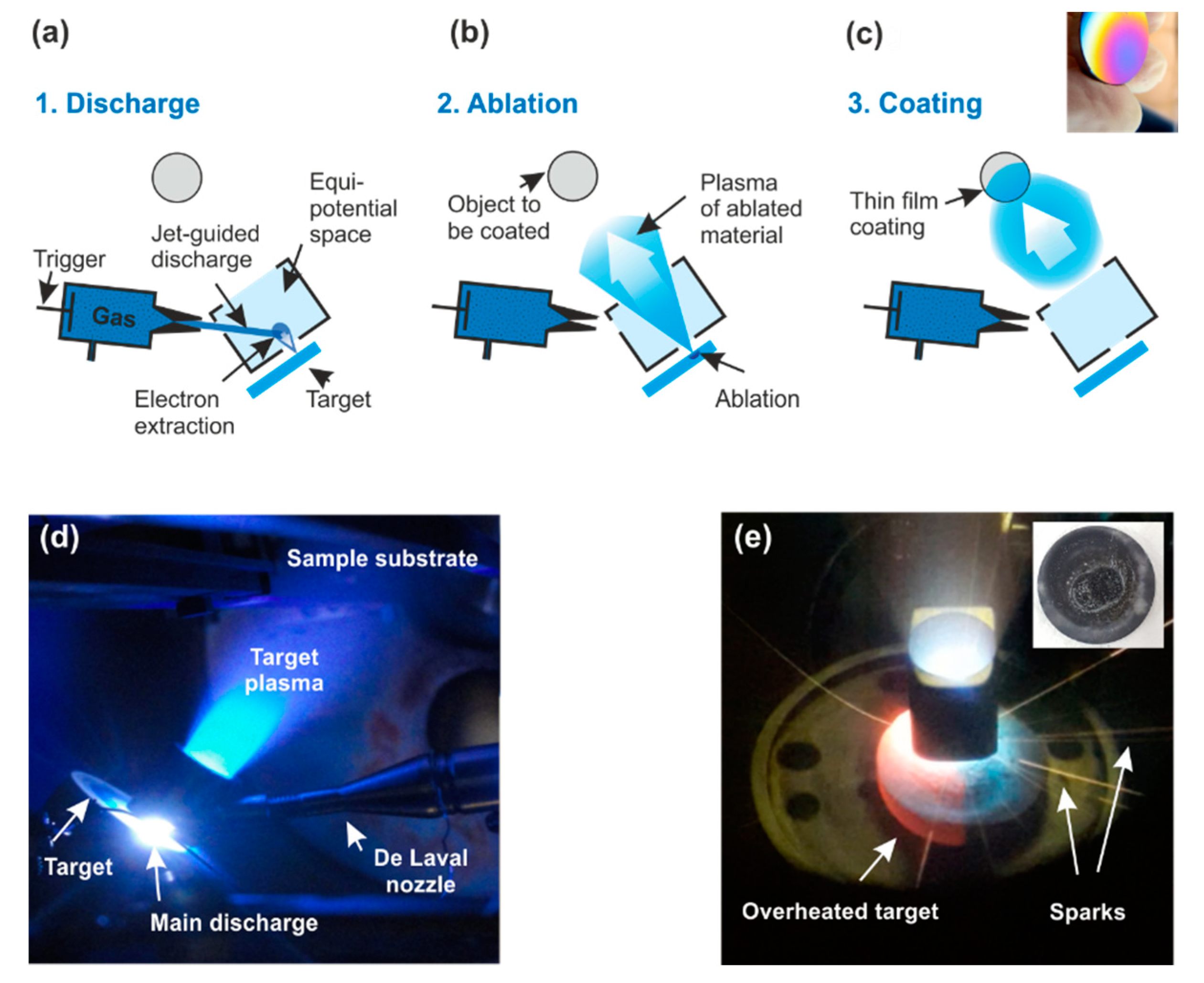
2. Materials and Methods
3. Results
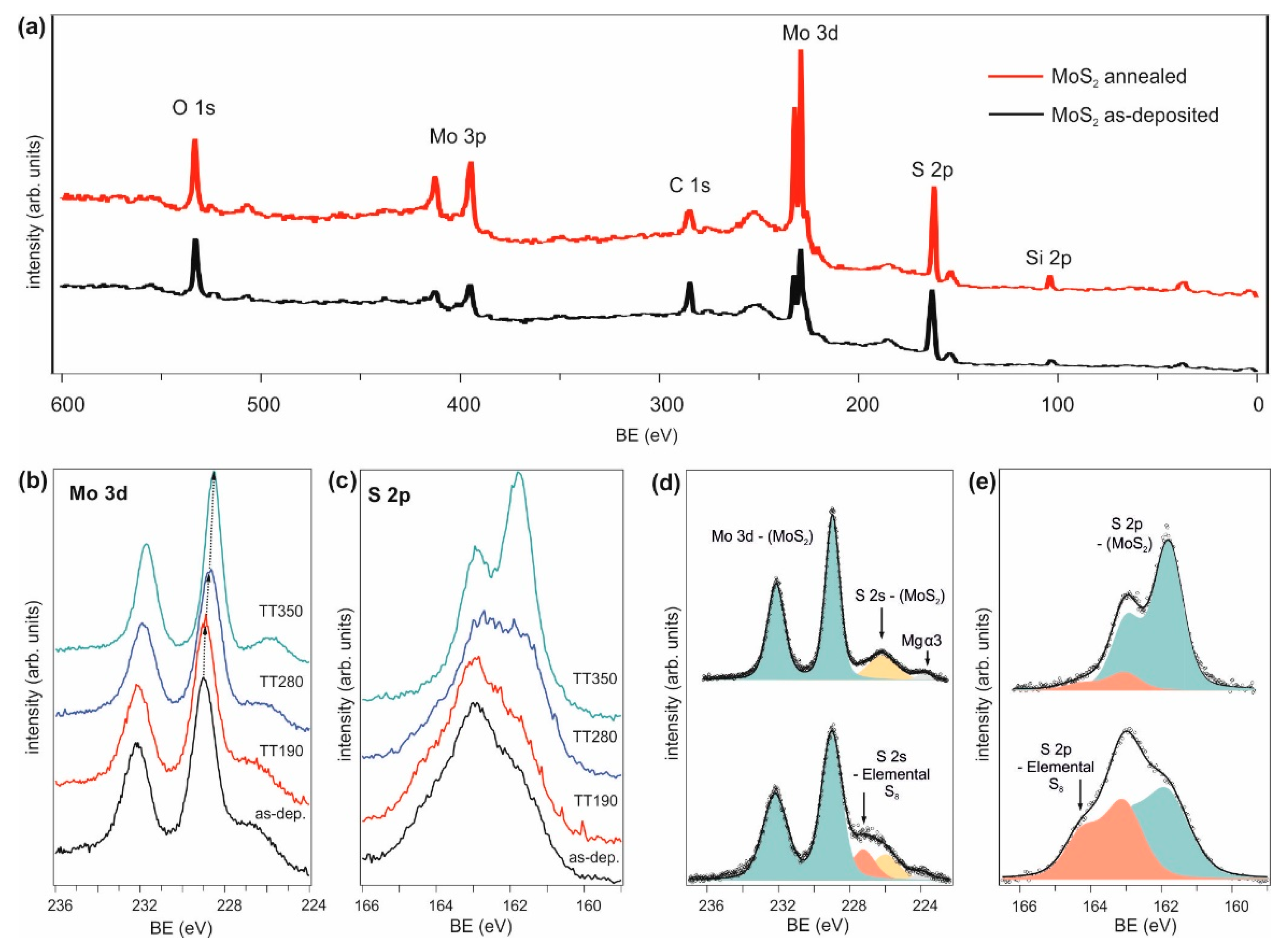
3.1. Influence of Annealing Temperature
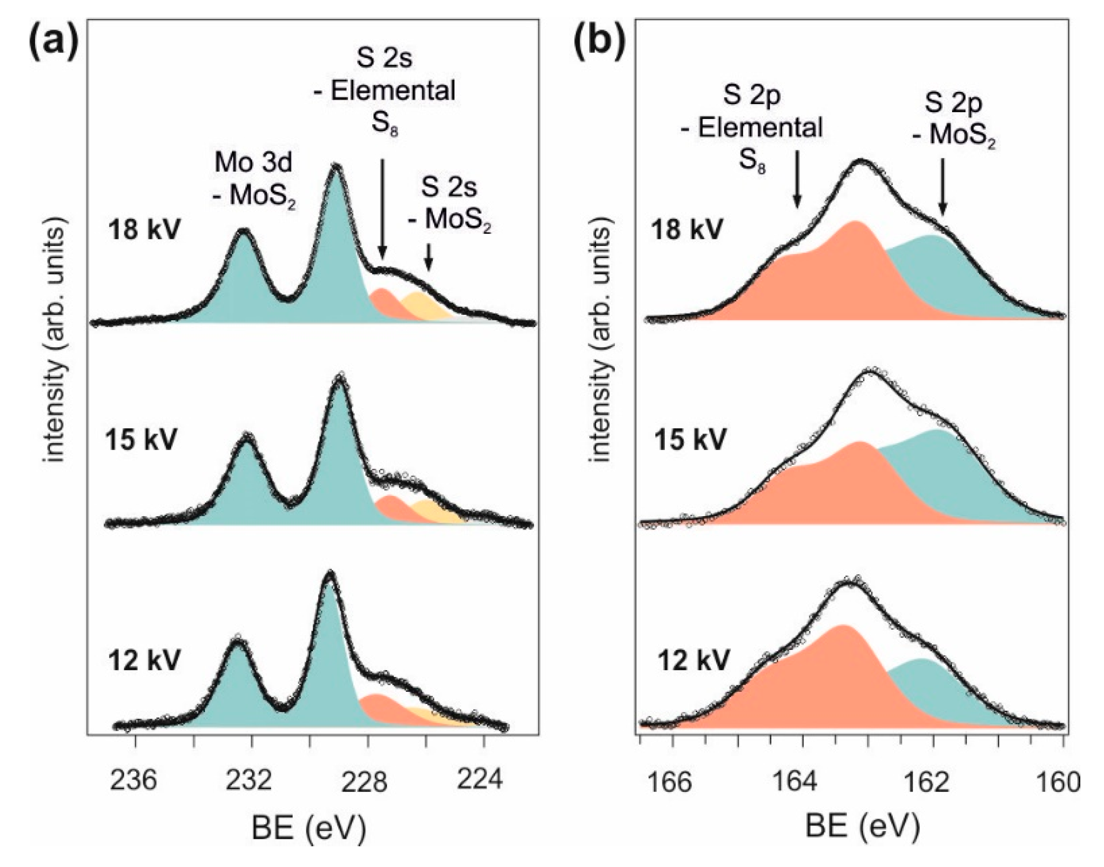
3.2. Influence of Acceleration Voltage
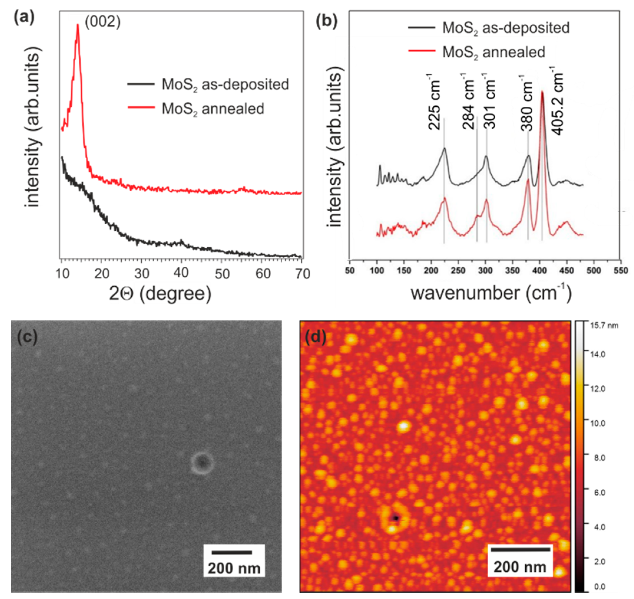
3.3. Structural and Morphological Analysis of Annealed MoS2
3.4. Role of the SiO2/Si Substrate
4. Discussion
5. Conclusions
Author Contributions
Funding
Acknowledgments
Conflicts of Interest
References
- Mak, K.F.; Lee, C.; Hone, J.; Shan, J.; Heinz, T.F. Atomically thin MoS2: A new direct-gap semiconductor. Phys. Rev. Lett. 2010, 105, 136805. [Google Scholar] [CrossRef] [PubMed]
- Samadi, M.; Sarikhani, N.; Zirak, M.; Zhang, H.; Zhang, H.; Moshfegh, A.Z. Group 6 transition metal dichalcogenide nanomaterials: Synthesis, applications and future perspectives. Nanoscale Horiz. 2018, 3, 90–204. [Google Scholar] [CrossRef] [PubMed]
- Xi, X.; Wang, Z.; Zhao, W.; Park, J.H.; Law, K.T.; Berger, H.; Forró, L.; Shan, J.; Mak, K.F. Ising pairing in superconducting NbSe2 atomic layers. Nat. Phys. 2016, 12, 139–143. [Google Scholar] [CrossRef]
- Radisavljevic, B.; Radenovic, A.; Brivio, J.; Giacometti, V.; Kis, A. Single-layer MoS2 transistors. Nat. Nanotechnol. 2011, 6, 147–150. [Google Scholar] [CrossRef] [PubMed]
- Liu, N.; Baek, J.; Kim, S.M.; Hong, S.; Hong, Y.K.; Kim, Y.S.; Kim, H.-S.; Kim, S.; Park, J. Improving the Stability of High-Performance Multilayer MoS2 Field-Effect Transistors. ACS Appl. Mater. Interfaces 2017, 9, 42943–42950. [Google Scholar] [CrossRef]
- Kim, J.S.; Yoo, H.W.; Choi, H.O.; Jung, H.T. Tunable volatile organic compounds sensor by using thiolated ligand conjugation on MoS2. Nano Lett. 2014, 14, 5941–5947. [Google Scholar] [CrossRef]
- Lee, J.; Dak, P.; Lee, Y.; Park, H.; Choi, W.; Alam, M.A.; Kim, S. Two-dimensional layered MoS₂ biosensors enable highly sensitive detection of biomolecules. Sci. Rep. 2014, 4, 7352. [Google Scholar] [CrossRef]
- Wang, W.; Panin, G.N.; Fu, X.; Zhang, L.; Ilanchezhiyan, P. MoS2 memristor with photoresistive switching. Sci. Rep. 2016, 6, 31224. [Google Scholar] [CrossRef]
- Nardi, M.V.; Timpel, M.; Ligorio, G.; Morales, N.Z.; Chiappini, A.; Toccoli, T.; Verucchi, R.; Ceccato, R.; Pasquali, L.; List-Kratochvil, E.J.W.; et al. Versatile and Scalable Strategy To Grow Sol−Gel Derived 2H-MoS2 Thin Films with Superior Electronic Properties: A Memristive Case. ACS Appl. Mater. Interfaces 2018, 10, 34392–34400. [Google Scholar] [CrossRef]
- Magda, G.Z.; Pető, J.; Dobrik, G.; Hwang, C.; Biró, L.P.; Tapasztó, L. Exfoliation of large-area transition metal chalcogenide single layers. Sci. Rep. 2015, 5, 14714. [Google Scholar] [CrossRef]
- Backes, C.; Higgins, T.M.; Kelly, A.; Boland, C.; Harvey, A.; Hanlon, D.; Coleman, J.N. Guidelines for Exfoliation, Characterization and Processing of Layered Materials Produced by Liquid Exfoliation. Chem. Mater. 2017, 29, 243–255. [Google Scholar] [CrossRef]
- Zhang, J.; Yang, A.; Wu, X.; van de Groep, J.; Tang, P.; Li, S.; Liu, B.; Shi, F.; Wan, J.; Li, Q.; et al. Reversible and selective ion intercalation through the top surface of few-layer MoS2. Nat. Commun. 2018, 9, 1–9. [Google Scholar] [CrossRef] [PubMed]
- Lee, Y.-H.; Zhang, X.-Q.; Zhang, W.; Chang, M.-T.; Lin, C.-T.; Chang, K.-D.; Yu, Y.-C.; Wang, J.T.-W.; Chang, C.-S.; Li, L.-J.; et al. Synthesis of Large-Area MoS2 Atomic Layers with Chemical Vapor Deposition. Adv. Mater. 2012, 24, 2320–2325. [Google Scholar] [CrossRef] [PubMed]
- George, A.S.; Mutlu, Z.; Ionescu, R.; Wu, R.J.; Jeong, J.S.; Bay, H.H.; Chai, Y.; Mkhoyan, K.A.; Ozkan, M.; Ozkan, C.S. Wafer scale synthesis and high resolution structural characterization of atomically thin MoS2 layers. Adv. Funct. Mater. 2014, 24, 7461–7466. [Google Scholar] [CrossRef]
- Gobbi, M.; Bonacchi, S.; Lian, J.X.; Bertolazzi, A.V.S.; Zyska, B.; Timpel, M.; Tatti, R.; Olivier, Y.; Hecht, S.; Nardi, M.V.; et al. Collective molecular switching in hybrid superlattices for light-modulated two-dimensional electronics. Nat. Commun. 2018, 9, 2661. [Google Scholar] [CrossRef]
- Siegel, G.; Venkata Subbaiah, Y.P.; Prestgard, M.C.; Tiwari, A. Growth of centimeter-scale atomically thin MoS2 films by pulsed laser deposition. APL Mater. 2015, 3, 056103. [Google Scholar] [CrossRef]
- Tao, J.; Chai, J.; Lu, X.; Wong, L.M.; Wong, T.I.; Pan, J.; Xiong, Q.; Chi, D.; Wang, S. Growth of wafer-scale MoS2 monolayer by magnetron sputtering. Nanoscale 2015, 7, 2497–2503. [Google Scholar] [CrossRef]
- Lotti, R.; Nozar, P.; Taliani, C. Device for Generating Plasma and for Directing an Flow of Electrons towards a Target. WO2010109297A2, 30 September 2010. [Google Scholar]
- Skocdopolova, L. Device for Generating Plasma and Directing an Electron Beam towards a Target. WO2013186697A3, 19 December 2013. [Google Scholar]
- Skocdopolova, L. Un Apparato ed un Metodo per la Generazione di Elettroni e di Plasma da un Getto di Gas. ITBO 20120320 A1, 11 December 2013. [Google Scholar]
- Heinrich, P.; Stoltenhoff, T.; Richter, P.; Kreye, H.; Richter, H. Method and System for Cold Gas Spraying. U.S. Patent US20040166247A1, 5 December 2006. [Google Scholar]
- Little, P.F.; von Engel, A. The hollow-cathode effect and the theory of glow discharges. Proc. R. Soc. A 1954, 224, 209–227. [Google Scholar]
- Mignuzzi, S.; Pollard, A.J.; Bonini, N.; Brennan, B.; Gilmore, I.S.; Pimenta, M.A.; Richards, D.; Roy, D. Effect of disorder on Raman scattering of single-layer MoS2. Phys. Rev. B-Condens. Matter Mater. Phys. 2015, 91, 1–7. [Google Scholar] [CrossRef]
- Li, H.; Zhang, Q.; Yap, C.C.R.; Tay, B.K.; Edwin, T.H.T.; Olivier, A.; Baillargeat, D. From bulk to monolayer MoS2: Evolution of Raman scattering. Adv. Funct. Mater. 2012, 22, 1385–1390. [Google Scholar] [CrossRef]
- Windom, B.C.; Sawyer, W.G.; Hahn, D.W. A Raman Spectroscopic Study of MoS2 and MoO3: Applications to Tribological Systems. Tribol. Lett. 2011, 42, 301–310. [Google Scholar] [CrossRef]
- Gołasa, K.; Grzeszczyk, M.; Bozek, R.; Leszczyński, P.; Wysmołek, A.; Potemski, M.; Babiński, A. Resonant Raman scattering in MoS2- From bulk to monolayer. Solid State Commun. 2014, 197, 53–56. [Google Scholar] [CrossRef]
- Morita, M.; Ohmi, T.; Hasegawa, E.; Kawakami, M.; Ohwada, M. Growth of native oxide on a silicon surface. J. Appl. Phys. 1990, 68, 1272–1281. [Google Scholar] [CrossRef]
- Song, Y.; Li, X.; Mackin, C.; Zhang, X.; Fang, W.; Palacios, T.; Zhu, H.; Kong, J. Role of interfacial oxide in high-efficiency graphene-silicon schottky barrier solar cells. Nano Lett. 2015, 15, 2104–2110. [Google Scholar] [CrossRef] [PubMed]
- Kim, S.; Kim, M.C.; Choi, S.H.; Kim, K.J.; Hwang, H.N.; Hwang, C.C. Size dependence of Si 2p core-level shift at Si nanocrystal/ SiO2 interfaces. Appl. Phys. Lett. 2007, 91, 1–4. [Google Scholar] [CrossRef]
- Renault, O.; Marlier, R.; Gely, M.; De Salvo, B.; Baron, T.; Hansson, M.; Barrett, N.T. Synchrotron radiation X-ray photoelectron spectroscopy of Si nanocrystals grown onto Al2O3/Si surfaces. Appl. Phys. Lett. 2005, 87, 163119. [Google Scholar] [CrossRef]
- Hussain, S.; Singh, J.; Vikraman, D.; Singh, A.K.; Iqbal, M.Z.; Khan, M.F.; Kumar, P.; Choi, D.C.; Song, W.; An, K.S.; et al. Large-area, continuous and high electrical performances of bilayer to few layers MoS2 fabricated by RF sputtering via post-deposition annealing method. Sci. Rep. 2016, 6, 1–13. [Google Scholar] [CrossRef]


| Sample | BE (eV) | FWHM | S/Mo 1 [2.0] | S/Mo 2 [2.0] | ||
|---|---|---|---|---|---|---|
| Mo 3d5/2 | S 2p3/2 | Mo 3d | S 2p | |||
| single crystal | 229.55 | 162.36 | 0.85 | 0.91 | 1.92 | |
| as-deposited | 228.99 | 161.86 | 1.41 | 1.52 | 3.81 | 2.11 |
| TT190 | 228.96 | 161.81 | 1.33 | 1.44 | 3.62 | 1.98 |
| TT280 | 228.72 | 161.54 | 1.30 | 1.35 | 2.88 | 1.95 |
| TT350 | 228.62 | 161.45 | 1.02 | 1.01 | 2.39 | 2.14 |
| Acceleration Voltage | Sample | BE (eV) | FWHM | S/Mo 1 [2.0] | ||
|---|---|---|---|---|---|---|
| Mo 3d5/2 | S 2p3/2 | Mo 3d | S 2p | |||
| 12 kV | as-deposited | 229.08 | 162.07 | 1.35 | 1.34 | 4.63 |
| TT400 | 228.34 | 161.92 | 0.94 | 0.98 | 2.14 | |
| 15 kV | as-deposited | 228.99 | 161.86 | 1.41 | 1.52 | 3.81 |
| TT350 | 228.62 | 161.45 | 1.02 | 1.01 | 2.39 | |
| 18 kV | as-deposited | 229.09 | 161.94 | 1.46 | 1.57 | 4.41 |
| TT380 | 228.62 | 161.45 | 1.02 | 1.01 | 2.31 | |
Publisher’s Note: MDPI stays neutral with regard to jurisdictional claims in published maps and institutional affiliations. |
© 2020 by the authors. Licensee MDPI, Basel, Switzerland. This article is an open access article distributed under the terms and conditions of the Creative Commons Attribution (CC BY) license (http://creativecommons.org/licenses/by/4.0/).
Share and Cite
Ghiami, A.; Timpel, M.; Chiappini, A.; Nardi, M.V.; Verucchi, R. Synthesis of MoS2 Thin Film by Ionized Jet Deposition: Role of Substrate and Working Parameters. Surfaces 2020, 3, 683-693. https://doi.org/10.3390/surfaces3040045
Ghiami A, Timpel M, Chiappini A, Nardi MV, Verucchi R. Synthesis of MoS2 Thin Film by Ionized Jet Deposition: Role of Substrate and Working Parameters. Surfaces. 2020; 3(4):683-693. https://doi.org/10.3390/surfaces3040045
Chicago/Turabian StyleGhiami, Amir, Melanie Timpel, Andrea Chiappini, Marco Vittorio Nardi, and Roberto Verucchi. 2020. "Synthesis of MoS2 Thin Film by Ionized Jet Deposition: Role of Substrate and Working Parameters" Surfaces 3, no. 4: 683-693. https://doi.org/10.3390/surfaces3040045
APA StyleGhiami, A., Timpel, M., Chiappini, A., Nardi, M. V., & Verucchi, R. (2020). Synthesis of MoS2 Thin Film by Ionized Jet Deposition: Role of Substrate and Working Parameters. Surfaces, 3(4), 683-693. https://doi.org/10.3390/surfaces3040045