Abstract
The self-organized formation of nanoscale laser-induced periodic surface structures (LIPSS) is still not fully understood with respect to the dynamics and interplay of contributing complex mechanisms. The transition from randomness to order and the specific role of nano-feedback are of fundamental interest because of their general aspects. In our study, the very first steps of the surface reconfiguration are demonstrated by analyzing the topology of evolving nano-crater maps. The evolution of spatial frequencies and directional arrangement indicate a feedback-driven adaptation of k-vectors to the required excitation conditions of elementary dipoles in the linearly polarized laser field. The time-dependent structure formation was studied by pump-probe diffraction and scattering experiments. The ratio of the contributions of characteristic light patterns enables plasmonic and non-plasmonic mechanisms to be distinguished, which subsequently act at distinctly different time scales. Recently developed multistage models for the dynamics of material modification are confirmed. The influence of accumulation effects is clearly demonstrated by characteristic changes in scattering and diffraction with an increasing number of preceding pulses. It is assumed that the thermal and plasmonic contributions to accumulation are coupled and thus generate spatially variable modifications.
1. Introduction
Shortly after the invention of the laser, it was reported by Milton Birnbaum that the illumination of semiconductor surfaces with intense laser radiation can lead to the generation of grating-like structures in solid surfaces [1]. Dynamic changes of the surface reflectivity were interpreted to be related to the induction of electron-holes pairs. One of the materials studied in these early experiments was silicon, which, nowadays, belongs to the most important materials in optoelectronics, photonics, photovoltaics, and many other industries. On a microscale, the structural modifications of polished silicon after laser treatment were found to consist of “numerous small pits and irregular cracks about 10−3 cm in length”. In the following years, such laser-induced periodic surface structures (LIPSS), often simply referred to as “ripples”, were obtained in many kinds of materials, including metals and isolators like glasses, ceramics, diamond, or polymers. Nanostructured materials in metals and compound structures with specific plasmonic properties are of growing interest for applications for surface-enhanced Raman spectroscopy [2], laser particle acceleration [3], photocatalysis, or as antibacterial agents [4,5], to mention only a few.
The mechanisms of LIPSS formation, however, were found to not be of a universal nature and are still often controversially discussed. They can be determined by the type and fine structure of the material, as well as by the parameters of the illuminating light (wavelength, intensity, pulse energy, pulse shape, number of pulses, polarization map, angular profile, ambient media, scanning velocity, orbital angular momentum etc.). Among the various explanations of LIPSS-formation, we find the excitation of laser-induced surface plasma waves [6,7,8,9,10], the generation of Wigner excitons [11], hydrodynamic mechanisms [12], or the thermo-mechanical relaxation of surface instabilities with material transport [13,14,15]. All of these models of laser-induced structure formation are based on immanent feedback loops in combination with self-organization mechanisms which selectively react to parameter variations.
The plasma wave model starts from statistically distributed initial scatterers which are randomly scattering in all directions in half space. The scattered light undergoes a spatial selection which is determined by the k-vector selection rules and therefore also by the spectral bandwidth. Contributions which fulfill the selection rules are promoted, whereas mismatching spatial frequency components are suppressed. The spatial acceptance characteristics are convoluted with the dipole characteristics of the scatterers, which can thus be interpreted as nano-antennas of a variable diameter [16,17]. On this basis, the generation of low-spatial-frequency LIPSS (LSFL) can be well-understood. It is furthermore assumed that, in the periodical field maxima, photoelectrons are emitted, leaving positively charged lattice parts which are locally ablated by Coulomb micro-explosions. The polarization-selectivity of the feedback leads to a subsequent narrowing of the angular spectrum so that the degree of order is increased and the ripples approximate a highly parallel orientation. Ripples are found to appear both parallel and perpendicular to the polarization vector. The responsible physics is not always the same and depends on the specific laser-material interaction scenario. For example, dynamic polarization flip effects near the plasmon resonance [18] or intrinsic frequency conversion [19] can strongly modify the orientation of the ripples. The optical feedback directly modulates the rates and efficiency of absorption and ablation by field enhancement, resonance effects, and light-redistribution [20,21]. Grating-like patterns consisting of alternating melted and solid zones were observed, which are closely related to the length scales of different optical and thermodynamically mechanisms [22]. Apart from the LSFL, the generation of high-spatial-frequency LIPSS (HSFL) with feature sizes far below the optical wavelength was reported from experiments with ultrashort-pulsed lasers [23,24,25,26,27]. The formation of this particular type of LIPSS can be attributed to alternative mechanisms like harmonic generation [19]. As we previously demonstrated, the formation of LIPSS in transparent large-bandgap materials (e.g. ZnO or TiO2) is supported by multiphoton excitation in focused highly intense laser fields [28,29]. For an appropriate explanation, the classical Drude model had to be extended by including a nonlinear term which leads to a transient metal-like state that provides the required carriers for generating surface plasmon polaritons (SPPs) [28]. The nonlinear excitation model corresponds to experimentally observed, intensity-dependent ripple periods. This was confirmed, e.g., by radially continuously varying periods for illumination with Gaussian intensity profiles [28]. The relevance of SPPs as essential contributions to the ripple generation was confirmed by several studies [30,31,32,33,34,35,36]. A strong indication of the existence of plasmonic mechanisms is the dependence of the structure formation on the polarization of the inducing laser beam [37]. Two-plasmon resonance is addressed as another possible origin of HSFL [38].
For metals like Ti, Al, and Au, it was shown that nanoscale surface boiling plays a role in sub-threshold damage, as well as above-threshold spallation by femtosecond laser pulses [39,40]. Although thermal material modification and rearrangement were detected at different time scales compared to the exciting light pulses, the ripple formation is significantly influenced by plasmons initially induced by the ultrafast laser pulses [39]. These findings indicate that a combination of sub-surface bubble generation and plasmon-related spatially periodical energy insertion results in the generation of isolated or merged nanovoids, depending on the fluence. In other words, the cooperation of non-thermal and thermal mechanisms can lead to a kind of memory effect for plasmonic spatial frequency information, which also has to be expected for the ultrafast excitation of transparent materials. This picture is further supported by observations of volume bubble formation and rearrangement in glasses which were found to be related to plasmonic mechanisms [41,42]. Recent studies of the dynamics of LIPSS formation in silicon with time- and pulse-number-resolved microscopic pump-probe reflectometry with the moving-spot approach [43,44] revealed that the generation of free electrons at a high power density leads to non-thermal melting, liquid phase overheating, and finally to a rapid solidification into the amorphous phase. In this paper, it was argued that far- and near-field scattered light interferes with the incident laser light without the need to involve surface plasmon polaritons. The results of other groups, however, provide a strong indication of plasmonic contributions [35,45]. Recent studies with nanosecond pulses also include the possibility of SPP generation [46]. In two-color double-pulse experiments, the evidence for a plasmonic origin of LIPSS generation in silicon was clearly shown [47]. Because of the existence of a critical carrier density for plasmon excitation, ultrafast excitation is required. Some phenomena like the reported independence on a variation of the angle of incidence [48] or the detailed pathways to HSFL [49] are not yet fully understood.
Pump-probe measurements can be performed, for example, with respect to spectral properties, phase, reflectivity, or surface structure. Recently, pump-probe imaging was used to study the ultrafast dynamics of LIPSS formation on gold films [50].
Here, we report on complementary femtosecond-laser experiments by (i) exploring the very early process stages by analyzing the microscale structural changes with respect to the spatial frequency evolution and the convergence of the angular characteristics of micro-craters, and (ii) analyzing the structural evolution by pump-probe scattering and diffraction measurements [20,51].The micro-crater evolution is investigated following an alternative strategy targeting self-organized spatial frequency and angular domain parameters simultaneously. Moreover, pump-probe measurements are performed with a femtosecond-range temporal resolution and two-dimensional, highly sensitive detectors.
Specific spatio-temporal changes of interference features are addressed, which indicate non-stationary plasmonic contributions. The results confirm that the LIPSS generation in silicon with near-infrared femtosecond lasers can only be explained by a hybrid model of subsequent non-thermal and thermal processes on different time scales. Moreover, systematic pulse-number-dependent measurements emphasize the role of feedback and accumulation effects for the self-organizing emergence of periodic nanostructures in silicon surfaces.
2. Experimental Techniques
Single as well as multiple pulses for illumination can be extracted from a Ti:Sapphire laser (Spitfire, Spectra Physics/Newport, central wavelength 800 nm, pulse duration 120 fs, spectral FWHM 10 nm, repetition frequency 1 kHz, typical average laser power 2.3 W, linearly polarized). The pulse sequence can be selected by the integrated laser steering software. The pulses are inserted into an extended Mach-Zehnder interferometer. The experimental setup for pump-probe scattering and diffraction measurements is schematically depicted in Figure 1. The beam splitter generates two partial beams by transmitting 20% and reflecting 80% of the original pulse power. The first optical path (including mirrors M1 and M2) guides the reflected contribution as the pump beam to the silicon specimen. The pulse power is adjusted by a rotatable half wave plate, which acts as a polarization analyzer. A cylindrical lens (L1, f = 100 mm) focuses the pump beam onto the surface of the silicon specimen. The second part of the light (transmitted at the beam splitter) is frequency converted by second harmonic generation (SHG) in a beta barium borate (BBO) crystal. The frequency doubled (400 nm) pulses are used as probe pulses at low (sub-threshold) fluence values to avoid parasitic short-wavelength-induced ripples. The time delay between the pump and probe pulses can be adjusted by varying the distance between mirrors M1 and M2. After being reflected at Mirror M6, the probe beam is focused by a spherical lens (f = 100 mm) and hits the surface at an angle of 15° with respect to the normal incidence. The diffusely scattered and diffracted light reaches a screen which is imaged onto a single-photon capable, 2D electron multiplying charge coupled device (EMCCD) camera (iXon, Andor, LOT).
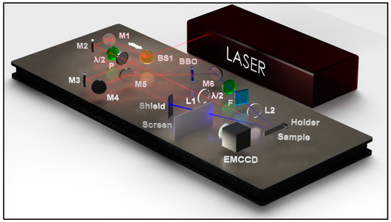
Figure 1.
Pump-probe configuration for the time-dependent characterization of femtosecond laser-induced LIPSS in silicon/air (BS1: 80/20 beam splitter, M1-M6: HR mirrors, L1: f = 100 mm cylindrical lens, L2: f = 100 mm spherical lens, λ/2: half wave plates, P: linear polarizers, BBO: beta barium borate crystal for second harmonic generation, F: BG39 color glass filter, EMCCD: 2D electron multiplying charge coupled device camera).
To enhance the contrast, the specular reflection of the probe beam is suppressed by guiding it through a pinhole in the screen on a beam trap (shield). The spatial and temporal coincidence of pump and probe beams was roughly pre-adjusted by detecting the non-collinear (SHG) intensity cross-correlation signal generated by a second BBO crystal with a photodiode. For fine adjustment, a ZnO nanolayer (thickness about 300 nm) was used for the frequency conversion, thus enabling optimization of the spatio-temporal overlap with a high resolution and the definition of the zero temporal delay state.
The intensity profile of the pump beam was measured with a beam profiler (M 100, Metrolux, Göttingen, Germany). At a maximum pump power of 1.2 W, a maximum intensity of 2.13 TW/cm2 and a fluence of 0.55 J/cm2 in the focal spot were obtained, whereas the probe pulse intensity was estimated to be 18 times lower. Surface structures in silicon were inspected with a high-resolution field-emission scanning electron microscope (FE-SEM, JEOL JSM-6400F, JEOL GmbH, Freising, Germany), including energy dispersive X-Ray Spectroscopy (EDS). A spatial frequency analysis of SEM images was performed by two-dimensional Fast Fourier Transform (FFT).
3. Material Properties
To enable a plasmonic contribution to LIPSS formation, two preconditions have to be fulfilled: (1) The material has to be capable of generating enough free carriers, and (2) coupling of light into the plasmons has to be enabled by an appropriate re-distribution mechanism (scattering). Furthermore, possible transitions from crystalline to amorphous Si require the involvement of specific material parameters for both states. In the following, related electronic and optical properties are discussed on the basis of a simplified model which enables a qualitative description of the pre-conditions of the laser-material interaction processes. It should be noticed that, in order to evaluate the material properties at maximum fluence, we considered peak values for the carrier density corresponding to constant optical parameters like reflectivity. It is clear that, for dynamic modelling, most optical parameters have to be assumed to be time-dependent, as shown in detail in the literature [36,44,52,53,54,55]. The difficulty for any realistic confinement of the modelling is the high complexity of the mechanisms, including dynamic feedback. One has to expect not only a transient change of the optical parameters with the carrier density, but also changes by eliminating thin oxide layers in the initial stage, amorphization after melting and re-solidification, the accumulation of defects, and changes induced by the evolving nanostructures. In particular, the optical action of the growing nanostructures opens selective feedback channels by diffraction and enhancement, which can be studied by pump-probe diffraction and scattering experiments.
3.1. Crystalline Silicon
Pump-probe experiments were performed with phosphorus-doped crystalline <100> silicon wafers. The specific resistance of 0.1 to 2 Ω cm (data from CrysTec) corresponds to carrier densities in the range of 8.35 × 1016 cm−3 to 2.36 × 1015 cm−3. At a central wavelength of λ0 = 800 nm, room temperature, and the given crystal orientation, the complex dielectric function εSi and the complex refractive index nSi of n-doped Si are found to be [54]
where εSi’ and εSi’’are the real and imaginary part of the dielectric function, respectively, and nSi,real and kSi are the real part of the refractive index and extinction coefficient, respectively. For λ0, a linear absorption coefficient of αSi = 942.48 cm−1 can be calculated on this basis. The (low intensity) reflectivity at normal incidence is RSi = 0.328 at the central laser wavelength. The two-photon absorption coefficient is in the range of βSi = 6.8 × 10⁻¹¹ m/W [55]. Assuming that the number of excited electrons ne equals the number of donors, one can roughly estimate ne for a wavelength of λ0 = 800 nm, a pulse duration of τ = 120 fs, and a peak fluence of Φ0 = 0.55 J/cm2 via the following relationship (after [45]):
where (hν = photon energy at λ0 = 800 nm) has to be in the order of 7.51 × 1021 cm−3.
It has to be noticed that the estimation is related to unexcited material and the pulse absorption is regarded as instantaneous. In a more realistic model, the time dependence of the parameters has to be taken into account. The effective optical mass of the carriers for moderately doped n-Si with an excited state carrier density in the conduction band of about 5 × 1021 cm−3 is reported to be mopt,n-Si = 0.57 me (me = rest mass of the electron) [56]. With the plasma frequency
(ε0 = vacuum permittivity), the angular frequency
(c = vacuum velocity of light), and the dielectric function of a Drude-Sommerfeld metal (here: highly excited transient metallic silicon [57]
and after complex conjugation and inserting the Drude collision time in n-Si, τD,n-Si = 4.1 × 10⁻¹⁵ s, one ends up with the real and imaginary parts:
The term ε∞ describes the dielectric function of the positive ion background, which can be neglected if the effects of free carriers dominate [58]. In our case, this condition is fulfilled (ε∞ = 1), so the influence on the plasma frequency in Equation (4) is cancelled out. The transient, complex dielectric function of n-Si can therefore be written as
On the basis of different confined theoretical models for the transient optical properties of ultrafast excited silicon, the complex material response was quantitatively predicted in the literature [36,53].
In particular, the reflectivity is expected to have a maximum and the impact ionization coefficient should depend nonlinearly on the laser intensity [53]. Lifetimes of modified optical states are calculated to be in the order of a few tens of femtoseconds. Minimum reflectivity indicates the transition to metallization and the achievement of the ionization threshold. The simulations basically confirm that the electronic material properties support the generation of SPPs. The interference mechanisms (light, SPPs and SPPs, SPPs and light, SPP recombination), however, are still much debated. Observations suggest that multiple mechanisms can act in a complex scenario, depending on dynamic material parameters and non-stationary excitation conditions.
Studies of few-pulse modification of subsurface morphology suggest that the initial phase is significantly defined by defect generation [59] and incubation [60].
3.2. Amorphous Silicon
The amorphization of crystalline Si is known to be an essential contribution to the scenario of LIPSS formation [45,61]. At fluences well below the single pulse ablation threshold, a shock wave propagates along the surface, which leads to melting and which is followed by re-solidification into a layer of amorphous material (a-Si) with a parabolic profile with a depth of a few tens’ nm [45]. For unexcited amorphous Si, the dielectric function at the laser wavelength and the complex refractive index are [62]
The linear absorption coefficient
can be estimated to be αa-Si = 17.122 cm−1. The two-photon absorption coefficient of amorphous Si of βa-Si = 3.7 × 10⁻¹⁰ m/W [63] delivers an effective optical mass of mopt,a-Si = 0.18 × me and a Drude collision time of τD,a-Si = 1 × 10⁻¹⁵ s. The reflectivity at normal incidence is Ra-Si = 0.35. With the help of these parameters and Equations (3) and (4), it follows that
The transient, complex dielectric function of a-Si can be calculated on the basis of Equations (7) and (8):
The evaluation of the calculated material functions is part of the section with experimental results.
4. Spatial Frequencies and Plasmon Coupling
For the coupling of a photon to a surface plasmon, only k-vector components parallel to the surface with polarization parallel to the plane of incidence are necessary. From the dispersion relations for SPPs, however, it follows that this component does not exist for perfectly smooth surfaces [64]. Nonradiative plasmons in both thin and thick films, however, can couple to electromagnetic radiation in the presence of surface roughness or by means of a grating [65]. With increasing roughness, the spatial frequency spectrum of a surface contains more components which match the coupling condition. On the other hand, increasing losses by scattering and beam distortion may work against this tendency so that one has to expect the existence of an optimum spatial frequency with optimum (center of gravity) angular characteristics determined by the polarization vector. A grating as a coupler provides the required momentum matching by enhancing the transversal k-vector component by multiples of 2π/kgrating [66]. The coupling behavior was experimentally demonstrated for gratings with typical LIPSS periods [32]. The role of micro-craters in the initial phase of LIPSS formation in Si was investigated for femtosecond laser irradiation at fluences in a few J/cm2 range [45]. It was shown that after the first pulse, a random distribution of craters with diameters in the range of 0.5–5 µm appears. The spatial density and size of the craters is obviously influenced by beam hot spots and local material inhomogeneities. Fringe-like sub-structures around certain (but not all) craters indicate (a) the dipole-like, polarization-dependent generation of SPPs, which is (b) preferentially found around craters of a selected size and/or inner structure, obviously for best matching spatial frequency components. This goes well with the assumptions on the existence of optimum conditions for spatial and angular selection resulting from laser spectrum, polarization, and dielectric function.
5. Results and Discussion
5.1. Dynamic Initial Feedback Mechanism
5.1.1. Micro-craters
Building on previous findings on the crucial role of initial roughness for starting the generation of LIPSS and spatially filtering SPPs [67], and, in particular, on the random formation of craters by micro-explosions including non-thermal melting [45,68], we investigated the temporal aspects of self-organized, feedback-driven surface modification at the very beginning of the laser-material interaction (pre-LIPSS stage). The distribution of craters after defined numbers of laser pulses with known intensity profiles was detected by SEM. Peak intensity and peak fluence at the angle of incidence of 0.42° (due to focus) were chosen to be 2.13 TW/cm2 and 0.55 J/cm2, respectively. After irradiation with a pulse number of N = 1, statistically distributed craters with an average diameter of dcrater = 0.37 µm were found. In the center of the beam profile (higher intensity), a more distinct deviation from randomness towards an ordered configuration was found (Figure 2). The initial crater formation is also (slightly) influenced by the existence of a thin (few nm) oxide layer on top, which is later blown away. This cover layer provides a certain amount of a-Si [45,61], which has to be taken into account for quantitatively simulating the metallization and losses after the first pulse.
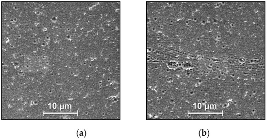
Figure 2.
Initial micro-craters in silicon after N = 1 pulses (central wavelength: 800 nm, peak intensity: 2.13 TW/cm2): (a) outer rim and (b) center of the ablation area. The degree of spatial order increases towards a higher intensity.
For identical pulse power, a tendency towards ordered structures was also observed with increasing pulse number. This tendency was confirmed by two-dimensional Fast Fourier Transform (2D-FFT).
5.1.2. Distance Function and Angular Characteristics
A more detailed, quantitative analysis was performed by adapted image processing software, programmed in Visual Basic for Applications and Excel. The algorithm calculates, for a selected field of (up to 150) micro-craters, the scatterer distances and the corresponding direction angles for all connecting lines between the centers of gravity (schematically in Figure 3).
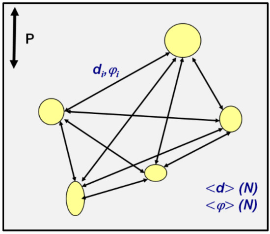
Figure 3.
Analysis principle implemented in the image processing software for studying the evolution of maps of micro-craters (yellow circles and ellipses) (schematically). The main geometrical parameters are the center-to-center scatterer distances D and the direction angle φ relative to the orientation of the polarization vector (double arrow). Averaged values <D> and <φ> are obtained as a function of the number of pulses N. After that procedure, the program sorts the distances into (73) angular intervals so that the data can be plotted in a polar plot. Figure 4 shows the evolution of <D> and <φ> for crater maps induced by N = 1, 2, 6, and 10 pulses, respectively.
Experimental data for spatial micro-crater maps derived for different pulse numbers are analyzed in Figure 4. The arrows in the polar plots provide information on both (a) the mean distance <D> between neighboring craters, and the mean direction angle <φ> (according to the scheme in Figure 3). For pulse numbers N > 1, new craters obviously overwrite old craters. With increasing intensity, the distance vector components normal to the polarization vector decrease systematically. This continues until the average center-center distance of neighboring craters gcrater in a normal direction reaches about twice the average crater diameter (gcrater = 0.75 µm ≈ 2 dcrater). The directionality with respect to the polarization agrees with findings published in ref. [45]. The reconfiguration of crater maps leads to a more efficient feedback by generating new spatial frequency components and by creating point gratings with an optimum orientation with respect to the polarization, both favoring the generation of SPPs. The dimensions of the craters can be compared with simple estimations. At normal incidence, the SPP wavelengths for n-Si and a-Si can be calculated to be 736 nm and 797 nm, respectively. For sinusoidal plasmons, the corresponding half periods have dimensions of about 368 nm and 398 nm, respectively. The value for n-Si is very close to the observed crater geometry. It can be summarized that, under the given experimental conditions, (a) the scatterer geometry is nonstationary and self-organized via polarization driven feedback, and (b) the directional and spatial-frequency adaptation to optimum SPP-coupling is relatively fast (here, it takes 10 pulses to perfectly match, at most).
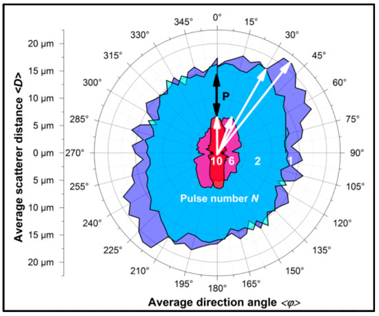
Figure 4.
Evolution of micro-crater maps in Si during the initial phase of LIPSS formation characterized by average scatterer distance <D> and average direction angle <φ>. Numbers inside filled areas stand for N = 1, 2, 6, and 10 (linearly polarized) laser pulses (black double arrow: polarization vector). The spatial frequency increases, whereas the angular orientation stepwise approaches the polarization direction.
5.2. Pump-Probe Scattering and Diffraction
5.2.1. Measuring Conditions
In contrast to previously reported pump-probe diffraction experiments [69] where the scattered signal was detected by a photo diode, we used a highly sensitive EMCCD camera as a detector, which allowed us to simultaneously monitor the two-dimensional intensity patterns and thus to extract specific spatial image information. The optical delay range of the automated measurement was limited by the maximum interferometer arm length to 30 ps. For comparing measurements at a larger time difference (2 s), the path was adjusted by hand. The pump and probe pulse had, in good approximation, Gaussian temporal-shape functions with FWHM values of 120 fs and 85 fs, respectively. The foot-to-foot time duration of the pump pulse is > 300 fs. All pump-probe measurements were performed at initial pump and probe peak intensities of 2.13 TW/cm2 and 0.12 TW/cm2, respectively, with a minimum step width of 30 fs delay. After taking into account reflection losses at normal incidence and an angle of 15°, these intensities reduce to 1.43 TW/cm2 and 0.06 TW/cm2, respectively. The probe beam was inserted with perpendicular polarization relative to the plane of incidence. By subtracting a background image from a single probe pulse reflected at pristine silicon, the linear influences on the measurement were eliminated. All images represent the same field of view on the screen (angular range from 1° to 47° from right to left in the following figures, in relation to the probe reflex which is located at the right edge). To avoid optical distortions, the sample, screen, and EMCCD had a parallel orientation. In the following, we present experimental data on two cases with N = 1, N = 2, and N = 3 pulses. One should notice that the zero time delay (Δt = 0 fs) corresponds to the exact overlap of pump and probe peaks, i.e., the starting point is the time of maximum pump intensity.
5.2.2. Initial Pulse (N = 1)
Detected scattering patterns for 15 selected time intervals between 30 fs and 2s are presented in Figure A1 (Appendix A) for a field of view of 14 × 14 cm2. Within the first 1000 fs, no significant scattering or diffraction effects are observed. The contrast of possible plasmonic field amplitudes from the pristine silicon wafer surface, if there are some, is too low to be detected. At a time difference Δt = 30 ps, slightly enhanced scattering becomes visible. The related crater formation at this time corresponds to structures as shown in Figure 2a,b and should mostly have a non-thermal origin. The mechanism behind this can be explained as follows. As shown in the introduction, the dielectric function of silicon can be changed to be negative. This enables plasmon modes which transfer energy to the lattice, finally leading to a melt with periodical electron plasma in the upper surface planes. Within the surface melt, extremely hot electrons appear (compared to the average electron temperature in the melt) that can cause nano-explosions or phase explosions [70] and bubbles. The SEM images show residual material deposition (debris) in the proximity of the craters, which can be traced back to the bursts of the bubbles. In a transiently liquid material, the bubbles are able to move. If most energy is deposited in periodical zones perpendicular to the plasmon propagation direction, most bubbles should be collected there. Such a mechanism would explain the beginning orientation of the scatterers after a single pulse (see Figure 2b). This picture is also supported by other studies on metals and dielectrics. Corresponding mechanisms were discussed for Ag, Au, and Ti under high fluence excitation [39,40], and for volume structures in glasses [42,71] (where surface plasmons, however, may be replaced by the coupling of many local plasmons). The ripple formation at the surface of fused silica is explained by the interplay of plasmons and incubation effects (accumulation of defect sites) [72].
5.2.3. Pulse Number N = 2
In Figure A2 (Appendix B), the time evolution for N = 2 is plotted. After 30 fs, modifications of the optical functions start, which are indicated by temporarily changing brightness. Between 120 fs and 210 fs, interference patterns appear, which are (with high probability) caused by SPPs. Parallel to these plasmon dynamics, a further change in brightness is also observed. After 5 ps, a weak indication of contributions by diffraction becomes visible. Such a time conforms with data from the literature [73]. These contributions manifest over the subsequent time intervals until the diffraction pattern has a high contrast on the ns-scale (see the last image in Figure A2 for 2 s). The interval of diffraction angles reaches from 33.8° to 46.4° (averaged angle: 40.1°). This corresponds to a range of spatial ripple periods between 704 nm and 791 nm (period related to the averaged angle: 741 nm). These values are related to LSFL structures. HSFLs are not resolved by the pump-probe setup. High-frequency SPPs, however, can be indicated by low-frequency beatings of interference patterns. Furthermore, we would like to address that between 120 fs and 210 fs, a rotation of the interference stripes can be seen. It can be assumed that counter-propagating plasmon modes interfere with an angular dynamic influenced by the micro-crater map. To evaluate the time interval for plasmonic activity in comparison to our experimental findings, we estimated the SPP travel time based on the Drude model, including losses from metallic and dielectric Si, and considered different phases of Si (see introductory part). For excited n-Si, a characteristic lifetime of 46 fs was theoretically calculated. For excited a-Si, the lifetime was estimated to be 298 fs (assuming a layer thickness of 60 nm in agreement with refs. [41,57]). These values represent the lower and upper limits for SPP lifetimes. This temporal range was verified by the behavior detected in the experiment (interval from 120 fs to 210 fs).
5.2.4. Pulse Number N = 3
The experiments for N = 3 (Appendix C, Figure A3) show that, induced by the ripples from the preceding first two pulses, a distinct diffraction pattern remains visible after the third pulse. The above mentioned changes in visibility (see N = 2) are again observed. At 120 fs, weak interference is still recognizable. Moreover, measurements with smaller step widths indicated that the behavior in this time regime depends sensitively on small variations in the homogeneity of the material (not shown here). This is a further hint to the presence of a plasmonic mechanism. The diffraction is accompanied by an increase of the scattered, unstructured contribution (right side of the images). We explain this observation by an additional induction of bubbles or craters in the crests of the ripples (which correspond to the areas of minimum SPP field strengths). In these areas, non-thermal processes may be less erased by thermal processes during the first few pulses.
6. Conclusions
To conclude, the dynamics of femtosecond-laser-induced ripple formation in silicon surfaces was studied with particular emphasis on structural changes and feedback. The analysis of the very initial stages confirms a self-organized reconfiguration of micro-crater maps towards adapted spatial frequencies and grating directionality. In contrast to previous publications [41], this strategy was enabled by a detailed pre-analysis of pulse-number-resolved SEM micrographs with adapted image processing software. Theoretical considerations concerning the material parameters show, in good agreement with other studies in the literature, the realistic potential for an efficient excitation of SPPs. This was well-confirmed by the results of femtosecond pump-probe experiments, extending the capabilities of previously applied techniques [49] to a higher temporal resolution and 2D spatial detection by a single-photon-sensitive EMCCD matrix camera. The observation of distinct and evolving interference patterns clearly indicates a plasmonic contribution mainly during the excitation pulse, followed by a thermal reconfiguration process at a picosecond to nanosecond time scale. In contradiction to some alternative assumptions which either exclude the influence of plasmons or, vice versa, reduce the mechanism to an interference effect, our findings give a strong indication for a more complex hybrid mechanism. Under the conditions of our experiments, the complete LIPSS formation scenario has to be regarded as a combination of non-thermal and thermal processes where the SPPs are responsible for a reconfiguration of nano-bubbles along a grating geometry and the thermal part provides the required mobility by melting the material. The pre-analysis of pulse-number-resolved micro-crater maps at equal fluence compared to the diffraction experiments allows the assumptions on local material modifications (field-induced bubbles, melting etc. [68,71]) to be transferred to the LIPSS formation scenario. The relevance of accumulation effects is underlined by the pulse number dependence [74]. The model of LIPSS formation can be described by three regimes [20]: (I) plasmon regime (free electron generation, electron heating), (II) structure regime (nonthermal melting, electron-lattice heating), and (III) stabilization regime (thermal melting, ablation, resolidification), which dominate the dynamics at different time scales (0–250 fs, 250–100 ps, 100 ps–2 ns). In all regimes, the feedback enhances with increasing pulse number, which leads to more distinct diffraction patterns. During the plasmon regime (I), an increasing degree of order of craters is obtained by field-induced micro-explosions and non-thermal melting together with polarization-related feedback. This favors SPPs interference by overcoming the wave vector discrepancy. The progressing reconfiguration of scattering craters in the earliest stage of the plasmon regime (I) was clearly demonstrated. Energy investment within the maxima of SPP interference fringes can lead to an enhanced formation of bubbles. Merging of bubbles along temporally elastic stripes of maximum carrier density requires thermal melting, which is obtained in the structure regime (II) when the transfer of electronic energy to the lattice is completed. The stabilization regime (III) is finished after 1–2 ns, i.e., long after the end of the pump pulse. The different regimes can be clearly seen in the temporally resolved 2D scattering/diffraction patterns in Figure A1, Figure A2 and Figure A3. All findings support our basic statement about the central role of feedback-driven self-organization for LIPSS generation by femtosecond-laser irradiation of polished crystalline silicon.
It is expected that the efficiency and topology of feedback and SPP formation can strongly be supported by controlling the geometrical boundary conditions, e.g., by resonant gratings or waveguiding structures. Further improvements of the spatio-temporal resolution could be obtained by applying adapted deconvolution and image recognition algorithms, photoelectron emission spectroscopy, or time resolved x-ray scattering.
Author Contributions
Both authors equally contributed to the concept, measurements, and writing and editing of the manuscript.
Funding
This research was funded by Deutsche Forschungsgemeinschaft (DFG), grant numbers GR 1782/12-1 and GR 1782/12-2.
Acknowledgments
We acknowledge stimulating discussions and support by T. Elsaesser, A. Rosenfeld†, M. Tischer, C. Patzek (MBI, Berlin), S.K. Das (KIIT University, Bhubaneswar), J. Bonse (BAM, Berlin), E. McGlynn (Dublin City University, Dublin), F. Güell (University Barcelona), and S. Höhm (Corning Laser Technologies).
Conflicts of Interest
The authors declare no conflict of interest.
Appendix A. Pump-Probe Scattering and Diffraction for N = 1

Figure A1.
Spatially resolved intensity patterns detected by pump-probe scattering after irradiating silicon in air by a single pulse (N = 1) of a Ti:Sapphire laser (central wavelength: 800 nm; pulse FWHM: 120 fs; effective peak intensities of pump and probe pulses after subtracting losses: 1.43 TW/cm2 and 0.06 TW/cm2, respectively; field of view: 14 × 14 cm2). Varying optical functions modulate the visibility temporarily. No distinct diffraction effect is observed up to the maximum time difference of 2 s.
Appendix B. Pump-Probe Scattering and Diffraction for N = 2

Figure A2.
Spatially resolved intensity patterns detected by pump-probe scattering after irradiating silicon in air by three pulses (N = 2) of a Ti:Sapphire laser (central wavelength: 800 nm; pulse FWHM: 120 fs; effective peak intensities of pump and probe pulses after subtracting losses: 1.43 TW/cm2 and 0.06 TW/cm2, respectively; field of view: 14 × 14 cm2). Three effects are observed: (1) varying optical functions modulate the visibility temporarily; (2) between 120 and 210 fs, interference indicates plasmonic contributions; and (3) distinct diffraction is observed after 2s.
Appendix C. Pump-Probe Scattering and Diffraction for N = 3

Figure A3.
Spatially resolved intensity patterns detected by pump-probe scattering after irradiating silicon in air by three pulses (N = 3) of a Ti:Sapphire laser (central wavelength: 800 nm; pulse FWHM: 120 fs; effective peak intensities of pump and probe pulses after subtracting losses: 1.43 TW/cm2 and 0.06 TW/cm2, respectively; field of view: 14 × 14 cm2). As in Figure A2 and Figure A3, varying optical functions modulate the visibility temporarily. Distinct diffraction is observed in all images.
References
- Birnbaum, M. Semiconductor surface damage produced by Ruby lasers. J. Appl. Phys. 1965, 36, 3688–3689. [Google Scholar] [CrossRef]
- Messaoudi, H.; Das, S.K.; Lange, J.; Heinrich, F.; Schrader, S.; Frohme, M.; Grunwald, R. Femtosecond-laser induced periodic surface structures for surface enhanced Raman spectroscopy of biomolecules. In Progress in Nonlinear Nano-Optics; Sakabe, M., Lienau, C., Grunwald, R., Eds.; Springer: Berlin, Germany, 2015; pp. 207–219. [Google Scholar]
- Lübcke, A.; Andreev, A.A.; Höhm, S.; Grunwald, R.; Ehrentraut, L.; Schnürer, M. Prospects of target nanostructuring for laser proton acceleration. Sci. Rep. 2017, 7, 44030. [Google Scholar] [CrossRef]
- Khan, M.E.; Khan, M.M.; Cho, M.H. Recent progress of metal–graphene nanostructures in photocatalysis. Nanoscale 2018, 10, 9427–9440. [Google Scholar] [CrossRef]
- Khan, M.E.; Han, T.H.; Khan, M.M.; Karim, M.R.; Cho, M.H. Environmentally Sustainable Fabrication of Ag@g-C3N4 Nanostructures and Their Multifunctional Efficacy as Antibacterial Agents and Photocatalysts. ACS Appl. Nano Mater. 2018, 1, 2912–2922. [Google Scholar] [CrossRef]
- Bonse, J.; Höhm, S.; Kirner, S.V.; Rosenfeld, A.; Krüger, J. Laser-induced periodic surface structures—A scientific evergreen. IEEE J. Sel. Top. Quantum Electron. 2017, 23, 9000615. [Google Scholar] [CrossRef]
- Sipe, J.E.; Young, J.F.; Preston, J.S.; van Driel, H.M. Laser-induced periodic surface structure. I. Theory. Phys. Rev. B 1983, 27, 1141–1154. [Google Scholar] [CrossRef]
- Young, J.F.; Preston, J.S.; van Driel, H.M.; Sipe, J.E. Laser-induced periodic surface structure. II Experiments on Ge, Si, Al, and brass. Phys. Rev. B 1983, 27, 1155–1172. [Google Scholar] [CrossRef]
- Young, J.F.; Sipe, J.E.; Driel, H.M. Laser-induced periodic surface structure. III. Fluence regimes, the role of feedback, and details of the induced topography in germanium. Phys. Rev. B 1984, 30, 2001–2015. [Google Scholar] [CrossRef]
- Brueck, S.R.; Ehrlich, D.J. Simulated surface plasma-wave scattering and growth of a periodic structure in laser-photodeposited metal films. Phys. Rev. Lett. 1982, 48, 1678–1681. [Google Scholar] [CrossRef]
- Kaplan, A.E.; Miyazaki, K. Laser-induced surface nano-ripples as manifestation of Wigner excitons. In Proceedings of the Quantum Electronics and Laser Science Conference (QELS), Baltimore, MD, USA, 6–11 May 2007. [Google Scholar]
- Tsibidis, G.D.; Fotakis, C.; Stratakis, E. From ripples to spikes: A hydrodynamical mechanism to interpret femtosecond laser-induced self-assembles structures. Phys. Rev. B 2015, 92, 041405(R). [Google Scholar] [CrossRef]
- Costache, F.; Eckert, S.; Reif, J. On ultra-short laser pulse induced instabilities at the surface of non-metallic solids. Proc. SPIE 2006, 6261, 626107. [Google Scholar]
- Varlamova, O. Self-Organized Surface Patterns Originating from Femtosecond Laser-Induced Instability. Ph.D. Thesis, Technical University, Cottbus, Germany, November 2013. [Google Scholar]
- Reif, J.; Costache, F.; Henyk, M.; Pandelov, S.V. Ripples revisited: Non-classical morphology at the bottom of femtosecond laser ablation craters in transparent dielectrics. Appl. Surf. Sci. 2002, 197–198, 891–895. [Google Scholar] [CrossRef]
- Csete, M.; Hild, S.; Plettl, A.; Ziemann, P.; Bor, Z.; Marti, O. The role of original surface roughness in laser-induced periodic surface structure formation process on polycarbonate films. Thin Solid Films 2004, 453–454, 114–120. [Google Scholar] [CrossRef]
- Obara, G.; Maeda, N.; Miyanishi, T.; Terakawa, M.; Nedyalkov, N.N.; Obara, M. Plasmonic and Mie scattering control of far-field interference for regular ripple formation on various material substrates. Opt. Express 2011, 19, 19093–19103. [Google Scholar] [CrossRef]
- Kudryashov, S.I.; Makarov, S.V.; Ionin, A.A.; Nathala, C.S.R.; Ajami, A.; Ganz, T.; Assion, A.; Husinsky, W. Dynamic polarization flip in nanoripples on photoexcited Ti surface near its surface plasmon resonance. Opt. Lett. 2015, 40, 4967–4970. [Google Scholar] [CrossRef]
- Dufft, D.; Rosenfeld, A.; Das, S.K.; Grunwald, R.; Bonse, J. Femtosecond laser-induced periodic surface structures revisited: A comparative study on ZnO. J. Appl. Phys. 2009, 105, 034908. [Google Scholar] [CrossRef]
- Lübcke, A.; Schnürer, M.; Ehrentraut, L.; McGlynn, E.; Byrne, D.; Lowry, S.; Wehner, R.; Grunwald, R. Interaction of ultrafast laser pulses with nanostructure surfaces. In Encyclopedia of Interfacial Chemistry: Surface Science and Electrochemistry; Wandelt, K., Ed.; Elsevier: Oxford, UK, 2018; Volume 2, pp. 420–432. [Google Scholar]
- Bonse, J.; Rosenfeld, A.; Krüger, J. Femtosecond laser-induced periodic surface structures: Recent approaches to explain, their sub-wavelength periodicities. Proc. SPIE 2012, 7994, 79940M-7. [Google Scholar]
- Van Driel, H.M.; Dworschak, K. Locking of optical and thermodynamical length scales in laser-induced melt-solid patterns on silicon. Phys. Rev. Lett. 1992, 69, 3487–3490. [Google Scholar] [CrossRef]
- Jia, T.Q.; Chen, H.X.; Huang, M.; Zhao, F.L.; Qiu, J.R.; Li, R.X.; Xu, Z.Z.; He, X.K.; Zhang, J.; Kuroda, H. Formation of nanogratings on the surface of a ZnSe crystal irradiated by femtosecond laser pulses. Phys. Rev. B 2005, 72, 125429. [Google Scholar] [CrossRef]
- Wagner, R.; Gottmann, J.; Horn, A.; Kreutz, E.W. Subwavelength ripple formation induced by tightly focused femtosecond laser radiation. Appl. Surf. Sci. 2006, 252, 8576–8579. [Google Scholar] [CrossRef]
- Zhao, Q.Z.; Malzer, S.; Wang, L.J. Formation of subwavelength periodic structures on tungsten induced by ultrashort laser pulses. Opt. Lett. 2007, 32, 1932–1934. [Google Scholar] [CrossRef]
- Ganeev, R.A. Formation of different periodic nanostructures on semiconductors. Opt. Spectrosc. 2009, 106, 142–146. [Google Scholar] [CrossRef]
- LeHarzig, R.; Schuck, H.; Sauer, D.; Anhut, T.; Riemann, I.; König, K. Sub-100 nm nanostructuring of silicon by ultrashort laser pulses. Opt. Express 2005, 13, 6651–6656. [Google Scholar] [CrossRef]
- Das, S.K.; Messaoudi, H.; Debroy, A.; McGlynn, E.; Grunwald, R. Multiphoton excitation of surface plasmon-polaritons and scaling of nanoripple formation in large bandgap materials. Opt. Mater. Express 2013, 3, 1705–1715. [Google Scholar] [CrossRef]
- Das, S.K.; Dufft, D.; Rosenfeld, A.; Bonse, J.; Bock, M.; Grunwald, R. Femtosecond-laser-induced quasiperiodic nanostructures on TiO2 surfaces. J. Appl. Phys. 2009, 105, 084912. [Google Scholar] [CrossRef]
- Huang, M.; Zhao, F.; Cheng, Y.; Xu, N.; Xu, Z. Origin of laser-induced near-subwavelength ripples: Interference between surface plasmons and incident laser. ACS Nano 2009, 3, 4062–4070. [Google Scholar] [CrossRef]
- Huang, M.; Cheng, Y.; Zhao, F.; Xu, Z. The significant role of plasmonic effects in femtosecond laser-induced grating fabrication on the nanoscale. Ann. Phys. 2013, 525, 74–86. [Google Scholar] [CrossRef]
- Garrelie, F.; Colombier, J.P.; Pigeon, F.; Tonchev, S.; Faure, N.; Bounhalli, M.; Reynaud, S.; Parriaux, O. Evidence of surface plasmon resonance in ultrafast laser-induced ripples. Opt. Express 2008, 19, 9035–9043. [Google Scholar] [CrossRef]
- Robitaille, A.; Boulais, E.; Meunier, M. Mechanisms of plasmon-enhanced femtosecond laser nanoablation of silicon. Opt. Express 2013, 21, 9703–9710. [Google Scholar] [CrossRef]
- Derrien, T.J.-Y.; Itina, T.E.; Torres, R.; Sarnet, T.; Sentis, M. Possible surface plasmon polariton excitation under femtosecond laser irradiation of silicon. J. Appl. Phys. 2013, 114, 083104. [Google Scholar] [CrossRef]
- Derrien, T.J.-Y.; Krüger, J.; Itina, T.E.; Höhm, S.; Rosenfeld, A.; Bonse, J. Rippled area formed by surface plasmon polaritons upon femtosecond laser double-pulse irradiation of silicon. Appl. Phys. A 2014, 117, 77–81. [Google Scholar] [CrossRef]
- Straub, M.; Afshar, M.; Feili, D.; Seidel, H.; König, K. Surface plasmon polariton model of high-spatial frequency laser-induced periodic surface structure generation in silicon. J. Appl. Phys. 2012, 111, 124315. [Google Scholar] [CrossRef]
- Zhu, J.-T.; Shen, Y.-F.; Li, W.; Chen, X.; Yin, G.; Chen, D.-Y.; Zhao, L. Effect of polarization on femtosecond laser pulses structuring silicon surface. Appl. Surf. Sci. 2006, 252, 2752–2756. [Google Scholar] [CrossRef]
- Song, H.-Y.; Liu, S.-B.; Liu, H.Y.; Wang, Y.; Chen, T.; Dong, X.-M. Subwavelength topological structures resulting from surface two-plasmon resonance by femtosecond laser exposure solid surface. Opt. Express 2016, 24, 12151–12165. [Google Scholar] [CrossRef]
- Ionin, A.A.; Kudryashov, S.I.; Makarov, S.V. Nanoscale surface boiling in sub-threshold spallation of bulk aluminum and gold by single femtosecond laser pulses. Laser Phys. Lett. 2016, 13, 025603. [Google Scholar] [CrossRef]
- Nathala, C.C.S.; Ali, A.; Ionin, A.A.; Kudryashov, S.I.; Makarov, S.V.; Ganz, T.; Assion, A.; Hussinsky, W. Experimental study of fs-laser induced sub-100-nm periodic surface structures on titanium. Opt. Express 2015, 23, 5915–5929. [Google Scholar] [CrossRef]
- Mermillaud-Blondin, A.; Bonse, J.; Rosenfeld, A.; Hertel, I.V.; Meshcheryakov, Y.P.; Bulgakova, N.M.; Audouard, E.; Stoian, R. Dynamics of femtosecond laser induced voidlike structures in fused silica. Appl. Phys. Lett. 2009, 94, 041911. [Google Scholar] [CrossRef]
- Zimmermann, F.; Plech, A.; Richter, S.; Tünnermann, A.; Nolte, S. The onset of ultrashort pulse-induced nanogratings. Laser-Photonics Rev. 2016, 10, 327–334. [Google Scholar] [CrossRef]
- Puerto, D.; Garcia-Lechuga, M.; Solis, J.; Siegel, J. Study of phase change LIPSS formation in Si by fs-resolved microscopy. In Proceedings of the 2016 Conference on Lasers and Electro-Optics (CLEO), San Jose, CA, USA, 5–10 June 2016. [Google Scholar]
- Garcia-Lechuga, M.; Puerto, D.; Fuentes-Edfuf, Y.; Solis, J.; Siegel, J. Ultrafast moving-spot microscopy: Birth and growth of laser of laser-induced periodic surface surface structures. ACS Photonics 2016, 3, 1961–1967. [Google Scholar] [CrossRef]
- Bonse, J.; Rosenfeld, A.; Krüger, J. On the role of surface plasmon polaritons in the formation of laser-induced periodic surface structures upon irradiation of silicon by femtosecond laser pulses. J. Appl. Phys. 2009, 106, 104910. [Google Scholar] [CrossRef]
- Satapathy, P.; Panda, R.; Sahoo, R.; Shukla, M.K.; Khatua, M.K.; Sahoo, P.K.; Das, R.; Das, S.K. Observation of continuous and non-continuous laser-induced periodic structures on silicon. J. Laser Micro Nanoeng. 2018, 13, 146–149. [Google Scholar]
- Höhm, S.; Herzlieb, M.; Rosenfeld, A.; Krüger, J.; Bonse, J. Femtosecond laser-induced periodic surface structures on silicon upon polarization controlled two-color double-pulse irradiation. Opt. Express 2015, 23, 61–71. [Google Scholar] [CrossRef]
- Tan, B.; Venkatakrishnan, K. A femtosecond laser-induced periodical surface structure on crystalline silicon. J. Micromech. Microeng. 2006, 16, 1080–1085. [Google Scholar] [CrossRef]
- Hamad, S.; Moram, S.S.B.; Yendeti, B.; Podagatlapalli, G.K. Femtosecond laser-induced, nanoparticle-embedded periodic surface structures on crystalline silicon for reproducible and multiutility SERS platforms. ACS Omega 2018, 3, 18420–18432. [Google Scholar] [CrossRef]
- Cheng, K.; Liu, J.; Cao, K.; Chen, L.; Zhang, Y.; Jiang, Q.; Feng, D.; Zhang, S.; Sun, Z.; Jia, T. Ultrafast dynamics of single-pulse femtosecond laser-induced periodic ripples on the surface of a gold film. Phys. Rev. B 2018, 98, 184106. [Google Scholar] [CrossRef]
- Wehner, R.; Grunwald, R. Combined plasmonic and thermal mechanism of laser-induced nanostructure formation in silicon. In Proceedings of the 2017 Conference on Lasers and Electro-Optics Europe & European Quantum Electronics Conference (CLEO/Europe-EQEC), Munich, Germany, 25–29 June 2017. [Google Scholar]
- Sokolowski-Tinten, K.; von der Linde, D. Generation of dense electron-hole plasmas in silicon. Phys. Rev. B 2000, 61, 2643–2650. [Google Scholar] [CrossRef]
- Gamaly, E.G.; Rode, A.V. Transient optical properties of dielectrics and semiconductors excited by an ultrashort laser pulse. J. Opt. Soc. Am. B 2014, 31, C36–C43. [Google Scholar] [CrossRef]
- Jellison, G.E., Jr. Optical functions of silicon determined by two-channel polarization modulation ellipsometry. Opt. Mater. 1992, 1, 41–47. [Google Scholar] [CrossRef]
- Sabbah, A.J.; Riffe, D.M. Femtosecond pump-probe reflectivity study of silicon carrier dynamics. Phys. Rev. B 2002, 66, 165217. [Google Scholar] [CrossRef]
- Palik, E. Handbook of Optical Constants of Solids, 4th ed.; Academic Press: Cambridge, MD, USA, 1998. [Google Scholar]
- Kittel, C. Introduction to Solid State Physics, 5th ed.; John Wiley and Sons Inc.: New York, NY, USA, 2005; p. 396. [Google Scholar]
- Shazad, M. Infrared Surface Plasmon Polaritons on Semiconductor, Semimetal and Conducting Polymer. Ph.D. Thesis, University of Central Florida, Orlando, FL, USA, 2012; p. 15. [Google Scholar]
- Gnilitskyi, I.; Grudzev, V.; He, X.; Sergaeva, O.; Ji, P.; White, T.; Zhang, Y. Sub-surface layer of silicon singe crystal periodically nanostructured by near-infrared femtosecond laser pulses. In Proceedings of the Conference on Lasers and Electro-Optics/Pacific Rim, Hong Kong, China, 29 July–3 August 2018. [Google Scholar]
- He, S.; Nivas, J.J.J.; Vecchione, A.; Hu, M.; Amoruso, S. On the generation of grooves on crystalline silicon irradiated by femtosecond laser pulses. Opt. Express 2016, 24, 3238–3247. [Google Scholar] [CrossRef]
- Bonse, J. All-optical characterization of single femtosecond laser-pulse-induced amorphization in silicon. Appl. Phys. A 2006, 84, 63–66. [Google Scholar] [CrossRef]
- Piers, D.; Spicer, W. Electronic structure of amorphous Si from photoemission and optical studies. Phys. Rev. B 1972, 5, 3017–3029. [Google Scholar] [CrossRef]
- Choi, T.; Hwang, D.; Grigoropoulos, C. Ultrafast laser-induced crystallization of amorphous silicon films. Opt. Eng. 2003, 42, 3383–3389. [Google Scholar]
- Pitarke, J.M.; Silkin, V.M.; Chulkov, E.V.; Echenique, P.M. Theory of surface plasmons and surface-plasmon polaritons. Rep. Prog. Phys. 2007, 70, 1–87. [Google Scholar] [CrossRef]
- Teng, Y.-Y.; Stern, E.A. Plasma Radiation from Metal Grating Surfaces. Phys. Rev. Lett. 1967, 19, 511–514. [Google Scholar] [CrossRef]
- Sprafke, A. Optische Nahfeld-Wechselwirkungen von Plasmonen mit Ihrer Umgebung. Ph.D. Thesis, University Aachen, Aachen, Germany, 2014. [Google Scholar]
- Tomita, T.; Kinoshita, K.; Matsuo, S.; Hashimoto, S. Effect of surface roughening on femtosecond laser-induced ripple structures. Appl. Phys. Lett. 2007, 90, 153115. [Google Scholar] [CrossRef]
- Roeterdink, W.G.; Juurlink, L.B.F.; Vaughan, O.P.H.; Dura Diez, J.; Bonn, M.; Kleyn, A.W. Coulomb explosion in femtosecond laser ablation of Si (111). Appl. Phys. Lett. 2003, 82, 4190. [Google Scholar] [CrossRef]
- Höhm, S.; Rosenfeld, A.; Krüger, J.; Bonse, J. Femtosecond diffraction dynamics of laser-induced periodic surface structures on fused silica. Appl. Phys. Lett. 2013, 102, 054102. [Google Scholar] [CrossRef]
- Qi, L.; Nishii, K.; Namba, Y. Regular sub-wavelength ripples formation by femtosecond laser pulses on silicon. Optik 2015, 126, 4905–4909. [Google Scholar] [CrossRef]
- Cvecek, K.; Miyamoto, I.; Schmidt, M. Gas bubble formation in fused silica generated by ultra-short laser pulses. Opt. Express 2014, 22, 15877–15893. [Google Scholar] [CrossRef]
- Liang, F.; Vallée, R.; Chin, S.L. Physical evolution of nanograting inscription on the surface of fused silica. Opt. Express 2012, 2, 900–906. [Google Scholar] [CrossRef]
- Jia, X.; Yuan, Y.; Yang, D.; Jia, T. Ultrafast time-resolved imaging of femtosecond laser-induced periodic surface structures on GaAs. Chin. Opt. Lett. 2014, 12, 113203. [Google Scholar]
- Gemini, L.; Hashida, M.; Shimizu, M.; Miyasaka, Y.; Inoue, S.; Tokita, S.; Limpouch, J.; Mocek, T.; Sakabe, S. Periodic nanostructures self-formed on silicon and silicon carbide by femtosecond laser irradiation. Appl. Phys. A 2014, 117, 49–54. [Google Scholar] [CrossRef]
© 2019 by the authors. Licensee MDPI, Basel, Switzerland. This article is an open access article distributed under the terms and conditions of the Creative Commons Attribution (CC BY) license (http://creativecommons.org/licenses/by/4.0/).