Review

Perovskite Solar Cells for Extreme Environments and Aerospace Applications: Degradation Mechanisms, Engineering Strategies, and AI Prediction


by
Aigerim Akylbayeva
1,
Yerzhan Nussupov
2,*,
Zhansaya Omarova
3,
Ayazhan Dossymbekova
1,
Yevgeniy Korshikov
4,
Makhabbat Abdizhalel
1,5,
Bergaliyeva Saltanat
1,
Abdurakhman Aldiyarov
6 and
Darkhan Yerezhep
1,5,6,*
1
Laboratory of Engineering Profile, Satbayev University, Satbayev Str., 22, Almaty 040000, Kazakhstan
2
Department of Electronics, Telecommunications and Space Technologies, Satbayev University, Satbayev Str., 22, Almaty 040000, Kazakhstan
3
Department of Standardization, Certification and Metrology, Satbayev University, Satbayev Str., 22, Almaty 040000, Kazakhstan
4
Institute of Experimental and Theoretical Physics (IETP), Al-Farabi Kazakh National University, Al-Farabi Avenue, 71, Almaty 050040, Kazakhstan
5
Technology Commercialization Center, Almaty Management University, 227 Rozybakiyev Str., Almaty 050060, Kazakhstan
6
Faculty of Physics and Technology, Al-Farabi Kazakh National University, Al-Farabi Avenue, 71, Almaty 050040, Kazakhstan
*
Authors to whom correspondence should be addressed.
Clean Technol. 2026, 8(4), 111; https://doi.org/10.3390/cleantechnol8040111
Submission received: 7 April 2026 / Revised: 29 June 2026 / Accepted: 14 July 2026 / Published: 16 July 2026

Abstract

Perovskite solar cells (PSCs) have emerged as a disruptive photovoltaic technology for aerospace and extreme environment applications, driven by their substantial power-to-weight ratio and mechanical flexibility. However, continuous operation under harsh conditions, characterized by the AM0 spectrum, deep vacuum, extreme thermal cycling, and ionizing radiation, exposes the fundamental thermodynamic instability of traditional organic–inorganic hybrid perovskites. This comprehensive review systematically synthesizes 131 recent studies to provide a holistic framework for designing ultrastable, radiation-hardened PSCs. We critically examine the underlying degradation mechanisms, including vacuum-induced volatile desorption, UV-triggered halide segregation, and thermomechanical fracture at buried interfaces. To overcome these critical barriers, we highlight advanced engineering strategies: the transition to all-inorganic CsPbX3 and lead-free double/chalcogenide perovskites (e.g., Cs2SnI6, CaHfS3), the implementation of dopant-free inorganic transport layers coupled with self-assembled monolayers (SAMs) for cascade band alignment, and the integration of polymeric scaffolds for fracture energy toughening. Furthermore, we emphasize the imperative shift toward solvent-free vacuum deposition techniques (ALD, PLD). A distinctive focus of this review is the integration of Artificial Intelligence; specifically, we evaluate Deep Learning architectures, such as Long Short-Term Memory (LSTM) networks, for predictive State of Health (SOH) monitoring, underscoring the vital transition from simulated to empirical datasets. Finally, coupled with Material Flow Cost Accounting (MFCA), this review outlines a strategic roadmap for the commercialization and deployment of autonomous, self-diagnosing photovoltaic platforms in next-generation satellite and deep-space missions.

1. Introduction

Photovoltaic technology rests on a diverse and evolving materials base. Crystalline silicon continues to dominate the terrestrial market through its abundance, stability, and mature manufacturing, yet its indirect band gap and rigid wafer format impose intrinsic limits on absorber thickness and specific power. High-efficiency III–V compounds such as GaAs and InP deliver the highest certified efficiencies and have long powered space missions, but their cost and demanding epitaxial growth restrict large-area deployment [1,2,3]. Thin-film absorbers—CdTe, CIGS, and a growing family of oxide and chalcogenide semiconductors [4]—reduce material consumption, while metal-oxide systems remain indispensable as charge-selective and interfacial layers [5]. Organic photovoltaics, in parallel, offer mechanical flexibility and solution processability, although their operational stability remains a persistent barrier to commercialization [6,7]. Against this backdrop, halide perovskites have emerged as a disruptive class that fuses the high absorption and tunability of inorganic semiconductors with the low-temperature, flexible processing of organic films, while inheriting, in their lead-free tin variants, distinct chemical-stability liabilities such as rapid Sn2+ oxidation [8,9,10]. It is this convergence of optoelectronic quality and processing versatility that has propelled perovskite solar cells to the forefront of next-generation photovoltaics.
Over the past decade, the global photovoltaic industry has experienced a true paradigm shift driven by the rapid development of hybrid organic–inorganic and all-inorganic perovskite solar cells (PSCs). From a modest 3.8% in early prototypes to certified power conversion efficiencies (PCEs) exceeding 26%, PSCs have proven their competitiveness with traditional silicon technologies [11,12,13,14,15]. This substantial growth is driven by the unique optoelectronic properties of halide perovskites: high optical absorption coefficient, long carrier diffusion length, low exciton binding energy, and tunable band gap. Beyond photovoltaics, these same merits—high absorption coefficient, long carrier diffusion length, defect tolerance, and compositional tunability—have established metal–halide perovskites as a versatile platform spanning next-generation optoelectronics, including light-emitting diodes, photodetectors, and lasers [16]. Moreover, the possibility of low-temperature solution processing and compatibility with flexible polymer substrates have opened the way to the creation of ultra-lightweight roll-to-roll modules [17,18,19].
These characteristics have propelled perovskite solar cells beyond the scope of terrestrial energy, making them the focus of intense attention in the aerospace industry [17,20,21,22,23]. For next-generation spacecraft (including CubeSats and interplanetary mission platforms), the critical parameter is not so much efficiency as the specific power of the device (W/g) [3]. In this regard, perovskite solar cells demonstrate a large advantage over heavy and rigid silicon panels, as well as over highly efficient but extremely expensive multijunction cells based on III-V alloys (e.g., InP/GaAs) [24]. The flexibility and light weight of perovskite films allow them to be integrated into deployable space sails and spacecraft skins with minimal costs for launching the payload into orbit [25,26,27].
However, adapting PSCs for outer space and extreme environments faces fundamental barriers. Space conditions differ radically from standard ground-based testing conditions (AM1.5G, room temperature, humidity control). Operation in orbit involves exposure to the AM0 solar spectrum, deep vacuum (10−6 Pa and below), high-energy proton and electron beams, and extreme thermal cycling (−150 °C to +150 °C) [28,29,30,31,32]. The coupled degradation mechanisms arising from these stressors, vacuum-induced desorption of volatile organic components, UV-triggered halide segregation, and thermomechanical fracture at buried interfaces, are examined in detail in Section 3. To overcome these challenges, modern materials science is moving from empirical trial-and-error methods to targeted inverse design, complemented by machine learning methods including long short-term memory (LSTM) networks capable of predicting temporal dependencies in degradation processes [31,32].
Despite the rapidly growing body of literature, existing reviews on PSC stability focus predominantly on terrestrial degradation pathways, moisture ingress, oxygen exposure, and thermal quenching at moderate temperatures. Comprehensive frameworks addressing the simultaneous action of deep vacuum, AM0 ultraviolet irradiation, ionizing particle radiation, and extreme thermomechanical cycling remain scarce. Moreover, the integration of artificial intelligence for in-operando health monitoring of space-deployed photovoltaic platforms has not been systematically examined. The present review addresses these gaps by (i) providing a mechanistic hierarchy of space-specific degradation processes, (ii) critically evaluating next-generation inorganic and lead-free absorber systems against AM0 benchmarks, and (iii) assessing deep learning architectures, particularly LSTM networks, as tools for predictive SOH monitoring of orbital PSC arrays.
The remainder of this review is organized as follows. Section 2 describes the literature search methodology. Section 3 analyzes the fundamental physicochemical mechanisms of PSC degradation under space conditions, vacuum desorption, UV-induced halide segregation, and thermomechanical fracture. Section 4 and Section 5 address absorber engineering, covering the transition to all-inorganic and lead-free systems and the crystallization control strategies required for their practical implementation. Section 6 examines the modification of charge-transport layers and buried interfaces. Section 7 covers optical light-trapping architectures and structural protection against mechanical stress. Section 8 discusses scalable manufacturing, vacuum deposition routes, and tandem device configurations. Section 9 evaluates AI and machine learning tools for materials screening and predictive SOH monitoring. Finally, Section 10 synthesizes the key findings into a strategic roadmap for the commercialization of radiation-hardened PSC platforms for deep-space applications.

2. Literature Search Strategy and Scope

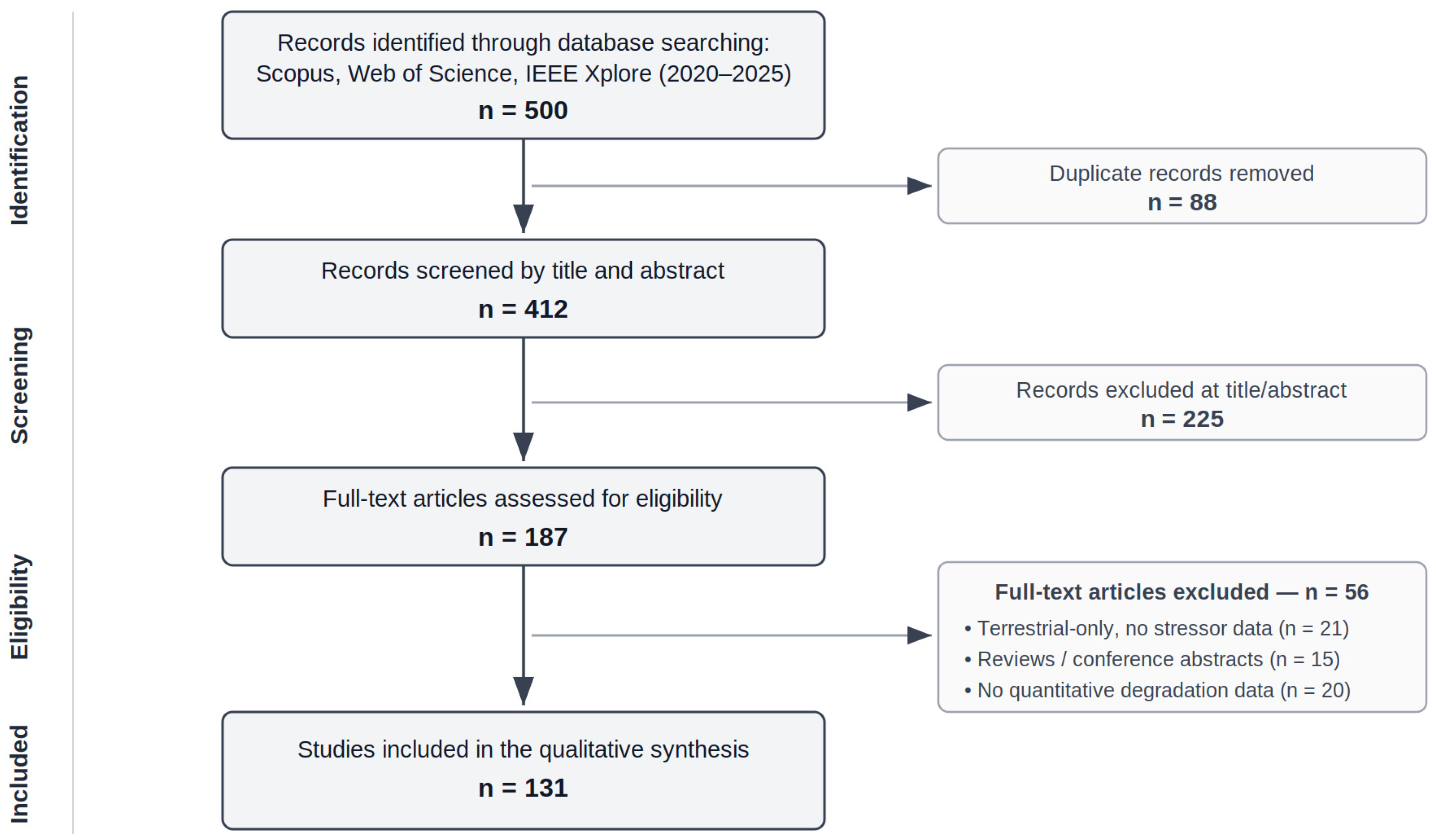
This review was conducted in accordance with the principles of systematic literature analysis. A comprehensive search of the Scopus (Elsevier, Amsterdam, the Netherlands), Web of Science (WoS, previously known as Web of Knowledge, Clarivate, Philadelphia, PA, USA), and IEEE Xplore (Institute of Electrical and Electronics Engineers and Institution of Engineering and Technology, New York City, NY, USA) databases was performed using the following query strings: (“perovskite solar cell”) AND (“space” OR “aerospace” OR “radiation” OR “extreme environment”), (“perovskite stability”) AND (“vacuum” OR “thermal cycling” OR “AM0”), and (“machine learning” OR “LSTM”) AND (“perovskite” OR “photovoltaic degradation”). The three query families were executed independently in each database. Following retrieval, all records were pooled and de-duplicated, resulting in 412 unique records for title and abstract screening after the removal of 88 duplicate records. Initial screening excluded 225 records that did not meet the scope of the review, leaving 187 articles for full-text assessment. During the full-text evaluation, 56 studies were excluded for the following reasons: exclusive focus on terrestrial applications without exposure to relevant space or harsh-environment stressors (n = 21); review papers or conference abstracts rather than original research articles (n = 15); and lack of quantitative performance or degradation data under vacuum, AM0/UV exposure, irradiation, or thermal cycling conditions (n = 20). Consequently, 131 studies satisfied all eligibility criteria and were included in the qualitative synthesis. The complete study-selection workflow is presented in Figure 1.
The selected literature is organized thematically across the following sections: (i) fundamental degradation mechanisms under vacuum, UV, and thermal stress; (ii) absorber and transport-layer engineering; (iii) optical optimization and structural protection; (iv) scalable and vacuum deposition methods; and (v) AI-assisted predictive design and lifetime forecasting.
It is acknowledged that the present review has several inherent limitations. First, the search was restricted to peer-reviewed journal articles in English; conference proceedings and preprints were excluded, which may have introduced a recency bias toward established results. Second, the focus on non-terrestrial stressors means that some advanced passivation and encapsulation strategies developed exclusively for terrestrial applications, but potentially transferable to space, may be underrepresented. Third, the quantitative performance benchmarks cited throughout this review (PCE, T80 lifetime, outgassing rates) are predominantly drawn from accelerated laboratory aging tests rather than from verified in-orbit data, which remain scarce. These limitations define the boundaries of the conclusions drawn and simultaneously highlight the most critical directions for future experimental work.
To keep this distinction traceable, we indicate, in every comparative table and at the principal stability and radiation-tolerance claims, whether the supporting evidence is experimental (terrestrial AM1.5G or accelerated aging) or computational (first-principles/device simulation). No value reported in this review derives from verified in-orbit measurement; genuine flight data remain scarce and are identified throughout as the field’s central outstanding need.

3. Fundamental Mechanisms of Degradation Under Extreme Conditions

Operation of photovoltaic devices in harsh environments (outer space, stratosphere, and highly insolated areas) uncompromisingly exposes the fundamental thermodynamic instability of the organic components underlying classical hybrid perovskites [33]. The formation energy of structures such as MAPbI3 is relatively low, making them extremely vulnerable to external stressors. Exposure to high vacuum combined with severe thermal stress (thermal cycling) [34] provokes the rupture of weak hydrogen bonds within the cuboctahedral voids of the lattice. This inevitably triggers the desorption of the volatile organic cation methylammonium (MA), which leaves the structure in the form of gaseous methylamine and hydrogen iodide [35]. As a result, a phase transition occurs: the photoactive “black” perovskite phase collapses to form a hexagonal, optically inactive, and wide-bandgap insulator, lead iodide (PbI2) [36,37,38,39,40,41]. Without the use of molecular encapsulation barrier layers (such as DPPS), this process can completely stop charge generation in the device [42].
Even with sealing (or under pre-launch above-ground storage conditions), residual moisture and oxygen act as powerful degradation catalysts. Water molecules hydrate the perovskite lattice, radically reducing the activation energy for halide ion migration. This ion migration, under the influence of an internal electric field, not only causes pronounced hysteresis in the current-voltage characteristics but also leads to irreversible corrosion of the metal electrodes (formation of AgI or AuI). Suppressing these processes requires not just chemical additives, but macroscopic architectural solutions: for example, switching to fully coated ITO substrates (“island design”), which physically eliminates vulnerable microgaps through which moisture penetrates [43,44].
A separate and extremely dangerous challenge for the space spectrum (AM0) is high-intensity UV radiation. Exposure to UV radiation triggers a mechanism of photoinduced phase segregation of halides. In perovskites with mixed halides (e.g., I/Br), constant insolation causes the homogeneous alloy to disintegrate into iodine-rich and bromine-rich domains. The resulting iodine-rich domains have a narrowed band gap and begin to act as recombinant traps (the “funnel” effect), which leads to a substantial drop in open-circuit voltage (Voc) [45,46]. Together with the inherent toxicity risks of water-soluble lead (which is critical for terrestrial applications), these factors force a complete revision of the absorber chemical composition.
Attempts to replace lead with its closest environmentally friendly analogue, tin (Sn), have encountered a serious quantum-chemical barrier. In lead-free tin-based semiconductor cells, the critical problem is the extremely rapid oxidation of the Sn2+ ion to Sn4+. Since the 5 s electrons of tin have a higher energy than those of lead, even trace amounts of oxygen (or internal redox reactions) initiate the formation of tin vacancies. This process causes powerful p-type self-doping of the film. The increased hole concentration shifts the Fermi level, disrupts the alignment of energy bands with the transport layers, and generates substantial dark leakage currents, reducing the cell efficiency to a minimum [47,48,49].
To overcome the described complex degradation barriers, modern materials science is implementing a radical and scientifically substantiated transition from classical single-cation systems to architecturally and chemically complex structures. This transition is unfolding in three strategic directions: entropic stabilization of hybrid phases, complete elimination of organic components, and computational design of alternative lead-free lattices.
The first step toward improving stability was compositional engineering aimed at artificially increasing the configurational entropy of the crystallized film [50]. Mixing various cations in the A position (such as cesium, formamidinium, and methylammonium—Cs/FA/MA) and halides (iodine and bromine) allows for a reduction in the free energy of the photoactive “black” phase of perovskite. This multi-cationic architecture effectively suppresses the spontaneous transition to the non-photoactive yellow phase under thermal stress and minimizes the possibility of photoinduced halide segregation under UV irradiation [45].
However, for deep-space applications, the presence of any volatile organic cations (FA or MA) remains a critical risk factor due to vacuum desorption. Therefore, the most reliable development vector is the introduction of fully inorganic perovskites, such as CsPbI3 or mixed-halide CsPbI2Br [51,52]. The complete elimination of organics imparts outstanding thermal rigidity to the structure. The main challenge here remains the stabilization of the highly symmetric cubic α-phase at low temperatures, which is currently being successfully addressed through precision doping with elements with small ionic radii and the use of vacuum deposition methods.
At the same time, to address the toxicity of lead and the instability of Sn2+, an intensive search is underway for thermodynamically stable lead-free alternatives. Among lead-free double perovskite alternatives, Cs2SnI6 stands out due to its Sn4+ valence state, which renders it immune to the p-type self-doping that plagues conventional Sn2+ systems [53]; a detailed analysis is provided in Section 4.
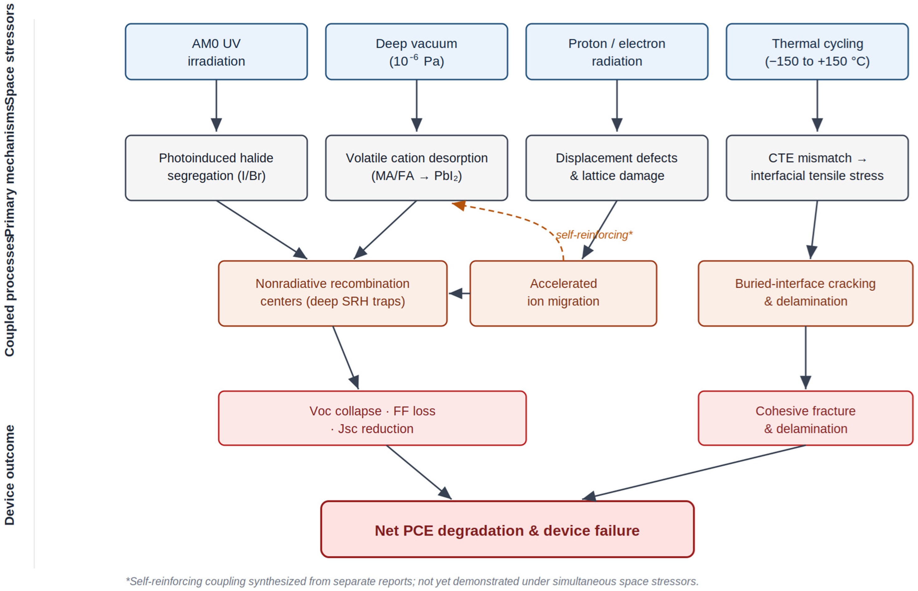
Taken together, the degradation mechanisms acting on PSCs in extreme environments form a coupled, hierarchical threat matrix. At the molecular level, vacuum-induced desorption of organic cations (MA, FA) irreversibly destroys the photoactive phase. At the electronic level, UV-triggered halide segregation and Sn2+ oxidation generate nonradiative recombination centers that collapse the open-circuit voltage. At the macroscopic level, CTE mismatch at buried interfaces under repeated thermal cycling (−150 °C to +150 °C) accumulates tensile stress that ultimately leads to cohesive fracture and delamination.
Critically, these mechanisms are unlikely to act in isolation. The individual couplings—radiation-induced defect generation, defect-accelerated ion migration, and migration-assisted lowering of the desorption barrier—are each documented in separate studies, but their concerted operation as a single self-reinforcing cascade under simultaneous space stressors has not, to our knowledge, been demonstrated experimentally. We therefore present this cascade as a mechanistic synthesis of separately reported effects rather than a directly observed phenomenon; its verification under combined AM0, vacuum, irradiation, and thermal-cycling loading is a priority for future work.
The full stressor-to-failure pathway is summarized schematically in Figure 2.
This mechanistic understanding directly defines the engineering requirements addressed in the following sections, namely, the complete elimination of volatile organic components (Section 4), precision control of film crystallinity (Section 5), and chemical stabilization of buried interfaces (Section 6).

4. Absorber Engineering: Lead-Free and Inorganic Systems

As established in Section 3, vacuum-induced desorption of volatile organic cations is the primary failure mode of hybrid perovskites under space conditions. The most established route to eliminating this risk is the transition to fully inorganic cesium–lead systems, specifically CsPbI3 and mixed-halide CsPbI2Br [51,54,55], whose complete absence of organic components imparts outstanding thermal rigidity. However, the implementation of these materials presents a serious thermodynamic challenge: polymorphism. The cubic (photoactive “black”) α phase of CsPbI3, optimal for photovoltaics, is thermodynamically stable only at high temperatures (above 320 °C). When cooled to room temperature or exposed to the slightest traces of moisture, this structure undergoes a spontaneous phase transition, collapsing into the orthorhombic (non-photoactive “yellow”) δ phase, characterized by a wide band gap and a complete absence of photoelectric properties. Precision crystallization engineering is used to fix the metastable α phase: the use of additives that control nucleation (for example, sodium 4-amino-2-hydroxybenzoate), the introduction of quantum dots as crystallization centers, and the method of generating seed crystals. These approaches create a strong steric hindrance to lattice rearrangement, “freezing” the desired phase and ensuring the maintenance of high efficiency even after thousands of hours of operation [51,54,55].
In addition to thermal instability, a pressing problem for terrestrial and aerospace photovoltaics is the toxicity of lead and its tendency to form deep defects under ionizing radiation. Lead-free double perovskites demonstrate significant scientific and engineering potential in solving these problems. A special place among them is occupied by vacancy-ordered double perovskites (defect-ordered, elpasolite-related structures), such as cesium hexaiodostannate (Cs2SnI6). The main breakthrough of this architecture lies in the valence state of the metal: tin here is initially stabilized in the highest oxidation state (Sn4+) [53]. This quantum-chemical elegance completely eliminates the main cause of degradation of traditional tin perovskites, the thermodynamic tendency toward oxidation Sn2+ → Sn4+. As a consequence, Cs2SnI6 is not susceptible to avalanche-like p-type self-doping, exhibits high defect tolerance, excellent charge carrier mobility, and substantial resistance to oxygen, moisture, and thermal stress [53]. This formal oxidation-state advantage does not, by itself, translate into device performance. In practice, Cs2SnI6 remains constrained by an indirect band gap that limits the attainable open-circuit voltage, by experimentally demonstrated efficiencies that are still well below those of lead-halide references, and by a defect chemistry—dominated by tin and iodine vacancies—that can impose intrinsic carrier-density and recombination penalties. Reported film quality and reproducibility are likewise sensitive to processing atmosphere and iodine stoichiometry. The Sn4+ valence state thus eliminates one major degradation pathway without resolving the broader optoelectronic and fabrication challenges that currently keep this material below the performance threshold required for practical aerospace deployment.
In parallel, a large-scale computational and experimental search is underway for alternative stable phases, where toxic lead is replaced by elements with similar optoelectronic properties. Structures based on germanium (Ge) and bismuth (Bi) are highly promising; when integrated with properly selected electron transport layers (e.g., TiO2 or graphene interfaces), they are capable of forming defect-free transitions with optimal energy band alignment [56,57,58,59].
However, chalcogenide perovskites, such as CaHfS3 and CaZrS3 [60], are emerging as particularly promising candidates for operation under conditions of high-energy cosmic radiation (HEER) [61]. Their fundamental difference lies in the replacement of halogens (iodine, bromine, chlorine) with chalcogens (sulfur, selenium). This transition alters the very nature of chemical bonds: relatively weak metal–halogen ionic bonds are replaced by exceptionally strong covalent–ionic metal–chalcogen bonds. These materials retain the perovskite structure (orthorhombic Pnma syngony) but possess large lattice binding energy. They are insoluble in water, do not degrade under intense UV radiation, are not subject to ion migration in a vacuum, and have an ideal band gap (1.7–2.38 eV) for tandem devices. This physical and chemical “rigidity” makes chalcogenide perovskites a promising route toward radiation-resistant and long-lasting energy platforms for deep space, although this potential remains to be demonstrated experimentally.
It must be emphasized that these conclusions rest almost entirely on first-principles and device simulations. Experimentally, chalcogenide-perovskite thin-film devices remain at an early stage: reported thin-film PCEs are below 5%, high-quality films typically require sulfurization at temperatures incompatible with current perovskite stacks, and no scalable, low-temperature deposition route has yet been demonstrated. The radiation-hardness and vacuum-stability advantages, while physically well-motivated by the strong metal–chalcogen bonding, therefore remain projected rather than verified under AM0 or in-orbit conditions.
Table 1 provides a comparative summary of the key absorber candidates discussed in this section, drawing on experimental and computational results from the reviewed literature. The data reveal a fundamental stability–efficiency trade-off that constitutes the central materials challenge of the field. MAPbI3, despite holding the efficiency record (PCE > 26%), exhibits substantial vacuum instability due to methylammonium desorption [33,35,42] and is effectively disqualified for space deployment. All-inorganic CsPbI2Br achieves a reasonable balance of efficiency (~18%) and thermal rigidity through suppression of the δ-phase transition [51,54,55], but retains lead and requires strict nucleation engineering for phase stabilization. Cs2SnI6 eliminates the Sn2+ oxidation pathway, and its Sn4+ valence state is thermodynamically terminal and shows high defect tolerance [53], but its indirect bandgap (~1.48 eV) intrinsically limits achievable Voc. Germanium- and bismuth-based alternatives offer environmental advantages but suffer from oxidation instability and low efficiencies [57]. Chalcogenide perovskites CaHfS3 and CaZrS3 represent the most stability-favorable candidates surveyed here [60,61,62]: their strong covalent metal–chalcogen bonds render them insoluble, UV-resistant, and immune to ion migration. This performance gap defines the boundary conditions for the crystallization engineering strategies discussed in the following section.
Throughout Table 1, the PCE values for MAPbI3, CsPbI2Br, Cs2SnI6, CsGeI3, and the Bi-based absorber are best-reported experimental laboratory results, whereas the entries for CaHfS3 and CaZrS3 are projected from simulation, as marked. The vacuum-stability and radiation-tolerance columns are qualitative assessments (see criteria above) that blend experimental and computational evidence and should not be read as measured space-qualification data.

5. Crystallization Control and Solvent Engineering

Even when using thermodynamically stable inorganic or lead-free compounds, the macroscopic quality of the absorber film remains a fundamental bottleneck in the technology. The optoelectronic perfection of the device critically depends on the crystallization kinetics. Traditional solution deposition methods often lead to uncontrolled and ultrafast supersaturation, leading to the formation of small grains, through micropores (pinholes), and a substantial density of defects at domain boundaries. These defects act as centers for nonradiative Shockley–Read–Hall recombination and pathways for accelerated ion migration.
To control the thermodynamics of film growth, a spatial–chemical modulation architecture was developed, specifically a dual modification strategy. The use of inorganic quantum dots (e.g., CsPbBr3) in the bulk precursor and surface treatment with agents (such as PEAI) create a synergistic effect. Quantum dots act as centers of heterogeneous nucleation, artificially lowering the energy barrier to crystal formation and directing the growth of large, strictly oriented grains. Surface agents, in turn, passivate undercoordinated vacancies at the interface with the transport layer and impart hydrophobicity to the film, radically reducing the density of interfacial traps [64]. Finer molecular control is achieved by introducing protic ionic liquids and bifunctional additives. The addition of ionic liquids (such as methylammonium acetate MAAc or EMIMTFA) implements a two-site regulation strategy: their anions form strong coordination bonds (according to Lewis) with Pb2+ ions, and the cations are linked via hydrogen bridges with halides. This powerful chemical interaction slows down the reaction between the precursor components, eliminating through pores and suppressing the formation of parasitic phases [65,66]. Formic acid (HCOOH) acts as a regulator of colloidal dynamics: it reduces the size of colloidal particles in solution by 90%, prevents deprotonation of organic cations and blocks iodide oxidation, significantly extending the service life (T80) of the film [67].
Controlling the crystal growth rate directly determines their final size and morphology. The use of volatile solid additives (such as ammonium chloride NH4Cl or methylammonium chloride MACl) leads to the formation of intermediate crystalline phases. These transition structures artificially delay the crystallization of the main perovskite phase, and during subsequent thermal annealing, the volatile components sublimate, leaving behind monolithic ultra-large grains with an ideally smooth surface and minimal internal stress [68,69]. For flexible PSCs and deposition over large areas, the addition of 3-mercaptobenzoic acid (3-MBA) is critical; it dynamically accelerates nucleation but inhibits crystal growth, forming mechanically stable films capable of withstanding thousands of bending cycles [18]. For completely inorganic systems (CsPbX3), sophisticated antisolvent engineering is employed: the use of fluorinated compounds (TFT) induces sharp but uniform supersaturation, generating an ultra-dense, non-porous structure [70].
A separate evolutionary leap in solvent engineering is the transition to environmentally friendly (green) chemistry. Classic PSC production is strictly tied to toxic, teratogenic solvents (DMF, NMP) and antisolvents (chlorobenzene), the use of which is unacceptable on a global commercial scale.
The introduction of environmentally friendly alternatives, such as triethyl phosphate (TEP), allows for the complete elimination of the antisolvent quenching step (a quench-free process). Layer-by-layer deposition of TEP ensures smooth evaporation and uniform crystallization, which is critical for the integration of the technology into industrial roll-to-roll conveyors [71].
Furthermore, the use of cosolvent additives such as acetonitrile (ACN) solves one of the major production problems, assembling elements outside a protective atmosphere. ACN displaces water molecules from the precursor coordination complexes, preventing moisture from destroying the unformed lattice. This innovation enables the synthesis of tricationic perovskites with giant grain sizes (up to 190 nm) directly in ambient air with relative humidity, maintaining high device efficiency and radically reducing capital costs for maintaining ultra-clean gloveboxes [72].
The crystallization and solvent engineering strategies reviewed in this section converge on a common principle: the thermodynamic control of nucleation and growth kinetics is as critical to device performance as the chemical composition of the absorber itself. Molecular additives (ionic liquids, formic acid), volatile crystallization directors (NH4Cl, MACl), and surface-passivating agents (PEAI, 3-MBA) each target a specific stage of film formation, from precursor solution stability through grain boundary passivation, and their synergistic combination enables near-defect-free films even under ambient processing conditions. However, a key limitation of current approaches is their dependence on solution processing, which is incompatible with the solvent-free environment required for aerospace-grade manufacturing. The translation of these crystallographic insights into vacuum co-evaporation and ALD protocols, where nucleation and growth must be controlled through precursor flux and substrate temperature rather than molecular additives, represents a critical and largely unresolved challenge. This manufacturing transition is addressed in Section 8.

6. Modification of Transport Layers and Buried Interfaces

The properties of internal interfaces are now recognized as a primary determinant of both efficiency and operational lifetime in perovskite devices: they govern charge-carrier extraction and recombination, set the energy-level alignment between absorber and transport layers, and control the chemical and mechanical stability of the stack under stress [73]. In the space context, this role is amplified—the same interfaces are simultaneously the dominant locus of nonradiative recombination, the gateway for halide and volatile migration, and the mechanical weak point under thermal cycling. Interface design therefore carries a disproportionate share of the burden in realizing radiation-hardened, vacuum-stable PSCs, and the following discussion treats transport-layer chemistry and buried-interface engineering as one coupled problem rather than as independent layers.
For successful operation of perovskite solar cells in outer space, thermodynamically stabilizing the light-absorbing layer alone is insufficient. The charge-transport layers remain the “Achilles heel” of traditional architectures (both direct n-i-p and inverted p-i-n). Classic high-performance organic hole conductors, such as Spiro-OMeTAD or PTAA, critically depend on the use of hygroscopic dopants, lithium salts (Li-TFSI) and tert-butylpyridine (tBP). Under high vacuum and thermal stress, these dopants undergo intense volatile desorption. Their evaporation not only disrupts hole transport pathways, increasing the cell’s series resistance, but also provokes chemical degradation of the adjacent perovskite. Replacing hygroscopic and unstable organic layers with dopant-free inorganic analogs that do not require doping is a primary requirement for aerospace applications.
In the electron transport layer (ETL), classic mesoporous titanium dioxide (TiO2) often acts as a catalyst for UV-induced perovskite degradation. Therefore, the industry is actively switching to tin dioxide (SnO2)-based structures. Growing thin SnO2 films using plasma-enhanced atomic layer deposition (PEALD) followed by annealing in a reducing atmosphere, as well as using precision-optimized aqueous solutions, enables the generation of oxygen vacancies. These vacancies act as shallow donors, radically increasing the majority carrier concentration and providing excellent electron extraction [74,75,76].
For operation in extreme temperature conditions and under concentrated radiation (up to 10 Sun), a breakthrough solution is the use of barium stannate (BaSnO3). Device simulations indicate an ideal cubic perovskite-like structure, high projected thermal stability (above 400 K), and good band alignment with the absorber, with modeled tolerance under concentrated illumination up to 10 Sun [77]. Furthermore, the formation of heterojunction inorganic bilayers, such as TiO2/SnO2, allows for the synergistic combination of the advantages of two oxides: this architecture physically blocks the through micropores (pinholes) of the base layer, eliminates leakage currents, and forms a powerful energy barrier that blocks the reverse recombination of holes [78].
The hole transport layer (HTL) undergoes an equally radical transformation. Nickel oxide (NiOx), deposited by vacuum methods (magnetron sputtering, ALD), is becoming the standard for inorganic p-type conductivity. To enhance p-type conductivity without the use of volatile organics, structural doping of NiOx with lanthanum (La3+) ions or humidity modulation during synthesis are used, which induces additional dipoles on the surface and reduces the energy barrier for hole extraction [79,80,81]. Two-dimensional MXenes (transition metal carbides and nitrides) exhibit outstanding barrier properties, their metallic conductivity and close-packed layered structure act as an insurmountable shield against halide migration and radiation penetration [82].
To create ultra-low-cost, radiation-hardened, large-area modules, architectures using inert carbon electrodes, which are chemically neutral and not susceptible to corrosion from migrating iodine ions, are being actively explored [83]. Among organic alternatives capable of withstanding harsh conditions, conducting polymers (with tunable packing density) and metal phthalocyanines (e.g., NiPc) stand out. The massive macrocyclic structure of phthalocyanines forms an ultra-rigid surface barrier that physically blocks the release of volatile components from the perovskite, ensuring long-term stability [84,85,86].
The diverse landscape of inorganic transport layer candidates reviewed above reflects a fundamental engineering constraint: no single material simultaneously optimizes charge extraction efficiency, thermal stability above 400 K, resistance to vacuum outgassing, and compatibility with solvent-free deposition. Table 2 provides a structured comparison of the principal candidates across these parameters, drawing directly on the experimental and simulation results cited in this section. The data reveal three key patterns. First, SnO2—particularly when grown by PEALD, emerges as the most mature ETL candidate, combining high electron mobility, controllable oxygen vacancy concentration, and full compatibility with ALD-based manufacturing [74,75,76]. Second, the TiO2/SnO2 bilayer architecture uniquely combines the pinhole-blocking capacity of a dense SnO2 underlayer with the established band alignment of TiO2, at the cost of a more complex two-step deposition process [78]. Third, on the HTL side, La-doped NiOx deposited by vacuum methods represents the current state of the art for dopant-free inorganic hole transport [79,80], while 2D MXenes, despite their exceptional barrier and conductivity properties, lack systematic characterization under sustained proton irradiation and remain at a lower technology readiness level for flight applications [82]. Carbon counter-electrodes and NiPc represent the most chemically inert electrode options for radiation-hardened architectures, though each carries a distinct performance trade-off [83,84,85]. These gaps directly define the experimental priorities for transport-layer qualification under space-simulated conditions.
Several cross-cutting conclusions emerge from Table 2. One disadvantage is the hole transfer layers, which depend on hygroscopic and volatile additives (most notably Spiro-OMeTAD and PTAA doped with Li-TFSI and tert-butylpyridine) since these additives desorb under the combined stress of deep vacuum (10−6 Pa) and thermal cycling and are therefore poorly suited to aerospace tasks. This concern is specific to volatile-doped and solution-processed organic layers rather than to organic chemistry as such: solvent-free, vacuum-deposited molecular conductors such as metal phthalocyanines (e.g., NiPc) can satisfy the vacuum-compatibility criterion, as reflected in Table 2. The severity of the constraint is also mission-dependent: short-duration low-Earth-orbit payloads tolerate out-gassing budgets that long-duration deep-space missions do not, and robust encapsulation can partially mitigate dopant loss, albeit at the cost of added mass and its own out-gassing burden.
Among the remaining inorganic candidates, SnO2 (PEALD) and La-doped NiOx (ALD/sputtering) form the most technically mature ETL/HTL pair, with demonstrated thermal stability above 400 K and full compatibility with solvent-free manufacturing. BaSnO3 offers superior thermal stability and an ideal perovskite-compatible crystal structure, but its deposition scalability requires further development before it can be considered for large-area flight modules. The 2D MXene interlayers represent a high-potential but low-TRL option whose primary outstanding qualification gap is systematic irradiation testing under ECSS-E-ST-10-04 [88] protocols. Closing this gap, through standardized proton beam exposure (1 MeV equivalent, fluence > 1015 p cm−2) followed by electrical and morphological characterization, is identified as a high-priority near-term experimental objective.
A particular focus of modern engineering is on so-called “buried interfaces”, the interfaces between the hard inorganic transport layer and the soft perovskite lattice. Mechanical stress and dangling bonds at this boundary generate deep traps that, in several high-efficiency architectures, have been associated with a dominant fraction of total nonradiative recombination losses; this proportion is device- and architecture-specific rather than universal.
The critical boundary determining both the optoelectronic efficiency and the physical survivability of a perovskite element under extreme conditions is the “buried interface”, the interface between the hard inorganic transport layer and the relatively soft, ionic perovskite crystal lattice. Due to the difference in lattice parameters (lattice mismatch) and the mismatch of the coefficients of thermal expansion (CTE), large tensile mechanical stress accumulates at these interfaces [89]. Furthermore, the break in the lattice periodicity generates a high density of undercoordinated ions (e.g., open Pb2+ centers or halide vacancies), which act as deep traps for charge carriers, triggering nonradiative Shockley–Read–Hall recombination. To address this problem comprehensively, modern interface engineering is abandoning simple physical coatings in favor of precision chemical design of transition zones. The strategy for introducing chemical bridges is to use bidentate molecules (e.g., diammonium salts or Lewis base molecules). These molecules have two reactive ends: one is firmly anchored in oxygen vacancies of the oxide transport layer (e.g., SnO2), and the other is embedded in the perovskite lattice, binding to lead ions. This molecular “cross-linking” not only chemically passivates charged defects but also acts as a nanoscale shock absorber. It is capable of reversible deformation, relieving accumulated tensile stress, which allows structures to withstand thousands of severe thermal cycles and extreme bending without delamination [90,91,92,93,94].
In parallel, the formation of two-dimensional (2D) perovskite layers on top of a classic 3D absorber is being actively used to protect frontal interfaces. The incorporation of bulk organic cations (bulky cations), which are too large to be incorporated into a standard 3D lattice, results in the formation of an ultrathin 2D capping layer. This low-dimensional structure has increased formation energy and hydrophobicity. It acts as a powerful physical and energetic barrier: the 2D layer blocks the release of volatile components from the 3D perovskite into vacuum, halts the migration of iodine ions to the metal electrodes, and heals surface vacancies, dramatically extending the service life of the cell without significantly blocking charge transfer.
A special area of green chemistry has emerged in the use of environmentally friendly cross-linking polymers such as polysuccinimide (PSI) and polyasparagine (PASP). Unlike rigid inorganic passivators, these long-chain polymers are capable of flexibly enveloping perovskite grains. The high density of carbonyl groups (C=O) in the polymer chain ensures strong Lewis acid-base interactions with antisite defects and undercoordinated lead. The polymer matrix not only “draws” excess parasitic PbI2 but also forms an elastic intergranular framework. This framework prevents grain boundary sliding during mechanical vibrations (typical during the launch phase of spacecraft) and maintains the structural integrity of the active layer [95].
Finally, self-assembled monolayers (SAMs) have become a powerful tool for quantum-mechanical interface tuning. SAM molecules consist of an anchoring group (e.g., phosphonic acid), a carbon spacer, and a functional terminal group. When deposited on transparent conductive oxides (ITO/FTO) or a NiOx layer, they form a strictly oriented, close-packed monomolecular layer.
A unique property of SAMs is their ability to generate a powerful tunable surface dipole moment. This dipole can deliberately shift the work function (vacuum level shift) of the adjacent electrode, ensuring perfect cascade energy band alignment between the transport layer and the perovskite valence band. This precise energy band alignment completely eliminates energy barriers to charge extraction, suppresses reverse interfacial recombination, and maximizes the fill factor of the device [96].
The combined interface-engineering toolkit: molecular cross-linkers, 2D/3D passivation, polymer matrices, and SAM band alignment, has delivered PCEs above 25% and retention above 90% after 6000 bending cycles. These benchmarks, however, were obtained under terrestrial or ambient-laboratory conditions (AM1.5G illumination, mechanical flexing, moderate thermal stress). To our knowledge, none of these engineered architectures has yet been characterized under the full space-relevant load set: sustained proton/electron irradiation (>1015 p cm−2), deep vacuum (10−6 Pa), and wide-range thermal cycling (−150 to +150 °C). Closing this verification gap is a prerequisite for flight qualification and remains, at present, almost entirely unaddressed in the published literature [90,97].
Beyond their electronic passivation function, polymer crosslinkers and bidentate interfacial molecules contribute significantly to the mechanical integrity of perovskite device stacks by redistributing local stress and suppressing crack propagation at buried interfaces. Quantitative studies indicate that conventional PSC architectures often exhibit relatively low interfacial fracture energies, typically below 1.5 J m−2 and, for the weakest interfaces, as low as 0.12–0.42 J m−2. The incorporation of multidentate anchoring groups and crosslinked networks increases cohesion, reduces grain-boundary sliding, and limits delamination during repeated deformation. These modifications have enabled flexible PSCs to maintain more than 90% of their initial efficiency after 6000–10,000 bending cycles and to preserve stable performance during approximately 200 thermal cycles. Collectively, these findings demonstrate that advanced interfacial engineering can substantially improve the mechanical reliability of perovskite photovoltaic devices.
These interface solutions must ultimately be integrated with the light-trapping and mechanical protection architectures discussed in Section 7.

7. Optical Optimization and Structural Protection

In space conditions (the AM0 spectrum), solar cells are exposed to unfiltered electromagnetic radiation, characterized by high intensity in both the high-energy ultraviolet (UV) and infrared (IR) ranges. Traditionally, thickening the absorber layer to capture more photons inevitably leads to an increase in the charge transport path, which, in the presence of radiation-induced defects, critically reduces the likelihood of their successful extraction. Therefore, aerospace photovoltaics requires the creation of ultrathin architectures with artificially enhanced absorption (light trapping) and integrated protection against parasitic heating and UV degradation.
Plasmonic nanooptics is a breakthrough tool for achieving superabsorption in thin films. The integration of metal nanoparticles (MNPs), such as gold (Au) or silver (Ag), allows for the excitation of localized surface plasmon resonance (LSPR). When the frequency of incident light coincides with the oscillation frequency of the electron gas on the nanoparticle surface, a substantial near-field enhancement occurs, which is transferred directly to the valence band of the perovskite. Moreover, plasmonic nanoparticles act as subwavelength scatterers, increasing the optical path length of photons inside the absorber [98,99,100].
However, direct contact between the metal and the perovskite or transport layers generates a “hotspot” effect, causing localized thermal overheating and creating powerful nonradiative recombination centers. To isolate these processes, a hybrid plasmonic–dielectric core–shell architecture, such as Au/Al2O3, has been developed. The ultrathin aluminum oxide dielectric shell not only shifts and tunes the plasmonic resonance peak due to its refractive index but also acts as a reliable physical barrier. It prevents parasitic recombination of hot electrons on the gold surface, ensuring photocurrent growth without thermal damage to the lattice [99,101].
In parallel with plasmonics, macroscopic nanostructuring of transport layers is being implemented. The formation of 2D photonic crystals (PhCs) based on arrays of cylindrical TiO2 nanostructures causes strong coupling of optical modes with surface plasmon polaritons (SPPs). This radically enhances light absorption at any incidence angle and polarization, allowing even hole-layer-free (HTL-free) structures to increase absorption efficiency by 16% [102,103].
Antireflective layers (PARLs) based on pyramidal arrays perform a similar function. Forming a composite “pyramid/pore” structure on the front surface or at the interface with the ETL smooths out the refractive index jump. The pyramids induce multiple internal refraction and reabsorption (light trapping), which reduces the reflectivity from 40% to 5% and increases the generated current density by more than 22% in ultrathin geometries [104,105].
To utilize photons whose energy lies outside the perovskite band gap, upconversion nanoparticles (UCNPs) doped with rare earth elements (e.g., erbium) are used. The integration of UCNPs together with carbon quantum dots enables spectrum conversion: they absorb low-energy IR photons and re-emit them in the visible range, which is then effectively absorbed by the perovskite. Quantum dots additionally passivate grain boundaries, suppressing the phonon bottleneck and accelerating electron transport [106,107].
Finally, a critical challenge for the AM0 spectrum is protection from harsh UV radiation, which instantly disrupts organic bonds and activates the photocatalytic properties of oxide transport layers (such as TiO2). Traditional thick polymer filters are unacceptable due to their weight and degradation in vacuum. The solution was the use of UV-blocking metasurfaces.
Thin-film metasurface filters based on precisely calibrated silver nanoparticles form an ultra-narrow resonant absorption peak (e.g., at 403 nm). They act as a selective optical shield: they reliably block destructive ultraviolet light, preventing degradation of the active layer, while transmitting the rest of the visible and IR spectrum with minimal losses (the reduction in useful absorption is no more than 2%). This architectural elegance ensures a radical extension of the service life (T80) of photovoltaic platforms in orbit [108].
Extreme aerospace conditions subject solar panels not only to radiation and temperature but also to large mechanical stress. During the spacecraft’s orbital insertion, the elements experience powerful acoustic shocks, high-frequency vibrations, and overloads. In orbital flight conditions, extreme thermal cycling (temperature fluctuations with changing illumination) induces shear deformations at the interfaces of layers due to mismatched coefficients of thermal expansion (CTE). Since traditional polycrystalline perovskite films and inorganic oxide transport layers (SnO2, NiOx) are highly brittle, these stressors inevitably lead to microcracking, cohesive failure, and delamination of the interfaces. An additional destructive factor is the deep vacuum of space (10−6 Pa), which acts as a powerful pump, drawing volatile components from the crystal lattice (vacuum degassing).
To provide comprehensive protection against these threats, modern engineering is moving beyond simple surface sealing to the concept of internal structural encapsulation and nanoreinforcement. A fundamental breakthrough has been the introduction of cross-linking biopolymers and elastomeric matrices directly into the bulk of the light-absorbing layer.
The use of non-toxic polysaccharides, such as gellan gum, as a rheological additive in scalable blade coating fundamentally changes film mechanics. Polymer molecules disperse along grain boundaries during crystallization, forming a flexible three-dimensional “network-frame.” This network acts as a nanoscale shock absorber that effectively dissipates mechanical stress and prevents crack propagation. As a result, the cohesive fracture energy (Gc) of the perovskite layer increases severalfold, transforming the brittle ceramic into a shock-resistant composite [109].
A similar, but even more complex, function is performed by the introduction of polyvinyl alcohol (PVA) matrices. Long PVA polymer chains, due to the abundance of hydroxyl groups, tightly envelop each individual perovskite grain, creating a “brick-and-mortar” architecture. This polymer capsule performs a triple function: first, it imparts extreme resistance to mechanical bending and impact to the cells; second, it physically blocks the diffusion paths of volatile components into the vacuum; third, it acts as a reliable barrier (trap) for Pb2+ ions, preventing the leakage of toxic lead even in the event of complete physical destruction of the module [110].
One qualification applies uniformly to the polymeric additives introduced in Section 6 and Section 7 (gellan gum, PVA, PSI/PASP, and related matrices): their demonstrated benefits (fracture toughening, lead sequestration, and grain-boundary reinforcement) have been established under terrestrial conditions, while their behavior under space stressors is largely uncharacterized. Organic polymers are, in particular, prone to vacuum outgassing, and spaceflight suitability is conventionally screened against standards such as ASTM E595 (total mass loss < 1.0%, collected volatile condensable material < 0.1%). Comparable outgassing, long-term radiation-stability, and deep-vacuum data for these specific additives are, to our knowledge, not yet available. Their integration into flight-grade devices is therefore contingent on dedicated vacuum- and radiation-compatibility testing.
To combat internal mechanical stress caused by lattice mismatches and thermal expansion coefficients at heterointerfaces, graded buffer layers are used. Unlike abrupt (stepped) transitions between materials, compositionally graded structures (for example, based on variable GaAs1−xNx composition or a smooth transition of transport oxides) create an adaptive buffer zone.
They smoothly distribute thermomechanical stress throughout the entire buffer volume, preventing the concentration of shear forces at a single buried interface. This prevents ultrathin cell layers from rupture and delamination during sharp temperature changes (from −150 °C to +150 °C) in orbit [111]. Finally, for protection against vacuum outgassing and exposure to aggressive environments at the molecular level, a multidimensional (2D/3D) encapsulation strategy is used [112]. Forming a thin layer of 2D perovskite or using massive organic salts (such as methyltriphenylphosphonium iodide—MTPPI) on the surface of a 3D absorber creates a “molecular sealing” effect. Massive cations physically bridge grain boundaries and micropores, blocking the release of methylammonium and iodine molecules into open space, and also preventing the penetration of residual oxygen into the internal layers of the device [113].
A caveat applies across the optical strategies surveyed here. Several—plasmonic core–shell absorbers, photonic-crystal texturing, and upconversion layers—have been validated mainly in simulation (e.g., FDTD) or in terrestrial full devices under AM1.5G, rather than under the AM0 spectrum with concurrent vacuum and particle irradiation. Their projected gains in light harvesting and UV protection should therefore be regarded as promising but largely unverified for space conditions, where the same nanostructures must additionally survive radiation-induced damage and thermal cycling without optical or mechanical degradation.
Plasmonic core–shell nanostructures, 2D photonic crystals, and biopolymer scaffolds collectively enable near-unity photon harvesting in absorbers below 300 nm while transforming brittle perovskite ceramics into composites capable of surviving launch acoustic loads and LEO thermal cycling. A key insight is that optical and mechanical strategies are not independent: polymer matrices and 2D capping layers simultaneously passivate grain boundaries and attenuate UV. These architectures must ultimately be fabricated by solvent-free vacuum processes, addressed in Section 8.

8. Scaling, Vacuum Methods and Tandem Structures

A fundamental barrier to the integration of perovskite photovoltaic technologies into the aerospace industry and global energy is the problem of scalability. Laboratory efficiency records (over 26%) have traditionally been achieved using liquid centrifugation (spin-coating). However, this method is fundamentally incompatible with industrial production: it results in the loss of up to 90% of the precursors, is limited to small areas (fractions of a square centimeter), and, most critically for space applications, leaves microscopic traces of toxic solvents (DMF, DMSO) within the film. Under high vacuum conditions, these residual solvents undergo intense outgassing, disrupting the perovskite crystal lattice from within and causing substantial delamination of the elements. The future of high-reliability PSC production for extreme environments is inextricably linked to the transition to completely “dry” vacuum technologies. Vacuum deposition guarantees the formation of ultra-pure films without the use of solvents, ensuring perfect coating conformality and precise stoichiometry control.
Among the advanced vacuum approaches, pulsed laser deposition (PLD) stands out. In this method, a high-energy laser pulse evaporates a solid target (containing perovskite or inorganic transport layer components), forming a plasma plume that is deposited onto a substrate. The uniqueness of PLD lies in its congruent (stoichiometric) material transfer: the chemical composition of the target is reproduced with 100% accuracy in the thin film [114]. This enables the construction of multilayer (tandem) architectures without the risk of the liquid solvent of the top layer washing away or damaging the underlying layers.
For the formation of precision barrier and transport layers (such as SnO2, NiOx, or Al2O3), atomic layer deposition (ALD) is becoming the standard. The process is based on self-limiting surface reactions in the gas phase, enabling the growth of layers with single-atom precision (~1 nm in 10 cycles). ALD provides perfect conformal (defect-free) coatings even on rough or textured surfaces (e.g., on arrays of nanowires or pyramids), reliably sealing micropores and blocking leakage currents [115]. The development of spatial ALD (S-ALD) solves the problem of low process speed, paving the way for its integration into industrial production lines.
Equally effective for synthesizing the absorber itself are co-evaporation and chemical vapor deposition (CVD) methods. Strict control of precursor vapor pressure (e.g., sublimation of cesium and lead halides) and substrate temperature allows for the thermodynamics of adsorption and recrystallization to be controlled. This forms highly oriented crystalline domains without the residual stress characteristic of rapidly drying liquid films [116,117].
While vacuum methods remain the preferred route for spacecraft and tandems, mass production of inexpensive PSCs for terrestrial applications requires a transition to continuous roll-to-roll (R2R) printing technologies. Slot-die coating is currently recognized as the most cost-effective technology for scaling. In this method, perovskite ink is continuously extruded through a narrow slit (matrix) onto a moving flexible substrate. Forming a stable liquid meniscus requires delicate rheological engineering of precursor solutions: fine-tuning of viscosity, surface tension, and drying kinetics. The use of environmentally friendly solvent systems and polymer rheological additives enables the formation of uniform, dense films on modules with an area of over 300 cm2 [19,118].
High-speed inkjet printing is being actively implemented to create elements with complex geometries and integrate PSCs into flexible electronics. This contactless method enables the deposition of picoliter droplets of precursors with micron precision, forming specified patterns without the use of photolithography or chemical etching. Optimizing the surface energy of the droplets prevents the “coffee ring” effect and ensures uniform crystallization [119,120,121].
However, the main technological barrier in roll-to-roll production remains the thermal annealing process of the films, which takes tens of minutes in traditional ovens, slowing down the conveyor belt and damaging inexpensive polymer substrates (such as PET or PEN). Photonic curing technology has emerged as a solution. Using high-intensity millisecond pulses from broad-spectrum xenon lamps, the perovskite layer (or NiOx/SnO2 nanoparticle layer) can be instantly heated and sintered to temperatures of hundreds of degrees, without melting the underlying plastic substrate. This method dramatically reduces fabrication time from hours to milliseconds by inducing grain coarsening through localized thermal shock and paving the way for gigawatt-scale commercial production of flexible perovskite modules [122].
Table 3 provides a comparative assessment of the deposition methods reviewed in this section across the key parameters relevant to aerospace manufacturing. The data illustrate the fundamental incompatibility of solution-based methods with space-grade film purity requirements and confirm that vacuum deposition routes, despite higher capital cost—are the only physically viable path for PSC integration into spacecraft power systems.
The fundamental thermodynamic limitation on the efficiency of any single-junction solar cell is the Shockley–Queisser limit. The majority of energy losses in classical photovoltaics are due to two factors: the inability to absorb photons with energies below the band gap (Eg) and large thermalization losses when high-energy photons (UV and short-wavelength visible light) generate “hot” charge carriers, whose excess energy is instantly dissipated as heat (phonons) in the crystal lattice.
To circumvent this limit and radically reduce thermalization losses, the concept of multi-junction (tandem) architectures is used. In such systems, the wide-bandgap (WBG) upper subelement (usually perovskite with Eg ≈ 1.6–1.8 eV) effectively absorbs the high-energy part of the spectrum, generating a high voltage, and the part of the spectrum that is transparent to near-infrared (NIR) radiation passes through and is absorbed by the narrow-bandgap (NBG) lower subelement (Eg ≈ 1.0–1.2 eV).
Technologically, tandems are implemented in two basic configurations:
  • Four-terminal (4T) mechanically stacked tandems: Subelements are fabricated separately and optically coupled to each other. This eliminates the need for strict current matching, but requires the development of transparent and optically neutral intermediate electrodes. Optimization of 4T structures requires the implementation of ultrathin metal meshes, buffer-coated silver nanowire (AgNW) layers, and composite structures (DMDs) that minimize parasitic light absorption in transparent contacts [123];
  • Two-terminal (2T) monolithic tandems: The upper element is grown directly on the lower element via a recombination layer (or tunnel junction). This architecture is more technologically advanced and cheaper to assemble, but requires ideal optical and electrical balance (current matching), since the total current of the entire device is limited by the subelement with the lowest current.
A classic solution is the creation of perovskite/silicon tandems (c-Si). To minimize optical loss (reflection) at the interfaces of such monolithic systems, multilayer antireflection coatings (ARCs) are actively used. The use of a HLIS design (alternating thin layers of materials with high and low refractive indices, such as MgF2/ZnS or Al2O3) allows for the refractive index difference at the interfaces to be compensated, minimizing parasitic reflection and increasing the short-circuit current (Jsc) of the tandem [124].
However, heavy and hard silicon is not always suitable for aerospace applications (where specific power (W/g) is important). Therefore, alternative technologies for the bottom subcells are coming to the fore:
  • III-V nanowire arrays: Instead of expensive planar gallium arsenide or indium phosphide (InP) wafers, the bottom subcell is formed as an array of vertical nanowires. This nanoarchitecture radically reduces the reflectivity (acting as an optical trap) and allows for optical decoupling of the subcells, maximizing photon capture with minimal consumption of expensive III-V materials [125];
  • Organic semiconductors (PO-TSC): Creation of all-film, flexible, and ultralight perovskite/organic tandems. The main breakthrough here was the development of new narrow-gap non-fullerene acceptors (NFAs), capable of efficiently absorbing radiation in the deep near-IR range (>1000 nm), compensating for the current deficit of the organic bottom subcell [126].
The creation of a wide-bandgap perovskite (Eg > 1.7 eV) for the top cell requires an increased bromine content in the I/Br alloy. Under intense radiation conditions, this provokes halide segregation (photoinduced phase separation into iodine- and bromine-rich domains). This process is mitigated by fine-tuning the composition (mixing Cs/FA/MA cations) and the mandatory use of self-assembled monolayers (SAMs) for surface passivation, preventing charge accumulation at the interfaces [50].
Finally, a critical issue for operating tandem PSCs in extreme environments (especially in orbit) is the temperature matching of the subcells. When exposed to the AM0 spectrum, the panels inevitably heat up. Simulations of thermodynamic dependencies (SCAPS) show a nonlinear degradation of the operating parameters. Up to 55 °C, the perovskite subcell exhibits outstanding stability (the PCE temperature decay coefficient is only −0.25% K−1), outperforming silicon.
However, when heated above a critical threshold of 55 °C, thermal activation of deep defects in the perovskite is triggered, and its temperature coefficient drops sharply to −0.67% K−1. Since silicon or organic cells react differently to heating, a substantial current mismatch occurs. In a monolithic 2T architecture, this leads to the overheated perovskite top layer physically “choking” the current of the entire tandem. Accurately accounting for this nonlinear temperature dynamics and the design of optically transparent radiators (or graded thermal buffers) is an requirement in the development of multijunction architectures for aerospace missions [127].
For aerospace applications, vacuum deposition (ALD, PLD, co-evaporation) is the only manufacturing route physically compatible with the required film purity and solvent-free composition; for terrestrial large-area production, slot-die coating accelerated by photonic curing offers the viable path to gigawatt-scale output. The nonlinear thermal response of perovskite subcells above 55 °C in monolithic 2T tandems imposes a system-level constraint requiring passive thermal management beyond cell-level optimization. These boundary conditions define the operational envelope within which AI-assisted design, discussed in Section 9, must function.

9. AI Forecasting and Computational Design

The rapid expansion of the perovskite compositional space (multi-cation mixtures, binary and chalcogenide structures) makes the traditional trial and error (Edisonian approach) physically impossible and economically impractical. To accelerate the commercialization and development of radiation-hardened panels for space applications, modern materials science is making a fundamental shift to the inverse materials design paradigm using artificial intelligence (AI) and machine learning (ML) algorithms.
During the materials screening stage, ensemble machine learning algorithms such as random forest and gradient boosting are used to predict the thermodynamic stability of new crystalline structures (including ABO3-type perovskites and elpasolites). Using fundamental descriptors (ionic radii, electronegativity, octahedral factor), these models calculate the lattice formation energy with high accuracy and predict the phase stability of the alloy even before its physical synthesis in the laboratory [128,129,130]. This allows for the immediate elimination of thermodynamically unstable compositions and the focus of resources only on materials capable of withstanding the extreme temperature changes in space.
Once a stable absorber has been selected, device engineering becomes a key consideration. A critical issue when the energy levels of the perovskite and inorganic transport layers misalign is the formation of so-called S-shaped kinks in the current-voltage (I-V) characteristic.
This parasitic effect arises from charge accumulation at interfaces and the formation of extraction barriers, which dramatically reduces the cell’s fill factor. To address this issue, 3D finite element modeling (FEM) and circuit simulation (using optimization algorithms such as the firefly algorithm) are used. Simulations in environments such as SCAPS-1D allow for the precise calculation of the optimal transport layer thickness and gradient doping profile, eliminating S-shaped kinks through ideal energy band alignment [131,132,133]. A comparative analysis of neural network architectures shows that the transition from simple to more complex models (by adding buried layers) in combination with regularization and batch normalization methods significantly increases both the stability of the training process and the accuracy of predictions, enhancing the model’s ability to generalize.
Table 4 summarizes the AI and machine learning architectures reviewed in this section. The data reveal a clear stratification: ensemble methods (random forest, gradient boosting) are mature tools for thermodynamic stability screening but cannot capture temporal degradation dynamics; LSTM networks are the leading architecture for time-series SOH prediction but are fundamentally limited by the quality of training data; and XAI methods (SHAP) currently function as post hoc interpretation tools rather than standalone design drivers. The transition from synthetic to empirical training datasets, discussed in the following paragraphs, is the prerequisite for all three tiers to reach their operational potential.
The implementation of deep learning (DL) algorithms for predictive stability assessment and SOH prediction is of particular and critical importance for aerospace photovoltaics. Traditional degradation assessment methods (such as ISOS aging protocols) rely on lengthy and resource-intensive physical tests in climate chambers. To overcome this barrier, modern science is turning to predictive artificial intelligence models.
In practice, the input feature set for data-driven SOH models comprises the standard photovoltaic descriptors extracted from periodic I–V sweeps—PCE, open-circuit voltage (Voc), short-circuit current density (Jsc), and fill factor (FF)—augmented with the environmental and stress variables that drive degradation: device temperature, cumulative radiation dose or particle fluence, thermal-cycle count, illumination spectrum and intensity, and, where available, electrochemical impedance spectra that separate interfacial from bulk contributions. The temporal evolution of these quantities constitutes the sequence upon which recurrent or attention-based models are trained. A fundamental limitation must, however, be restated: models trained on laboratory accelerated-aging data encode single-stressor, idealized degradation and cannot be assumed to generalize to the coupled AM0/vacuum/irradiation/thermal-cycling environment of orbit (see Table 5).
Analyzing time series data describing cell efficiency degradation under constant thermal and radiation stress requires specialized architectures. Research convincingly shows that long short-term memory (LSTM) neural networks have been the most frequently adopted architecture in the available studies [31,32]. Thanks to a complex system of internal gates (forget gate, input gate, and output gate), these networks overcome the vanishing gradient problem inherent in standard recurrent networks. The reviewed studies [31,32] provide compelling evidence that LSTM networks effectively capture latent temporal dependencies in PSC degradation data and yield predictions of sufficient accuracy to serve as a methodological baseline for SOH monitoring. However, it must be noted that these results were obtained predominantly on synthetic or short-duration experimental datasets, which limits the generalizability of the findings to real orbital operating conditions.
LSTM’s central place in the present review reflects the structure of the available literature [31,32], in which it is the architecture most often applied to PSC degradation series, rather than a demonstrated superiority over competing approaches. Several alternatives are, in principle, equally or better suited to the problem: gated recurrent units (GRUs) offer comparable temporal modeling at lower parameter cost; temporal convolutional networks and attention-based (Transformer) models capture long-range dependencies without the sequential bottleneck of recurrence; and physics-informed neural networks and Gaussian-process regression embed degradation-kinetics priors that can improve extrapolation from sparse data. Because the published PSC degradation datasets are still small, short in duration, and predominantly synthetic, the current evidence base is insufficient to support strong claims about the superiority, or the eventual aerospace reliability, of any single architecture, LSTM included. We therefore frame LSTM as a well-motivated methodological baseline rather than an established optimum, and identify systematic benchmarking against the alternatives above, on standardized empirical datasets, as a necessary next step.
A fundamental aspect of the successful application of DL is the architectural tuning of the model. A comparative analysis between simple and complex predictive models demonstrated that deliberately increasing model complexity, by adding additional buried layers and applying advanced regularization methods, dramatically improves both predictive accuracy and the network’s ability to generalize to new, unknown degradation regimes. In particular, integrating a dropout layer to prevent overfitting and applying batch normalization are critical for improving the stability and training speed of the neural network when working with noisy I–V data.
Throughout these computational studies, key design parameters directly affecting the overall efficiency of PSCs were identified. Visualization and in-depth analysis of these parameters provided critical insights into their physical role and their impact on degradation processes. This offers valuable guidance for future PSC architecture optimizations. Identifying these critical design parameters provides engineers with actionable insights, guiding targeted optimization efforts and minimizing time spent on laboratory material selection.
As deep learning architectures become more complex, the “black box” problem arises: neural networks produce highly accurate predictions but obscure the underlying logic behind their decision-making. To overcome this barrier, explainable AI (XAI) methods, such as SHAP analysis (SHapley Additive ExPlanations), are being actively implemented in aerospace materials science. Deep visualization and interpretation of key design parameters, such as transport layer thickness, interfacial trap density, ion migration activation energy, and doping level, allow AI to extract fundamental physical insights. This analytical process transforms raw data sets into actionable insights. Understanding the contribution of each parameter to the overall performance of a solar cell enables targeted rather than blind optimization, allowing engineers to focus resources only on those architectural components that critically impact cell survivability.
The transformative potential of the ML/DL pipeline described above is currently constrained by a single critical bottleneck: the near-total reliance on synthetic training datasets. The vast majority of published models, whether ensemble methods for stability screening, DNNs for PCE prediction, or LSTM networks for SOH monitoring, are trained on data generated by SCAPS-1D or similar simulation environments. While synthetic datasets enable rapid initial screening, they encode the idealized physics of the simulation and systematically fail to capture stochastic real-world phenomena: thermally induced microcracking, spatially inhomogeneous vacuum degassing, and the complex corrosion kinetics of metal electrodes under prolonged proton bombardment. LSTM networks trained on such data produce SOH predictions accurate within the simulation framework but exhibiting poor generalizability to real orbital operating conditions.
Bridging this gap requires a coordinated effort to generate standardized, publicly accessible empirical datasets from: (i) ground-based space-simulation chambers operating under ECSS protocols; (ii) high-throughput screening platforms capable of aging hundreds of minimodules in parallel under combined vacuum, UV, and particle irradiation; and (iii) real-time telemetry from photovoltaic payloads aboard CubeSat missions. Only when LSTM and DL models are retrained on such empirical data will AI-based SOH prediction achieve the reliability required for autonomous energy management in deep-space missions. The SHAP-based explainability tools reviewed above further reinforce this need: their physical interpretations are only as trustworthy as the data upon which the underlying models were optimized.
The magnitude of the gap can be stated plainly: of the published data-driven PSC models surveyed here, effectively all are trained on synthetic or terrestrial accelerated-aging data, and none has been validated against real orbital telemetry. Table 5 contrasts the available data tiers against the requirements for flight-qualified state-of-health prediction.

10. Conclusions and Prospects

Successful adaptation of PSCs to the harsh conditions of outer space and extreme terrestrial environments cannot be achieved through incremental improvements to classical architectures. Solving this large challenge requires the synergy of fundamental materials science, nanophotonics, advanced precision manufacturing methods, and artificial intelligence algorithms. As an exhaustive analysis of the current literature has shown, ensuring the survivability of photovoltaic platforms beyond the Earth’s atmosphere necessitates a complete conceptual revision of the cell structure at every level.
The fundamental answer to the challenges of thermal desorption in a vacuum and radiation degradation under the influence of the AM0 spectrum is an unconditional transition to thermodynamically rigid systems. The combination of completely inorganic absorbers (such as the α phase CsPbX3, double lead-free perovskites Cs2SnI6 and chalcogenide structures) with inorganic charge-transport layers (SnO2, NiOx, BaSnO3) forms the radiation-hard core of the device. The integration of cross-linking polymer frameworks and elastomeric matrices into this volume radically increases the cohesive strength (fracture energy) of brittle ceramics, allowing the elements to withstand large acoustic shocks and high-frequency vibrations during the launch stage of launch vehicles [97]. In parallel, precision molecular passivation of buried interfaces using self-assembled monolayers (SAMs) and bidentate bridges provides not only cascaded alignment of energy bands but also effective damping of shear thermomechanical stresses.
Scaling these complex multidimensional architectures necessitates abandoning liquid centrifugation in favor of “dry” vacuum deposition methods (ALD, PLD, coevaporation). Only these methods can ensure ideal film conformability without microscopic traces of solvents, eliminating the risk of destructive vacuum degassing.
We invoke Material Flow Cost Accounting (MFCA) [134] because the transition from laboratory devices to deployable hardware is gated as much by manufacturing economics and material efficiency as by intrinsic device physics, and MFCA provides a standardized framework (ISO 14051 [135]) for quantifying and monetizing material, energy, and waste flows across a fabrication chain. MFCA is, however, a process- and supply-chain-level tool: its relevance to aerospace is indirect, operating through the cost and yield of producing complex tandem stacks and through the reduction in expensive precursor losses, rather than through any effect on in-flight device performance or survivability. Its direct applicability is in fact strongest for high-volume terrestrial production; for low-volume, high-reliability spaceflight manufacturing, its principal value lies in identifying and pricing the material losses associated with vacuum-deposition routes. We have clarified this scope to avoid overstating the role of MFCA in flight qualification.
MFCA provides the quantitative bridge between the deposition routes compared in Section 8 and their commercial viability. Applied across spin-coating, slot-die, ALD/PEALD, PLD, and co-evaporation, it assigns monetary value to the “negative product”—material lost as waste—at each step: the ~90% precursor loss and solvent burden of spin-coating, the high precursor utilization but substantial energy and capital intensity of the vacuum routes (ALD/PLD/co-evaporation), and the intermediate profile of slot-die printing. By rendering material loss, energy consumption, and waste generation in cost terms, MFCA allows these options to be ranked not only by device performance but by total material efficiency—information essential for selecting a scalable, low-waste route to both flight-grade and terrestrial modules.
Finally, the milestone in the intellectualization of photovoltaics is the transition from reactive failure analysis to predictive monitoring. The widespread adoption of deep learning architectures, particularly long short-term memory (LSTM) networks, opens up large opportunities for capturing nonlinear time dependencies of cell degradation. Artificial intelligence, based on empirical datasets (orbital telemetry and ISOS test data), is evolving from a supporting tool into the core of creating “digital twins” of solar panels.
This powerful synthesis of inorganic chemistry, vacuum engineering, economic analysis of material flows, and deep machine learning opens a direct path to the creation of autonomous, ultra-lightweight, radiation-hardened, and self-diagnosing power sources. These highly stable platforms will form the energy foundation for the deployment of next-generation satellite constellations (CubeSats), orbital stations, and interplanetary exploration missions.
The realization of this vision, however, is not merely a materials science challenge; it is a systems engineering and data challenge. The performance gap between the best laboratory devices and flight-qualified hardware is not closed by incremental optimization of individual layers; it requires the co-design of materials, manufacturing processes, and predictive health monitoring as an integrated system. The strategic roadmap presented below identifies the key milestones that must be achieved for this co-design vision to become operational reality.
Based on the synthesis of 131 studies, the following priority research directions are identified.
The targets below combine two kinds of input, which we distinguish explicitly. The qualitative directions—which materials, interfaces, and architectures to prioritize—follow directly from the gaps identified in the reviewed literature. The specific quantitative thresholds—PCE and T80 values, irradiation fluences, outgassing limits, and SOH prediction errors—are forward-looking targets set by the authors on the basis of current performance gaps and applicable engineering standards (e.g., ECSS, ASTM E595); they are aspirational milestones to guide experimental work rather than values extracted from existing studies.
Near-term (1–3 years): (1) systematic proton and electron irradiation testing of all-inorganic CsPbI2Br and Cs2SnI6 absorbers under standardized ECSS-E-ST-20-08 [136] protocols, and (2) development of PEALD-grown SnO2/NiOx bilayer transport architectures with verified outgassing rates below 10−9 g cm−2 s−1 at 10−6 Pa.
Medium-term (3–5 years): (3) demonstration of chalcogenide perovskite (CaHfS3, CaZrS3) single-junction devices with PCE > 12% and T80 lifetime > 10,000 h under AM0 illumination, and (4) validation of LSTM-based SOH models trained on empirical telemetry from at least one CubeSat mission, achieving mean error < 2% in PCE prediction.
Long-term (>5 years): (5) integration of perovskite/III–V nanowire tandem architectures with digital-twin SOH platforms into autonomous, radiation-hardened power modules for deep-space exploration beyond 1 AU.
Achievement of these milestones will mark the transition of perovskite photovoltaics from a laboratory curiosity to a foundational energy technology for humanity’s expansion beyond Earth orbit, a transition that demands the sustained convergence of materials science, vacuum engineering, and artificial intelligence at the highest level of scientific rigor.

Author Contributions

Conceptualization, A.A. (Aigerim Akylbayeva), Y.N., A.A. (Abdurakhman Aldiyarov) and D.Y.; methodology, Y.N. and B.S.; software, M.A. and Y.K.; validation, Z.O., A.D., Y.K. and M.A.; formal analysis, A.A. (Aigerim Akylbayeva), Y.N. and A.A. (Abdurakhman Aldiyarov); investigation, Z.O. and A.D.; resources, A.A. (Aigerim Akylbayeva), Z.O., A.D. and M.A.; data curation, Y.K., B.S. and A.A. (Abdurakhman Aldiyarov); writing—original draft preparation, A.A. (Aigerim Akylbayeva) and Y.N.; writing—review and editing, D.Y.; visualization, Y.N. and B.S.; supervision, D.Y.; project administration, D.Y.; funding acquisition, A.A. (Aigerim Akylbayeva) and D.Y. All authors have read and agreed to the published version of the manuscript.

Funding

This research was funded by the Science Committee of the Ministry of Science and Higher Education of the Republic of Kazakhstan (Grant No. AP22685441, Research of the stability of perovskite materials in simulated space conditions).

Institutional Review Board Statement

Not applicable.

Informed Consent Statement

Not applicable.

Data Availability Statement

Data is contained within the article.

Conflicts of Interest

The authors declare no conflicts of interest.

Abbreviations

The following abbreviations are used in this manuscript:
ALDAtomic layer deposition
AM0Air mass zero (extraterrestrial solar spectrum)
CTECoefficient of thermal expansion
DLDeep learning
ETLElectron transport layer
FFFill factor
HTLHole transport layer
LSTMLong short-term memory
MFCAMaterial flow cost accounting
MLMachine learning
PCEPower conversion efficiency
PLDPulsed laser deposition
PSCPerovskite solar cell
SAMSelf-assembled monolayer
SOHState of health
UVUltraviolet
WBGWide bandgap
XAIExplainable artificial intelligence

References

  1. Li, J.; Aierken, A.; Liu, Y.; Zhuang, Y.; Yang, X.; Mo, J.H.; Fan, R.K.; Chen, Q.Y.; Zhang, S.Y.; Huang, Y.M.; et al. A Brief Review of High Efficiency III-V Solar Cells for Space Application. Front. Phys. 2021, 8, 631925. [Google Scholar] [CrossRef] [Scilit]
  2. Akylbayeva, A.; Nussupov, Y.; Omarova, Z.; Korshikov, Y.; Aldiyarov, A.; Yerezhep, D. Stability and Degradation of Perovskite Solar Cells in Space Environments: Mechanisms and Protocols. Int. J. Mol. Sci. 2026, 27, 3459. [Google Scholar] [CrossRef] [Scilit] [PubMed]
  3. Verduci, R.; Romano, V.; Brunetti, G.; Yaghoobi Nia, N.; Di Carlo, A.; D’Angelo, G.; Ciminelli, C. Solar Energy in Space Applications: Review and Technology Perspectives. Adv. Energy Mater. 2022, 12, 2200125. [Google Scholar] [CrossRef] [Scilit]
  4. Turnley, J.W.; Agrawal, R. Solution Processed Metal Chalcogenide Semiconductors for Inorganic Thin Film Photovoltaics. Chem. Commun. 2024, 60, 5245–5269. [Google Scholar] [CrossRef] [Scilit] [PubMed]
  5. Suchikova, Y.; Nazarovets, S.; Konuhova, M.; Popov, A.I. Binary Oxide Ceramics (TiO2, ZnO, Al2O3, SiO2, CeO2, Fe2O3, and WO3) for Solar Cell Applications: A Comparative and Bibliometric Analysis. Ceramics 2025, 8, 119. [Google Scholar] [CrossRef] [Scilit]
  6. Li, Y.; Huang, W.; Zhao, D.; Wang, L.; Jiao, Z.; Huang, Q.; Wang, P.; Sun, M.; Yuan, G. Recent Progress in Organic Solar Cells: A Review on Materials from Acceptor to Donor. Molecules 2022, 27, 1800. [Google Scholar] [CrossRef] [Scilit] [PubMed]
  7. Ding, P.; Yang, D.; Yang, S.; Ge, Z. Stability of Organic Solar Cells: Toward Commercial Applications. Chem. Soc. Rev. 2024, 53, 2350–2387. [Google Scholar] [CrossRef] [PubMed]
  8. Macdonald, T.J.; Lanzetta, L.; Liang, X.; Ding, D.; Haque, S.A. Engineering Stable Lead-Free Tin Halide Perovskite Solar Cells: Lessons from Materials Chemistry. Adv. Mater. 2023, 35, 2206684. [Google Scholar] [CrossRef] [Scilit] [PubMed]
  9. Nakamura, T.; Yakumaru, S.; Truong, M.A.; Kim, K.; Liu, J.; Hu, S.; Otsuka, K.; Hashimoto, R.; Murdey, R.; Sasamori, T.; et al. Sn(IV)-Free Tin Perovskite Films Realized by in Situ Sn(0) Nanoparticle Treatment of the Precursor Solution. Nat. Commun. 2020, 11, 3008. [Google Scholar] [CrossRef] [Scilit] [PubMed]
  10. Anoop, K.M.; Devadiga, D.; Sunitha, M.S.; Ahipa, T.N. Advancements in Preventing Sn2+ Oxidation in Tin-Based Perovskite Solar Cells: A Review. Phys. Status Solidi 2025, 222, 2400569. [Google Scholar] [CrossRef] [Scilit]
  11. Vishwakarma, S.; Sharma, P. Investigation of Lead-Free Cs3Sb2Br9-Based Perovskite Solar Cell: A Detailed Balance Approach. IEEE Trans. Electron Devices 2024, 71, 4814–4822. [Google Scholar] [CrossRef] [Scilit]
  12. Tan, X.; Li, Y. Innovations and Challenges in Semi-Transparent Perovskite Solar Cells: A Mini Review of Advancements Toward Sustainable Energy Solutions. J. Compos. Sci. 2024, 8, 458. [Google Scholar] [CrossRef] [Scilit]
  13. Zhang, L.; Li, H.; Zhang, K.; Li, W.; Zuo, C.; Odunmbaku, G.O.; Chen, J.; Chen, C.; Zhang, L.; Li, R.; et al. Major Strategies for Improving the Performance of Perovskite Solar Cells. iEnergy 2023, 2, 172–199. [Google Scholar] [CrossRef] [Scilit]
  14. Djeradi, S.; Dahame, T.; Fadla, M.A.; Bentria, B.; Kanoun, M.B.; Goumri-Said, S. High-Throughput Ensemble-Learning-Driven Band Gap Prediction of Double Perovskites Solar Cells Absorber. Mach. Learn. Knowl. Extr. 2024, 6, 435–447. [Google Scholar] [CrossRef] [Scilit]
  15. Tsuji, R.; Nagano, Y.; Oishi, K.; Kobayashi, E.; Ito, S. Thermal Stability of Encapsulated Carbon-Based Multiporous-Layered-Electrode Perovskite Solar Cells Extended to Over 5000 h at 85 °C. Materials 2024, 17, 3002. [Google Scholar] [CrossRef] [Scilit] [PubMed]
  16. Dong, H.; Ran, C.; Gao, W.; Li, M.; Xia, Y.; Huang, W. Metal Halide Perovskite for Next-Generation Optoelectronics: Progresses and Prospects. eLight 2023, 3, 3. [Google Scholar] [CrossRef] [Scilit]
  17. Afre, R.A.; Pugliese, D. Perovskite Solar Cells: A Review of the Latest Advances in Materials, Fabrication Techniques, and Stability Enhancement Strategies. Micromachines 2024, 15, 192. [Google Scholar] [CrossRef] [Scilit] [PubMed]
  18. Zhong, H.; Zhang, F. Crystallization Regulation for Stable Blade-Coated Flexible Perovskite Solar Modules. iEnergy 2024, 3, 189–193. [Google Scholar] [CrossRef] [Scilit]
  19. Duarte, V.C.M.; Andrade, L. Recent Advancements on Slot-Die Coating of Perovskite Solar Cells: The Lab-to-Fab Optimisation Process. Energies 2024, 17, 3896. [Google Scholar] [CrossRef] [Scilit]
  20. Li, M.; Yao, X.; Huang, J.; Zhang, D. Efficient Perovskite Solar Cell with Improved Electron Extraction Based on SnO2/Phosphorene Heterojunction as Electron Transport Layer. Materials 2025, 18, 4771. [Google Scholar] [CrossRef] [Scilit] [PubMed]
  21. Asghar, U.; Qamar, M.A.; Hakami, O.; Ali, S.K.; Imran, M.; Farhan, A.; Parveen, H.; Sharma, M. Recent Advances in Carbon Nanotube Utilization in Perovskite Solar Cells: A Review. Micromachines 2024, 15, 529. [Google Scholar] [CrossRef] [Scilit] [PubMed]
  22. Vanaraj, R.; Murugesan, V.; Rathinam, B. The Role of Optimal Electron Transfer Layers for Highly Efficient Perovskite Solar Cells—A Systematic Review. Micromachines 2024, 15, 859. [Google Scholar] [CrossRef] [Scilit] [PubMed]
  23. Ayalasomayajula, M.; Ravi Khurana, M.; Balakrishnan, V.; Shiva Chaudhary, P.; Basu Bal, S.; Kumar Baranwal, R. Advancements in Wearable Solar Cell Technology: Integrating Perovskites and Dye-Sensitized Cells. IEEE J. Flex. Electron. 2024, 3, 205–213. [Google Scholar] [CrossRef] [Scilit]
  24. Tu, Y.; Wu, J.; Xu, G.; Yang, X.; Cai, R.; Gong, Q.; Zhu, R.; Huang, W. Perovskite Solar Cells for Space Applications: Progress and Challenges. Adv. Mater. 2021, 33, 2006545. [Google Scholar] [CrossRef] [Scilit] [PubMed]
  25. Yang, J.; Bao, Q.; Shen, L.; Ding, L. Potential Applications for Perovskite Solar Cells in Space. Nano Energy 2020, 76, 105019. [Google Scholar] [CrossRef] [Scilit]
  26. Liu, Z.; Wang, Y.; Luo, D.; Xie, Z.; Liu, Z.; Peng, Q.; Liu, S.F.; Duan, Y. A Comprehensive Review of Recent Advances in Flexible Perovskite Solar Cells: Materials, Fabrication, and Applications. Adv. Opt. Mater. 2026, 14, e01157. [Google Scholar] [CrossRef] [Scilit]
  27. Bush, M.E.; Sims, J.D.; Erickson, S.S.; VanSant, K.T.; Ghosh, S.; Luther, J.M.; McMillon-Brown, L. Space Environment Considerations for Perovskite Solar Cell Operations: A Review. Acta Astronaut. 2025, 235, 235–250. [Google Scholar] [CrossRef] [Scilit]
  28. Yun, D.; Cho, Y.; Shin, H.; Kim, G.-H. Development of High-Efficiency and High-Stability Perovskite Solar Cells with Space Environmental Resistance. Energies 2025, 18, 3378. [Google Scholar] [CrossRef] [Scilit]
  29. Prasanna, J.L.; Goel, E.; Kumar, A. Defect Density-Dependent Dynamics of Double Absorber Layered Perovskite Solar Cell. IEEE Photonics J. 2024, 16, 1–10. [Google Scholar] [CrossRef] [Scilit]
  30. Grover, A.; Tejaswi, G.; Neeraj; Gupta, N. Design and Enhancing Performance of Lead-Free Flexible Perovskite Solar Cells: A Numerical Approach. IEEE J. Flex. Electron. 2025, 4, 109–116. [Google Scholar] [CrossRef] [Scilit]
  31. Abbas, S.R.; Mir, B.A.; Ryu, J.; Lee, S.W. Toward Sustainable Solar Energy: Predicting Recombination Losses in Perovskite Solar Cells with Deep Learning. Sustainability 2025, 17, 5287. [Google Scholar] [CrossRef] [Scilit]
  32. Ismail, Z.; Alali, A.S.; Muhammad, A.; Ashraf, M.; Abdellatif, S.O. Introducing a Novel Figure of Merit for Evaluating Stability of Perovskite Solar Cells: Utilizing Long Short-Term Memory Neural Networks. IEEE Access 2025, 13, 49735–49749. [Google Scholar] [CrossRef] [Scilit]
  33. Axelevitch, A.; Lugassy, D. Assessing the Possibility to Enhance the Stability of Hybrid Perovskite Solar Cells: A Brief Review. Solar 2025, 5, 37. [Google Scholar] [CrossRef] [Scilit]
  34. Ali, S.; Ahmad, K.; Khan, R.A.; Kumar, P. Simulation-Based Studies on FAGeI3-Based Lead (Pb2+)-Free Perovskite Solar Cells. Crystals 2025, 15, 135. [Google Scholar] [CrossRef] [Scilit]
  35. Ávila-López, A.; Cruz, J.C.; Díaz-Real, J.A.; García-Uitz, K.; Cante-Góngora, D.; Rodríguez-May, G. A Review of Perovskite-Based Solar Cells over the Last Decade: The Evolution of the Hole Transport Layer and the Use of WO3 as an Electron Transport Layer. Coatings 2025, 15, 132. [Google Scholar] [CrossRef] [Scilit]
  36. Singh, R.; Kundar, M.; Pal, S.K.; Sharma, S.K. Bandgap Engineered Double-Cation/Double-Halide Quasi-Cubic Perovskite for Highly Efficient (>36%) Indoor Photovoltaics. IEEE J. Photovolt. 2023, 13, 858–865. [Google Scholar] [CrossRef] [Scilit]
  37. He, Y.; Li, N.; Feng, Y.; Li, X.; Liu, D.; Huang, J.; Zhou, R.; Wu, M.; Miao, L.; Zhao, C. Broadband Nonlinear Optical Modulator With 2D Organic-Inorganic Hybrid Perovskite Nanocrystals. IEEE J. Sel. Top. Quantum Electron. 2023, 29, 1–8. [Google Scholar] [CrossRef] [Scilit]
  38. Zhou, L.; Feng, X.; Zhang, J.; Li, X.; Du, Y.; Chen, D.; Zhu, W.; Xi, H.; Zhang, J.; Zhang, C.; et al. Buried Interface Bilayer Engineering Toward High Efficiency and Stable Perovskite Modules. IEEE Electron Device Lett. 2025, 46, 88–91. [Google Scholar] [CrossRef] [Scilit]
  39. Zafar, A.; Iqbal, W.; Khan, S.; Alhodaib, A.; Fatima, M. Comparing the Efficacies of Electrospun ZnO and TiO2 Nanofibrous Interlayers for Electron Transport in Perovskite Solar Cells. Ceramics 2024, 7, 1742–1757. [Google Scholar] [CrossRef] [Scilit]
  40. Elbadawi, A.A.; Shokralla, E.A.; Siddig, M.A.; Algethami, O.A.; Alghamdi, A.A.; Idris, H.H.E. Structural and Dielectric Impedance Studies of Mixed Ionic–Electronic Conduction in SrLaFe1−xMnxTiO6 (x = 0, 0.33, 0.67, and 1.0) Double Perovskites. Ceramics 2025, 8, 87. [Google Scholar] [CrossRef] [Scilit]
  41. Kumar Tiwari, A.; Kumar, V.; Sazid, M.; Agrawal, N.; Nagar, M.R. Computational Insights Into Rubidium-Based Double Perovskites and Charge-Transport Layer Engineering for High-Efficiency Perovskite LEDs. IEEE Trans. Electron Devices 2025, 72, 5551–5563. [Google Scholar] [CrossRef] [Scilit]
  42. Kuroyanagi, K.; Oku, T.; Ono, I.; Shimada, H.; Suzuki, A.; Tachikawa, T.; Fukunishi, S. Fabrication and Characterization of CH3NH3PbI3 Perovskite Photovoltaic Devices with Decaphenylcyclopentasilane Hole Transport Layers. Coatings 2025, 15, 253. [Google Scholar] [CrossRef] [Scilit]
  43. Song, M.; Kim, J.; Kim, G.M. Enhancing Perovskite Solar Cell Stability by TCO Layer Presence Beneath MACl-Doped Perovskites. Crystals 2025, 15, 152. [Google Scholar] [CrossRef] [Scilit]
  44. Rijal, B.; Alzoubi, K.M.; Chen, Z.; Latif Khammash, A.; Lu, S.; Dhakal, T.P. Understanding the Long-Term Instability in Perovskite Solar Cells: Mechanisms and Mitigation Strategies. Electronics 2025, 14, 4428. [Google Scholar] [CrossRef] [Scilit]
  45. Xie, H.; Li, L.; Zhang, J.; Zhang, Y.; Pan, Y.; Xu, J.; Yin, X.; Que, W. [BMP]+[BF4]-Modified CsPbI1.2Br1.8 Solar Cells with Improved Efficiency and Suppressed Photoinduced Phase Segregation. Molecules 2024, 29, 1476. [Google Scholar] [CrossRef] [Scilit] [PubMed]
  46. Liu, R.; Yu, R.; Tan, Z. Photostability of Perovskite Solar Cells: Challenges and Strategies. Nanomaterials 2025, 15, 786. [Google Scholar] [CrossRef] [Scilit] [PubMed]
  47. Shukla, R.; Kumar, R.R.; Punetha, D.; Pandey, S.K. Design Perspective, Fabrication, and Performance Analysis of Formamidinium Tin Halide Perovskite Solar Cell. IEEE J. Photovolt. 2023, 13, 404–410. [Google Scholar] [CrossRef] [Scilit]
  48. Sun, Y.; Song, Y.; Liu, M.; Zhang, H. Synergistic Modulation of Sn-Based Perovskite Solar Cells with Crystallization and Interface Engineering. Molecules 2024, 29, 2557. [Google Scholar] [CrossRef] [Scilit] [PubMed]
  49. Wang, X.; Yang, J.; Zhong, J.; Yu, J.; Pan, X. Innovative Materials for High-Performance Tin-Based Perovskite Solar Cells: A Review. Polymers 2024, 16, 3053. [Google Scholar] [CrossRef] [Scilit] [PubMed]
  50. Li, Q.; Chai, W.; Luo, X.; Zhu, W.; Chen, D.; Zhou, L.; Xi, H.; Dong, H.; Zhang, C.; Hao, Y. Wide-Bandgap Subcells for All-Perovskite Tandem Solar Cells: Recent Advances, Challenges, and Future Perspectives. Energies 2025, 18, 2415. [Google Scholar] [CrossRef] [Scilit]
  51. Xu, S.; Yang, L.; Zhang, X.; Wang, L.; Sun, W. Research Progress of Cs-Based All-Inorganic Perovskite Solar Cells. Energies 2024, 17, 2671. [Google Scholar] [CrossRef] [Scilit]
  52. Maziviero, F.V.; Melo, D.M.A.; Medeiros, R.L.B.A.; Oliveira, Â.A.S.; Macedo, H.P.; Braga, R.M.; Morgado, E. Advancements and Prospects in Perovskite Solar Cells: From Hybrid to All-Inorganic Materials. Nanomaterials 2024, 14, 332. [Google Scholar] [CrossRef] [Scilit] [PubMed]
  53. Jaiswal, N.; Singh, V.P.; Singh, C.P.; Punetha, D.; Pandey, S.K. Development of Solution-Processed Eco-Friendly Cs2SnI6 Double Perovskite Thin-Film Solar Cell. IEEE J. Photovolt. 2024, 14, 265–271. [Google Scholar] [CrossRef] [Scilit]
  54. Zhang, Y.; Jiang, Z.; Li, J.; Meng, G.; Guo, J.; Zhang, W. Preparation of Highly Efficient and Stable All-Inorganic CsPbBr3 Perovskite Solar Cells Using Pre-Crystallization Multi-Step Spin-Coating Method. Coatings 2024, 14, 918. [Google Scholar] [CrossRef] [Scilit]
  55. Zeng, J.; Li, Y.; Li, Z.; Liu, W.; Zhang, Y.; Liu, C.; Guo, W. Crystallization Regulation Enables High-Performance Perovskite Solar Cells. IEEE Electron Device Lett. 2025, 46, 2078–2081. [Google Scholar] [CrossRef] [Scilit]
  56. Ali, S.; Kumar, P.; Ahmad, K.; Khan, R.A. Simulation of Lead-Free Perovskite Solar Cells with Improved Performance. Crystals 2025, 15, 171. [Google Scholar] [CrossRef] [Scilit]
  57. Kumari, D.; Jaiswal, N.; Punetha, D.; Mourya, S.K.; Pandey, S.K. CsGeI3 Perovskite-Based Solar Cells for Higher Efficiency and Stability: An Experimental Investigation. IEEE J. Photovolt. 2025, 15, 533–540. [Google Scholar] [CrossRef] [Scilit]
  58. Al-Ahmed, A.; Afzaal, M.; Khan, F.; Haris, M.P.U. Double-Perovskite Materials: Possibilities and Reality for a Better Solar Cell Device. IEEE J. Photovolt. 2025, 15, 380–392. [Google Scholar] [CrossRef] [Scilit]
  59. Kheswa, B.V.; Majola, S.N.T.; Al-Dmour, H.; Ndzane, N.M.; Makhathini, L. Modeling and Analysis of KSnI3 Perovskite Solar Cells Yielding Power Conversion Efficiency of 30.21%. Nanomaterials 2025, 15, 580. [Google Scholar] [CrossRef] [Scilit] [PubMed]
  60. Zhao, P.; Yang, L.; Kong, S.; Hui, H.; Samson, L.; Guo, K.; Bian, B.; Chen, K.; Yu, Z. Impact of Sulfurization Temperature on the Formation and Properties of Chalcogenide Perovskites. Molecules 2025, 30, 1198. [Google Scholar] [CrossRef] [Scilit] [PubMed]
  61. Liu, D.; Peng, H.; He, J.; Sa, R. Alloy Engineering to Tune the Optoelectronic Properties and Photovoltaic Performance for Hf-Based Chalcogenide Perovskites. Mater. Sci. Semicond. Process. 2024, 169, 107919. [Google Scholar] [CrossRef] [Scilit]
  62. El Hidaoui, N.; Goumrhar, F.; Drissi, L.B.; Ahl Laamara, R. CaZrS3 and BaZrS3 Chalcogenide Perovskites for Multifunctional Energy Applications: A DFT and SCAPS-1D Study. J. Mater. Sci. 2026, 61, 3949–3968. [Google Scholar] [CrossRef] [Scilit]
  63. Ünlü, F.; Deo, M.; Mathur, S.; Kirchartz, T.; Kulkarni, A. Bismuth-Based Halide Perovskite and Perovskite-Inspired Light Absorbing Materials for Photovoltaics. J. Phys. D Appl. Phys. 2022, 55, 113002. [Google Scholar] [CrossRef] [Scilit]
  64. Zhang, S.; Chen, R.; Qu, M.; Long, B.; He, N.; Huang, S.; Chen, X.; Li, H.; Xuan, T. Dual Strategy Based on Quantum Dot Doping and Phenylethylamine Iodide Surface Modification for High-Performance and Stable Perovskite Solar Cells. Coatings 2024, 14, 409. [Google Scholar] [CrossRef] [Scilit]
  65. Zhang, H.; Song, J.; Deng, Y. Protic Ionic-Liquid Precursor Engineering with Methylammonium Acetate for Efficient and Stable Inverted Triple-Cation Perovskite Solar Cells. Crystals 2025, 16, 19. [Google Scholar] [CrossRef] [Scilit]
  66. Xi, J.; Zhang, Y.; Gao, H.; Li, Z.; Liu, C.; Guo, W. Dual-Site Crystallization Regulation for Highly Efficient and Stable Perovskite Solar Cells. IEEE Electron Device Lett. 2024, 45, 2154–2157. [Google Scholar] [CrossRef] [Scilit]
  67. Degterev, A.; Tarasov, A.; Degtereva, M.; Pavlova, M.; Khorshev, N.; Levin, Y.; Mikhailov, I.; Testov, D.; Lamkin, I.; Tarasov, S. Reducing the Degradation of CsFAMA Perovskite Solar Cells. Colloids Interfaces 2025, 9, 88. [Google Scholar] [CrossRef] [Scilit]
  68. Jiang, Z.; Li, J.; Li, K.; Zhang, R.; Qin, Z.; Zhang, Y.; Wu, B.; Ma, Q.; Zhang, Y.; Zhang, W. Controllable Crystallization of Perovskite Films during the Blade-Coating Fabrication Process for Efficient and Stable Solar Cells. Coatings 2024, 14, 1113. [Google Scholar] [CrossRef] [Scilit]
  69. Cao, Q.; Liu, H.; Xing, J.; Li, B.; Liu, C.; Xie, F.; Zhang, X.; Zhao, W. Optimal Methylammounium Chloride Additive for High-Performance Perovskite Solar Cells. Nanomaterials 2025, 15, 292. [Google Scholar] [CrossRef] [Scilit] [PubMed]
  70. Jiang, Y.; Deng, D.; Dong, J. Preparation of Highly Efficient and Stable All-Inorganic Perovskite Solar Cells in Atmosphere Environment. Energies 2025, 18, 2162. [Google Scholar] [CrossRef] [Scilit]
  71. Sajid, S.; Alzahmi, S.; Tabet, N.; Haik, Y.; Obaidat, I.M. Fabricating Planar Perovskite Solar Cells through a Greener Approach. Nanomaterials 2024, 14, 594. [Google Scholar] [CrossRef] [Scilit] [PubMed]
  72. Hayali, A.; Alkaisi, M.M. Improving Charge Transport in Perovskite Solar Cells Using Solvent Additive Technique. Inorganics 2024, 12, 214. [Google Scholar] [CrossRef] [Scilit]
  73. Gao, W.; Yang, F.; Wang, Z.; Lan, Y.; Nie, R.; Ran, C. Interface Matters: Boosting Efficient Pb-Sn Perovskite Solar Cells for All-Perovskite Tandem Photovoltaics. Adv. Mater. 2026, 38, e21789. [Google Scholar] [CrossRef] [Scilit] [PubMed]
  74. Dmitriyeva, E.A.; Nurbaev, B.M.; Bondar, E.A.; Kovalenko, A.S.; Nikolaev, A.M.; Shilova, O.A. Structure and Properties of Thin Films Prepared on Flexible Substrates from SnCl4-Derived Solutions. Coatings 2024, 14, 1343. [Google Scholar] [CrossRef] [Scilit]
  75. Li, B.; Liu, C.; Zhang, X. SnO2-Based Interfacial Engineering towards Improved Perovskite Solar Cells. Nanomaterials 2024, 14, 1406. [Google Scholar] [CrossRef] [Scilit] [PubMed]
  76. Chen, Q.-Z.; Zhang, Z.-X.; Fu, W.-Q.; Duan, J.-R.; Yang, Y.-X.; Chen, C.-N.; Lien, S.-Y. Low Resistivity and High Carrier Concentration in SnO2 Thin Films: The Impact of Nitrogen–Hydrogen Annealing Treatments. Nanomaterials 2025, 15, 986. [Google Scholar] [CrossRef] [Scilit] [PubMed]
  77. Alkathran, N.; Bhandari, S.; Mallick, T.K. Theoretical Performance of BaSnO3-Based Perovskite Solar Cell Designs Under Variable Light Intensities, Temperatures, and Donor and Defect Densities. Designs 2025, 9, 76. [Google Scholar] [CrossRef] [Scilit]
  78. Hsu, R.-Y.; Lai, Y.-L.; Chou, Y.-H.; Syu, W.-J. Improving Carrier Transport Behavior in a Bilayer ETL for Enhanced Efficiency of Perovskite Solar Cells: An Investigation. Energies 2024, 17, 871. [Google Scholar] [CrossRef] [Scilit]
  79. Mbese, J.Z. Advancements in Inorganic Hole-Transport Materials for Perovskite Solar Cells: A Comparative Review. Energies 2025, 18, 2374. [Google Scholar] [CrossRef] [Scilit]
  80. Aristizábal-Duarte, L.; González-Hernández, M.; Reyes, S.E.; Ramírez-Rincón, J.A.; Ortiz, P.; Cortés, M.T. Enhanced Charge Transport in Inverted Perovskite Solar Cells via Electrodeposited La-Modified NiOx Layers. Energies 2025, 18, 3590. [Google Scholar] [CrossRef] [Scilit]
  81. Han, W.; Deng, Y.; Liu, W.; Li, Z.; Liu, C.; Guo, W. Study on Improving Efficiency of Perovskite Solar Cells Through Controlling Humidity Conditions and Nickel Oxide Composition. IEEE Electron Device Lett. 2024, 45, 1626–1629. [Google Scholar] [CrossRef] [Scilit]
  82. Luo, B.; Wang, X.; Tuokedaerhan, K.; Wang, S.; Wang, C.; Shi, X.; Yu, Z.; Shen, X. MXenes in Perovskite Solar Cells: Emerging Applications and Performance Enhancements. Coatings 2024, 14, 1564. [Google Scholar] [CrossRef] [Scilit]
  83. Bidikoudi, M.; Stathatos, E. Chalcogenides in Perovskite Solar Cells with a Carbon Electrode: State of the Art and Future Prospects. Nanomaterials 2024, 14, 1783. [Google Scholar] [CrossRef] [Scilit] [PubMed]
  84. Kim, J.; Kim, G.M.; Oh, S.Y. Solvent Engineering for Layer Formation Control with Cost-Effective Hole Transport Layer in High-Efficiency Perovskite Solar Cell. Crystals 2025, 15, 375. [Google Scholar] [CrossRef] [Scilit]
  85. Suzuki, A.; Ohashi, N.; Oku, T.; Tachikawa, T.; Hasegawa, T.; Fukunishi, S. Fabrication and Characterization of Perovskite Solar Cells Using Metal Phthalocyanines and Naphthalocyanines. Eng. Proc. 2025, 87, 6. [Google Scholar] [CrossRef] [Scilit]
  86. Yelshibay, A.; Bukari, S.D.; Baptayev, B.; Balanay, M.P. Conducting Polymers in Solar Cells: Insights, Innovations, and Challenges. Organics 2024, 5, 640–669. [Google Scholar] [CrossRef] [Scilit]
  87. ISO 16290:2013; Space Systems—Definition of the Technology Readiness Levels (TRLs) and Their Criteria of Assessment. International Organization for Standardization: Geneva, Switzerland, 2013.
  88. ECSS-E-ST-10-04C Rev.1; Space Engineering—Space Environment. European Cooperation for Space Standardization (ECSS): Noordwijk, The Netherlands, 2019.
  89. Tiwari, S.K.; Shankar, G.; Kumar, P.; Laref, A.; Pradhan, B. Efficiency Approaching 26% in Triple Cation Mixed Halide Perovskite Solar Cells by Numerical Simulation. IEEE J. Photovolt. 2023, 13, 242–249. [Google Scholar] [CrossRef] [Scilit]
  90. Ji, X.; Chen, X.; Dai, W.; Gong, Y.; Zhang, Z.; Zhang, L.; Ma, C.; Yang, T.; Dong, Y.; Yan, B.; et al. Buried Interface Modification Using Diammonium Ligand Enhances Mechanical Durability of Flexible Perovskite Solar Cells. Coatings 2024, 15, 15. [Google Scholar] [CrossRef] [Scilit]
  91. Dhifaoui, H.; Colson, P.; Spronck, G.; Belkacem, W.; Bouazizi, A.; He, G.; Lang, F.; Cloots, R.; Dewalque, J. Reducing Non-Radiative Recombination Through Interfacial N-Bromosuccinimide Engineering for Multi-Cation Perovskite Solar Cells. Coatings 2025, 15, 1195. [Google Scholar] [CrossRef] [Scilit]
  92. Liu, M.; Hao, Y.; Ma, F.; Zhu, P.; Wu, H.; Li, Z.; Niu, W.; Huang, Y.; Huangfu, G.; Li, J.; et al. A High-Performance Perovskite Solar Cell Prepared Based on Targeted Passivation Technology. Crystals 2025, 15, 873. [Google Scholar] [CrossRef] [Scilit]
  93. Lee, H.; Li, D. Surface Passivation to Improve the Performance of Perovskite Solar Cells. Energies 2024, 17, 5282. [Google Scholar] [CrossRef] [Scilit]
  94. Wang, Z.; Gao, H.; Wu, D.; Meng, J.; Deng, J.; Cui, M. Defects and Defect Passivation in Perovskite Solar Cells. Molecules 2024, 29, 2104. [Google Scholar] [CrossRef] [Scilit] [PubMed]
  95. Kozlov, S.S.; Alexeeva, O.V.; Nikolskaia, A.B.; Petrova, V.I.; Karyagina, O.K.; Iordanskii, A.L.; Larina, L.L.; Shevaleevskiy, O.I. Defect Passivation in Perovskite Solar Cells Using Polysuccinimide-Based Green Polymer Additives. Polymers 2025, 17, 653. [Google Scholar] [CrossRef] [Scilit] [PubMed]
  96. Rasid, N.N.B.A.; Fadil, N.W.S.B.M.; Gao, P.; Yusoff, A.R.B.M. Advancements in Self-Assembled Monolayers for Perovskite Solar Cells. IEEE J. Photovolt. 2026, 16, 3–17. [Google Scholar] [CrossRef] [Scilit]
  97. Zhao, E.; Gong, Y.; Dong, Y.; Dai, W.; Liu, C.; Yang, T.; Wu, N.; Yang, Y.; Zhang, Z.; Tian, C.; et al. Buried Interface Smoothing Boosts the Mechanical Durability and Efficiency of Flexible Perovskite Solar Cells. Energies 2025, 18, 174. [Google Scholar] [CrossRef] [Scilit]
  98. Jacak, W.A. Functional Nano-Metallic Coatings for Solar Cells: Their Theoretical Background and Modeling. Coatings 2024, 14, 1410. [Google Scholar] [CrossRef] [Scilit]
  99. Wang, C.; Wang, X.; Luo, B.; Shi, X.; Shen, X. Plasmonics Meets Perovskite Photovoltaics: Innovations and Challenges in Boosting Efficiency. Molecules 2024, 29, 5091. [Google Scholar] [CrossRef] [Scilit] [PubMed]
  100. Rubtsov, S.; Puravankara, A.; Laufer, E.L.; Sobolev, A.; Kosenko, A.; Shishkov, V.; Shatalov, M.; Danchuk, V.; Zinigrad, M.; Musin, A.; et al. Systematic Study of Gold Nanoparticle Effects on the Performance and Stability of Perovskite Solar Cells. Nanomaterials 2025, 15, 1501. [Google Scholar] [CrossRef] [Scilit] [PubMed]
  101. Jiang, Y.; Li, C. Enhancing Light Absorption in Perovskite Solar Cells Using Au@Al2O3 Core–Shell Nanostructures: An FDTD Simulation Study. Crystals 2025, 15, 1023. [Google Scholar] [CrossRef] [Scilit]
  102. Abdel-Latif, G.Y. Modeling and Simulation of Highly Efficient and Eco-Friendly Perovskite Solar Cells Enabled by 2D Photonic Structuring and HTL-Free Design. Electronics 2025, 14, 3607. [Google Scholar] [CrossRef] [Scilit]
  103. Zaky, A.A.; Elewa, S.; Alyahya, S.; Al-Dhaifallah, M.; Rezk, H.; Yousif, B. Mitigation of Temperature Effects and Performance Enhancement of Perovskite Solar Cells Using Nano-Pyramids Grating. IEEE Access 2023, 11, 36399–36408. [Google Scholar] [CrossRef] [Scilit]
  104. Shi, X.; Jiang, Z.; Du, Y.; Wang, C.; Luo, B.; Wang, X.; Shen, X. Fabrication of Pyramid/Porous Composite Structures for Mitigating Surface Optical Losses in Perovskite Solar Cells. Coatings 2025, 15, 273. [Google Scholar] [CrossRef] [Scilit]
  105. Liu, L.; Liu, W.; Fu, W.; Yi, Z.; Yi, Y.; Zhang, J.; Tang, C.; Sun, T.; Zeng, Q.; Wu, P. Enhancing the Overall Performance of Perovskite Solar Cells with a Nano-Pyramid Anti-Reflective Layer. Photonics 2024, 11, 715. [Google Scholar] [CrossRef] [Scilit]
  106. Alotaibi, A.; Alsardi, F.; Alshwikhat, F.; Aldossary, M.; Almarwani, F.S.; Talidi, F.J.; Almenhali, S.A.; Almotawa, S.F.; Alzahrani, Y.A.; Alenzi, S.; et al. Fabrication of Erbium-Doped Upconversion Nanoparticles and Carbon Quantum Dots for Efficient Perovskite Solar Cells. Molecules 2024, 29, 2556. [Google Scholar] [CrossRef] [Scilit] [PubMed]
  107. Lv, Y.; Duan, M.; An, J.; Wang, Y.; Du, L. Ultrafast Study of Interfacial Charge Transfer Mechanism in Assembled Systems of CsPbBr3 and Titanium Dioxide: Size Effect of CsPbBr3. Nanomaterials 2025, 15, 1065. [Google Scholar] [CrossRef] [Scilit] [PubMed]
  108. Delgado-Rodríguez, S.; Jaldo Serrano, E.; Elshorbagy, M.H.; Alda, J.; del Pozo, G.; Cuadrado, A. Spectral Control by Silver Nanoparticle-Based Metasurfaces for Mitigation of UV Degradation in Perovskite Solar Cells. Nanomaterials 2024, 14, 1582. [Google Scholar] [CrossRef] [Scilit] [PubMed]
  109. Cartledge, C.; Penukula, S.; Giuri, A.; Bakshi, K.; Ahmad, M.; Mahaffey, M.; Li, M.; Zhang, R.; Rizzo, A.; Rolston, N. Scalable and Quench-Free Processing of Metal Halide Perovskites in Ambient Conditions. Energies 2024, 17, 1455. [Google Scholar] [CrossRef] [Scilit]
  110. Liu, B.; Jia, Z.; Chen, Z. A Direct Chemical Approach to Mitigate Environment Lead Contamination in Perovskite Solar Cells. Energies 2024, 17, 1629. [Google Scholar] [CrossRef] [Scilit]
  111. Jamil, S.; Hiramony, N.T.; Alam, M.K. Computational Investigation of C-GaN/GaAs1–xNx/GaAs Heterojunction Solar Cell. IEEE Trans. Electron Devices 2023, 70, 1121–1127. [Google Scholar] [CrossRef] [Scilit]
  112. Howlader, A.H.; Uddin, A. Progress and Challenges of Three-Dimensional/Two-Dimensional Bilayered Perovskite Solar Cells: A Critical Review. Nanomaterials 2025, 15, 876. [Google Scholar] [CrossRef] [Scilit] [PubMed]
  113. Manikowsky, N.; Gebremichael, Z.T.; Ugokwe, C.W.; Bhandari, B.; Stumpf, S.; Schubert, U.S.; Hoppe, H. Stabilizing Perovskite Solar Cells by Methyltriphenylphosphonium Iodide Studied with Maximum Power Point Tracking. Crystals 2025, 15, 176. [Google Scholar] [CrossRef] [Scilit]
  114. Lu, X.; Fan, X.; Zhang, H.; Xu, Q.; Ijaz, M. Review on Preparation of Perovskite Solar Cells by Pulsed Laser Deposition. Inorganics 2024, 12, 128. [Google Scholar] [CrossRef] [Scilit]
  115. Liao, X.; Jiang, Y.; Wang, L.; Li, J.; Hou, Z.; Choy, K.L.; Li, Z. Atomic Layer Deposition for Perovskite Solar Cells: Interface Engineering, Stability Enhancement, and Future Prospects. Nanomaterials 2025, 15, 1674. [Google Scholar] [CrossRef] [Scilit] [PubMed]
  116. Santiwipharat, C.; Kuba, A.G.; Dobson, K.D.; Das, U.K.; Shafarman, W.N. Controllable Methylamine Vapor Treatment for Improving Performance of Vapor-Processed Perovskite Solar Cells. IEEE J. Photovolt. 2025, 15, 792–800. [Google Scholar] [CrossRef] [Scilit]
  117. Pandey, P.; Kang, D.-W. Vapor-Deposited Inorganic Perovskite Solar Cells from Fundamentals to Scalable Commercial Pathways. Electronics 2025, 14, 3171. [Google Scholar] [CrossRef] [Scilit]
  118. Wang, Y.; Cheng, Z.; Li, J.; Lv, K.; Li, Z.; Zhao, H. Innovative Approaches to Large-Area Perovskite Solar Cell Fabrication Using Slit Coating. Molecules 2024, 29, 4976. [Google Scholar] [CrossRef] [Scilit] [PubMed]
  119. Soltani, S.; Li, D. Advancements in Manufacturing of High-Performance Perovskite Solar Cells and Modules Using Printing Technologies. Energies 2024, 17, 6344. [Google Scholar] [CrossRef] [Scilit]
  120. Alharbi, M.A.; Bhandari, S.; Mallick, T. Review of Progress on Printing Techniques Towards Commercialization of Perovskite Solar Cells. Energies 2024, 18, 6. [Google Scholar] [CrossRef] [Scilit]
  121. Baraneedharan, P.; Sekar, S.; Murugesan, S.; Ahamada, D.; Mohamed, S.A.B.; Lee, Y.; Lee, S. Recent Advances and Remaining Challenges in Perovskite Solar Cell Components for Innovative Photovoltaics. Nanomaterials 2024, 14, 1867. [Google Scholar] [CrossRef] [Scilit] [PubMed]
  122. Slimani, M.A.; Cloutier, S.G.; Izquierdo, R. Recent Advances in the Photonic Curing of the Hole Transport Layer, the Electron Transport Layer, and the Perovskite Layers to Improve the Performance of Perovskite Solar Cells. Nanomaterials 2024, 14, 886. [Google Scholar] [CrossRef] [Scilit] [PubMed]
  123. Zhang, Y.; Zhou, L.; Zhang, C. Research Progress of Semi-Transparent Perovskite and Four-Terminal Perovskite/Silicon Tandem Solar Cells. Energies 2024, 17, 1833. [Google Scholar] [CrossRef] [Scilit]
  124. Hou, G.; Sanchez-Perez, C.; Rey-Stolle, I. Double Layer and High–Low Refractive Index Stacks Antireflecting Coatings for Multijunction Perovskite-on-Silicon Solar Cells. IEEE J. Photovolt. 2024, 14, 93–98. [Google Scholar] [CrossRef] [Scilit]
  125. Tirrito, M.; Manley, P.; Becker, C.; Unger, E.; Borgström, M.T. Optical Analysis of Perovskite III-V Nanowires Interpenetrated Tandem Solar Cells. Nanomaterials 2024, 14, 518. [Google Scholar] [CrossRef] [Scilit] [PubMed]
  126. Wang, K.; Zheng, J.; Yu, R.; Tan, Z. Recent Progress on High-Efficiency Perovskite/Organic Tandem Solar Cells. Nanomaterials 2025, 15, 745. [Google Scholar] [CrossRef] [Scilit] [PubMed]
  127. Halal, A.; Plesz, B. A Comprehensive Study on the Thermal Behavior of Perovskite Solar Cell. IEEE Trans. Compon. Packag. Manuf. Technol. 2024, 14, 1753–1760. [Google Scholar] [CrossRef] [Scilit]
  128. Pyun, D.; Lee, S.; Lee, S.; Jeong, S.-H.; Hwang, J.-K.; Kim, K.; Kim, Y.; Nam, J.; Cho, S.; Hwang, J.-S.; et al. Machine Learning-Assisted Prediction of Ambient-Processed Perovskite Solar Cells’ Performances. Energies 2024, 17, 5998. [Google Scholar] [CrossRef] [Scilit]
  129. Wali, S.; Khan, M.I.; Zhang, M.; Shakoor, A. Genetic Algorithm-Based Hybrid Deep Learning Framework for Stability Prediction of ABO3 Perovskites in Solar Cell Applications. Energies 2025, 18, 5052. [Google Scholar] [CrossRef] [Scilit]
  130. Cheng, M.; Jiang, J.; Yan, C.; Lin, Y.; Mortazavi, M.; Kaul, A.B.; Jiang, Q. Progress and Application of Halide Perovskite Materials for Solar Cells and Light Emitting Devices. Nanomaterials 2024, 14, 391. [Google Scholar] [CrossRef] [Scilit] [PubMed]
  131. Liu, L.; Liu, W.; Liu, Q.; Chen, Y.; Yang, X.; Zhang, Y.; Yi, Z. Synergistic Energy Level Alignment and Light-Trapping Engineering for Optimized Perovskite Solar Cells. Coatings 2025, 15, 856. [Google Scholar] [CrossRef] [Scilit]
  132. Liu, J.; Yu, B.; Chen, K.; Deng, W.; Yang, Y.; Huang, J. Effect of the Electron Transport Layer Thickness on I–V Characteristics of the S-Shaped Kinks in Perovskite Solar Cells. IEEE Trans. Electron Devices 2023, 70, 1823–1828. [Google Scholar] [CrossRef] [Scilit]
  133. Dhakla, S.; Deendyal, P.K.; Singh, H.; Kumar, S.; Kashyap, M.K. Optimization of Photovoltaic Environment for Enhanced Performance of GA0.053MA0.947PbI3-Based Perovskite Solar Cell. IEEE J. Photovolt. 2024, 14, 85–92. [Google Scholar] [CrossRef] [Scilit]
  134. van der Poll, H.J.; van der Poll, H.M.; van der Poll, J.A. A Conceptual Framework for Costing Perovskite Solar Cells Through Material Flow Cost Accounting. Sustainability 2025, 17, 2892. [Google Scholar] [CrossRef] [Scilit]
  135. ISO 14051:2011; Environmental Management—Material Flow Cost Accounting—General Framework. ISO: Geneva, Switzerland, 2011.
  136. ECSS-E-ST-20-08C Rev.2; Space Engineering—Photovoltaic Assemblies and Components. European Cooperation for Space Standardization (ECSS): Noordwijk, The Netherlands, 2023.
Figure 1. PRISMA-style flow diagram of the literature selection process. Records were identified in Scopus, Web of Science, and IEEE Xplore (2020–2025).
Cleantechnol 08 00111 g001
Figure 2. Schematic cascade degradation under space conditions for perovskite solar cells.
Cleantechnol 08 00111 g002
Table 1. Comparative summary of key perovskite absorber candidates for aerospace photovoltaic applications. PCE values refer to best reported laboratory results under AM1.5G unless otherwise noted; vacuum stability and radiation tolerance are qualitative assessments based on reported experimental and simulation data.
MaterialBandgap (eV)Best Lab PCE (%)Lead-FreeVacuum StabilityRadiation ToleranceKey LimitationYear, AM0 or AM1.5GReferences
MAPbI31.5526.1NoLowLowMA desorption2025, AM1.5G[33,35,42]
CsPbI2Br1.92~18NoHighMediumPhase instability2025, AM1.5G[51,54,55]
Cs2SnI61.48~7YesVery highHighLow PCE2024, AM1.5G[53]
CsGeI31.63~4YesMediumMediumGe4+ oxidation2025, AM1.5G[57]
Bi-based (MA3Bi2I9)~2.1~3.2YesMediumMediumWide gap, low carrier mobility2023, AM1.5G[63]
CaHfS32.02~5 *YesExcellentVery highNo scalable deposition route2024, AM1.5G[61]
CaZrS31.84~3 *YesExcellentVery highLow PCE, limited synthesis data2025, AM1.5G[62]
Unmarked PCE values are best-reported experimental laboratory results under AM1.5G; values marked with an asterisk (*) are projected from simulation. No entry in this table derives from in-orbit or AM0 device measurement. Rating criteria. Vacuum stability: “Very high” = fully inorganic, no volatile constituents and no reported vacuum-induced desorption; “High” = inorganic but subject to a metastable photoactive phase; “Medium” = oxidation- or volatility-limited; “Low” = contains volatile organic cations prone to vacuum desorption. Radiation tolerance: “Very high” = strong covalent metal–chalcogen framework with a high atomic-displacement threshold and no halide sublattice to undergo radiation-driven migration or segregation, such that the defects that do form remain electronically shallow (assessed primarily from first-principles studies). “High” = inorganic halide framework that is intrinsically defect-tolerant and whose metal cation already sits in its terminal oxidation state, eliminating radiation-promoted redox pathways; residual vulnerability is confined to the softer metal–halide bonding. “Medium” = inorganic or mixed-halide absorber that resists organic-cation loss but retains soft metal–halide bonds and remains prone to radiation- and field-driven ion migration or halide segregation, with moderate deep-defect formation under irradiation. “Low” = hybrid organic–inorganic lattice with soft, low-formation-energy bonds, in which irradiation accelerates deep-defect generation, ion migration, and organic-cation breakdown. These labels are comparative and qualitative; they are not derived from a single standardized irradiation or outgassing protocol.
Table 2. Summary of inorganic charge-transport layer candidates for aerospace PSC architectures. Thermal stability refers to demonstrated resistance above 400 K; vacuum compatibility indicates absence of volatile dopants or organic components. Performance data are drawn from the cited experimental and simulation studies. ETL = electron transport layer; HTL = hole transport layer; ALD = atomic layer deposition; PEALD = plasma-enhanced ALD; PLD = pulsed laser deposition; TRL = Technology Readiness Level (NASA scale 1–9).
MaterialLayer TypeDeposition MethodThermal Stability (>400 K)Vacuum CompatibilityKey Functional Advantage for AerospaceKey Limitation for AerospaceTRL EstimateReferences
SnO2 (PEALD + reducing anneal)ETLPlasma-ALDDemonstratedExcellent—fully inorganic, dopant-freeOxygen vacancies act as shallow donors, radically increasing majority carrier concentration; excellent electron extractionRequires post-deposition reducing atmosphere anneal; process window sensitive5–6[74,75,76]
TiO2 (mesoporous)ETLSolution/spray pyrolysisModeratePoor—UV photocatalysis activates degradation of adjacent perovskite under AM0High electron mobility; extensively characterizedUV-induced photocatalytic degradation of perovskite; incompatible with AM0 spectrum without UV filter4 (space)[35]
BaSnO3ETLSputtering/PLDExcellent (>400 K, no degradation) sExcellent—cubic perovskite-like structure, no organic componentsOutstanding thermal stability; ideal zone alignment with absorber; stable under concentrated radiation up to 10 SunLimited thin-film deposition scalability; few aerospace-specific experimental datasets4–5[77]
TiO2/SnO2 heterojunction bilayerETLSequential ALD/PEALDHighExcellentSynergistic pinhole blocking + leakage current suppression + reverse recombination barrierTwo-step deposition increases process complexity and cycle time4–5[78]
NiOx (undoped, ALD/sputtering)HTLMagnetron sputtering/ALDDemonstratedExcellent—no Li-TFSI or tBP requiredFully inorganic dopant-free hole conductor; replaces Spiro-OMeTAD/PTAA entirelyLower hole mobility than doped organic HTLs without additional treatment5[79]
NiOx (La3+-doped)HTLElectrodeposition/ALDDemonstratedExcellentLa3+ doping induces surface dipoles, reduces hole extraction barrier without volatile dopantsLa concentration must be precisely controlled; excess La disrupts stoichiometry5[80]
NiOx (humidity-modulated synthesis)HTLSolution (ambient)ModerateGood—residual moisture risk during synthesisLow-cost route to improved p-conductivity; compatible with ambient-air processingResidual moisture in film; incompatible with vacuum manufacturing environment4 (terrestrial)[81]
2D MXenes (Ti3C2Tx and analogues)HTL/barrier interlayerSpin-coating/sprayHighGood—metallic conductivity; no organic binder requiredMetallic in-plane conductivity + close-packed layered structure physically blocks halide migration and radiation penetrationLong-term proton/electron irradiation stability (>1014 p cm−2) not yet systematically characterized; delamination risk in deep vacuum3–4[82]
Carbon (screen-printed)Counter electrodeScreen printing/blade coatingExcellentExcellent—chemically inert, no metal corrosionFully resistant to iodide-induced corrosion; lowest material cost; no vacuum deposition requiredLower electrical conductivity than metal electrodes; optically opaque (limits bifacial designs)6–7[83]
Conducting polymers (tunable packing density)HTLSolution/electropolymerizationLimited—organic backboneModerate—volatile at T > 200 °C in vacuumTunable work function; mechanically flexibleOrganic component susceptible to vacuum desorption under prolonged thermal cycling3 (space)[86]
NiPc (nickel phthalocyanine)HTLVacuum thermal evaporationHigh—rigid macrocyclic structureExcellent—deposited solvent-freeMassive macrocyclic structure physically seals grain boundaries; blocks volatile release from perovskite into vacuumLower hole mobility compared to NiOx; absorption in visible range causes parasitic optical losses4[85]
Entries marked s rest on first-principles or device simulation rather than measured data; the BaSnO3 thermal-stability and concentrated-radiation figures are simulation-derived [77]. All other tabulated properties are from experimental studies under terrestrial conditions. None has been validated in orbit. TRL values are the authors’ qualitative estimates, assigned by mapping the most advanced demonstration reported in the cited literature (ISO 16290:2013 [87]) onto the NASA 1–9 scale (TRL 3–4 = laboratory proof-of-concept; TRL 5–6 = component validation in a relevant environment; TRL 7+ = system prototype demonstrated in an operational/space-relevant environment).
Table 3. Comparative assessment of deposition methods for perovskite solar cell manufacturing in aerospace-relevant contexts. Solvent-free and stoichiometric control are the two primary criteria distinguishing aerospace-grade from terrestrial-grade processing.
MethodSolvent-FreeScalableStoich. ControlFilm ConformalitySuitable for Space PSCTechnology ReadinessReferences
Spin-coatingNoNoPoorPoorNoTRL 6[121]
PLDYesLimitedExcellentGoodYesTRL 4–5[114]
ALD/PEALDYesYes (S-ALD)ExcellentExcellentYesTRL 5–6[115]
Co-evaporation/CVDYesModerateGoodGoodYesTRL 4–5[116,117]
Slot-die coatingNoExcellentModerateModerateNo (terrestrial only)TRL 7–8[19,118]
Inkjet printingNoGoodModerateModerateNo (terrestrial only)TRL 6–7[119,120,121]
Photonic curingNo (post-process)ExcellentN/AN/ANo (terrestrial only)TRL 6[122]
The deposition-method properties tabulated here are established process characteristics; the “suitable for space PSC” classification reflects physical compatibility with the space environment (solvent-free, stoichiometric, conformal), not demonstrated in-orbit fabrication heritage, which does not yet exist for any of these routes. We classify a method as “suitable for space PSC” only if it simultaneously satisfies two key criteria: solvent-free operation/stoichiometric composition control and together with adequate film conformality.
Table 4. Summary of AI and machine learning approaches applied to perovskite solar cell design and lifetime prediction. Dataset type (synthetic vs. experimental) is the primary determinant of practical applicability for aerospace SOH monitoring.
MethodTaskInput DescriptorsDataset TypeKey StrengthKey LimitationReferences
Random forestPhase stability screeningIonic radii, electronegativity, octahedral factorSynthetic (DFT)Fast, interpretableCannot predict degradation kinetics[128]
Gradient boostingBandgap/PCE predictionCompositional featuresSynthetic/exp.High accuracy on tabular dataNo temporal modeling[14,129]
Deep neural network (DNN)PCE predictionDevice parametersSynthetic (SCAPS)Captures nonlinear layer interactionsOverfits to simulation physics[128,129]
LSTMSOH/degradation time seriesI–V curve sequences, T, irradianceSynthetic (SCAPS)/limited exp.Captures temporal dependencies, vanishing gradient solvedRequires long empirical time series[31,32]
FEM/SCAPS-1D simulationS-kink elimination, band alignmentLayer thickness, dopingSimulationMechanistic insight, fast iterationCannot model stochastic defects[131,132,133]
XAI (SHAP)Feature importance, design parameter rankingAny ML model outputAnyPhysical interpretability of black-box modelsPost hoc only, not predictive[Section 9]
Digital twin (proposed)In-orbit SOH monitoringReal-time telemetryEmpirical (CubeSat)Actionable in-flight diagnosticsNo validated implementation yet[31,32]
Table 5. Training-data provenance for AI-based SOH prediction, contrasted against flight-qualification requirements.
Data TierSource/ExampleCaptures Stochastic Real-World DegradationAvailability/VolumeFidelity to Combined AM0 + Vacuum + IrradiationAdequacy for Flight-Qualified SOH
SyntheticSCAPS-1D/DFT simulationNo (idealized physics)AbundantLowScreening only
Accelerated terrestrial labISOS protocols, climate chambersPartial (single-stressor)ModerateLow–moderateInsufficient alone
Ground space-simulationECSS-compliant vacuum/UV/proton-beam chambersLargely (multi-stressor, ground)ScarceModerate–highNecessary, not sufficient
Real orbital telemetryCubeSat/payload in-flight dataYesEssentially absentFullRequired for qualification
Disclaimer/Publisher’s Note: The statements, opinions and data contained in all publications are solely those of the individual author(s) and contributor(s) and not of MDPI and/or the editor(s). MDPI and/or the editor(s) disclaim responsibility for any injury to people or property resulting from any ideas, methods, instructions or products referred to in the content.