
Versal Adaptive Compute Acceleration Platform Processing for ATLAS-TileCal Signal Reconstruction

 , , ,
, , , 
Abstract
1. Introduction
2. Materials and Methods
2.1. Hardware Setup
2.2. Firmware
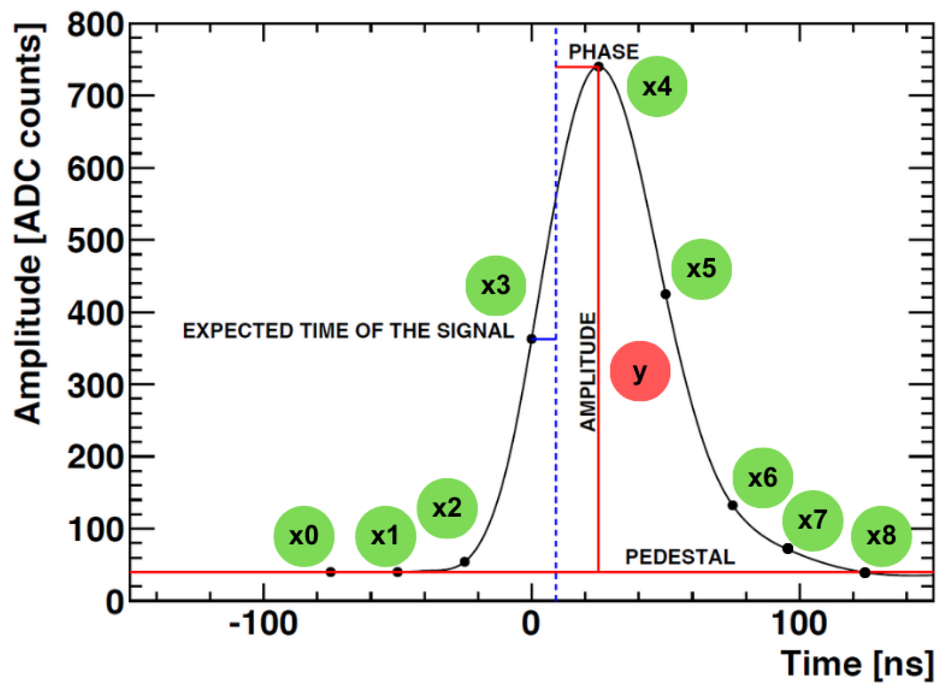
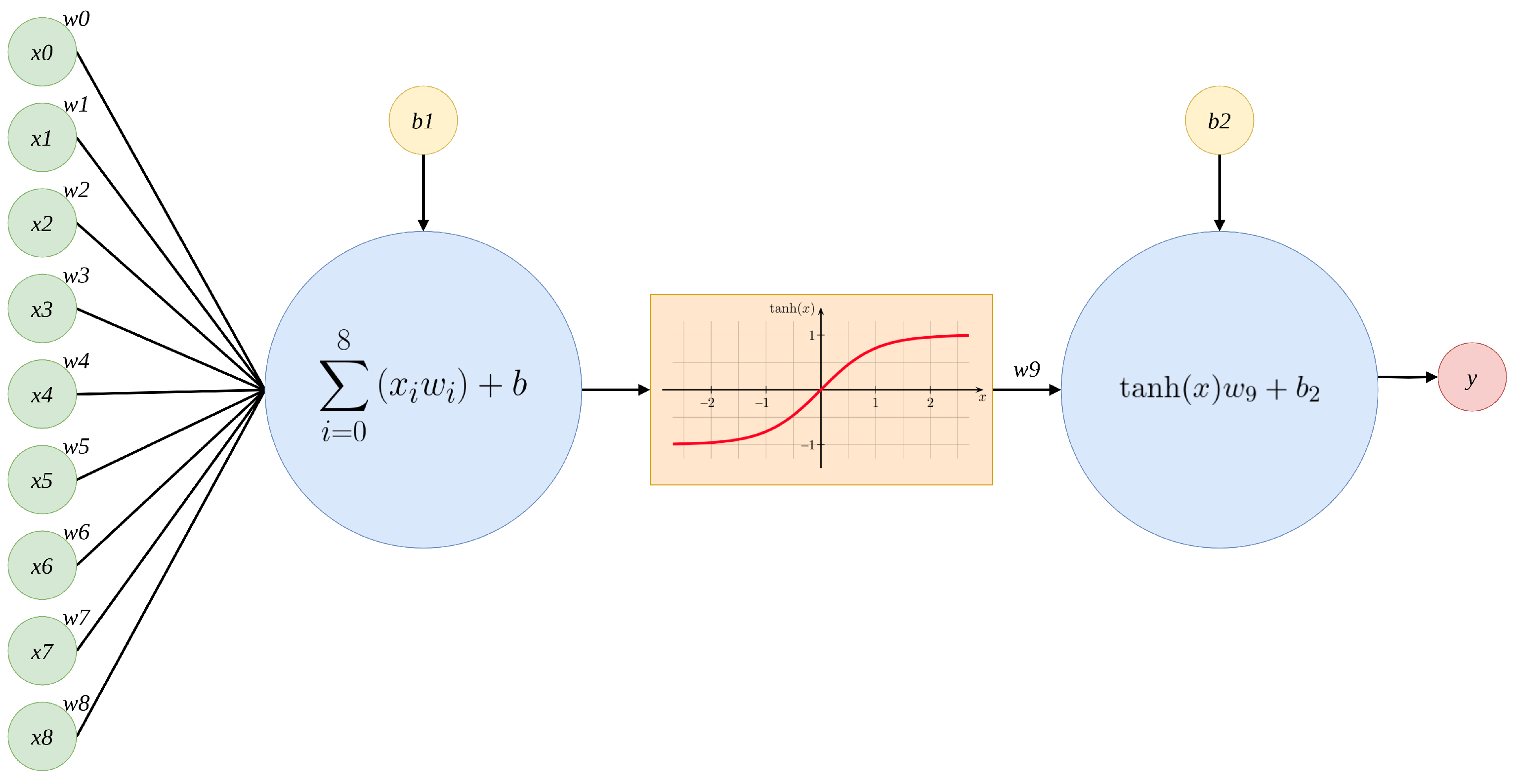
2.2.1. Signal Reconstruction Algorithm
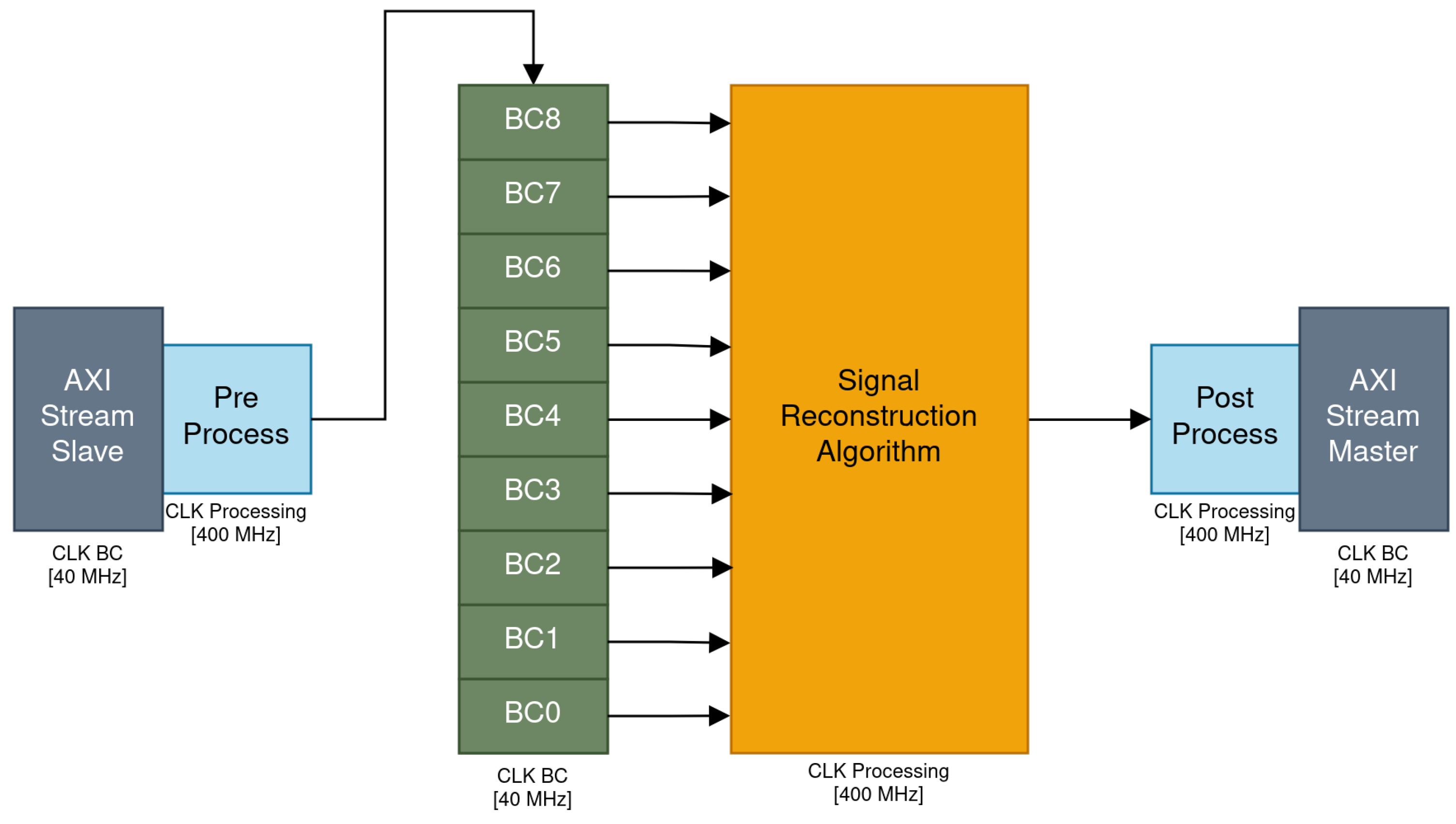
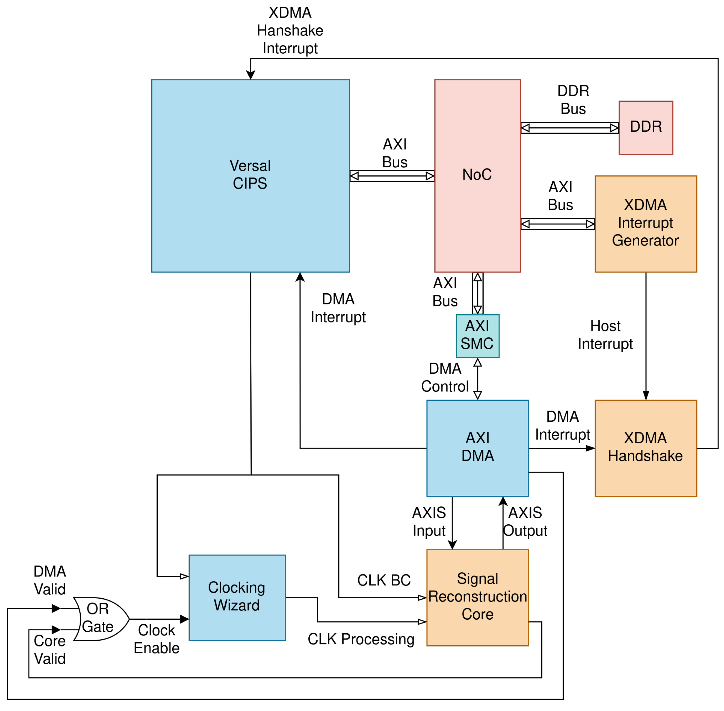
2.2.2. Programmable Logic Integration
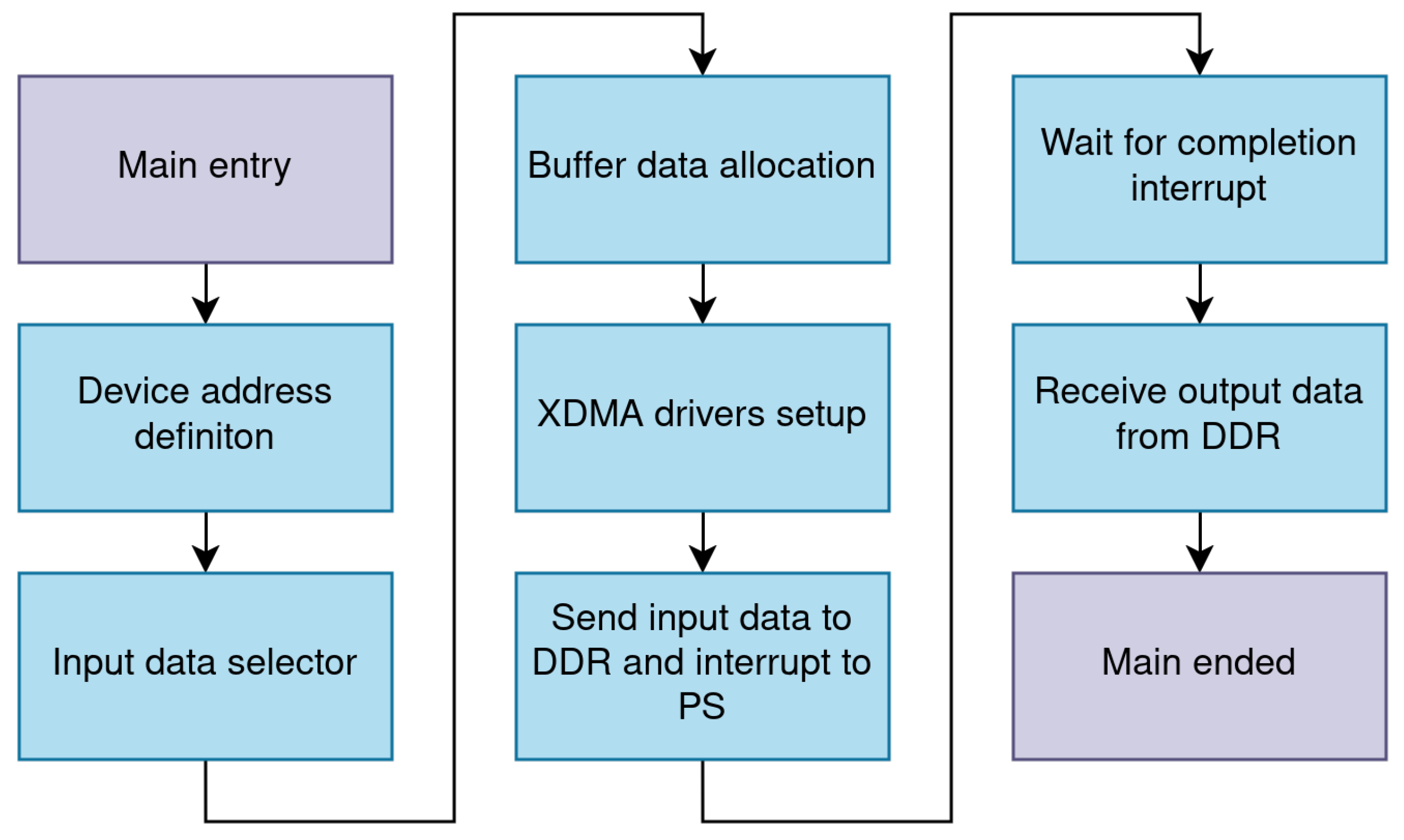
2.3. Software
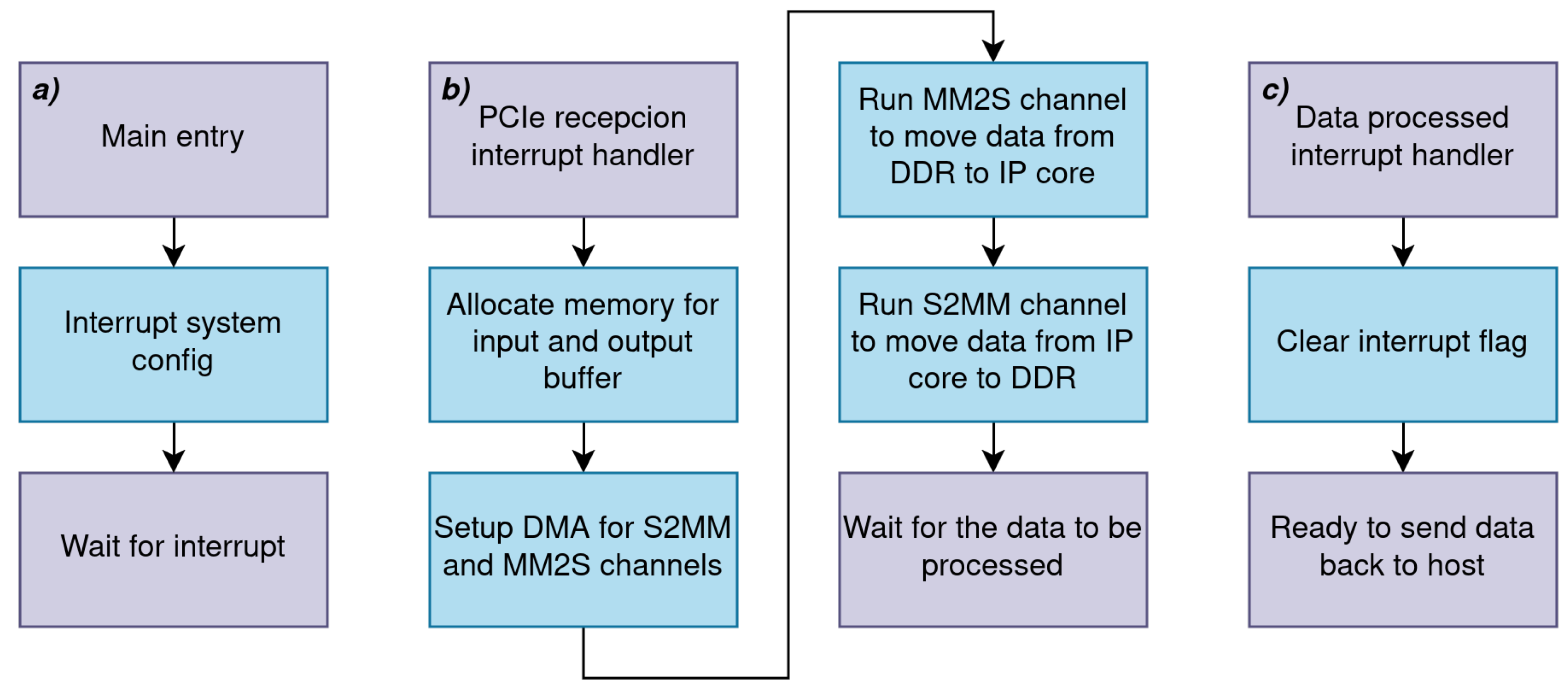
2.3.1. Processing System
2.3.2. Host Drivers
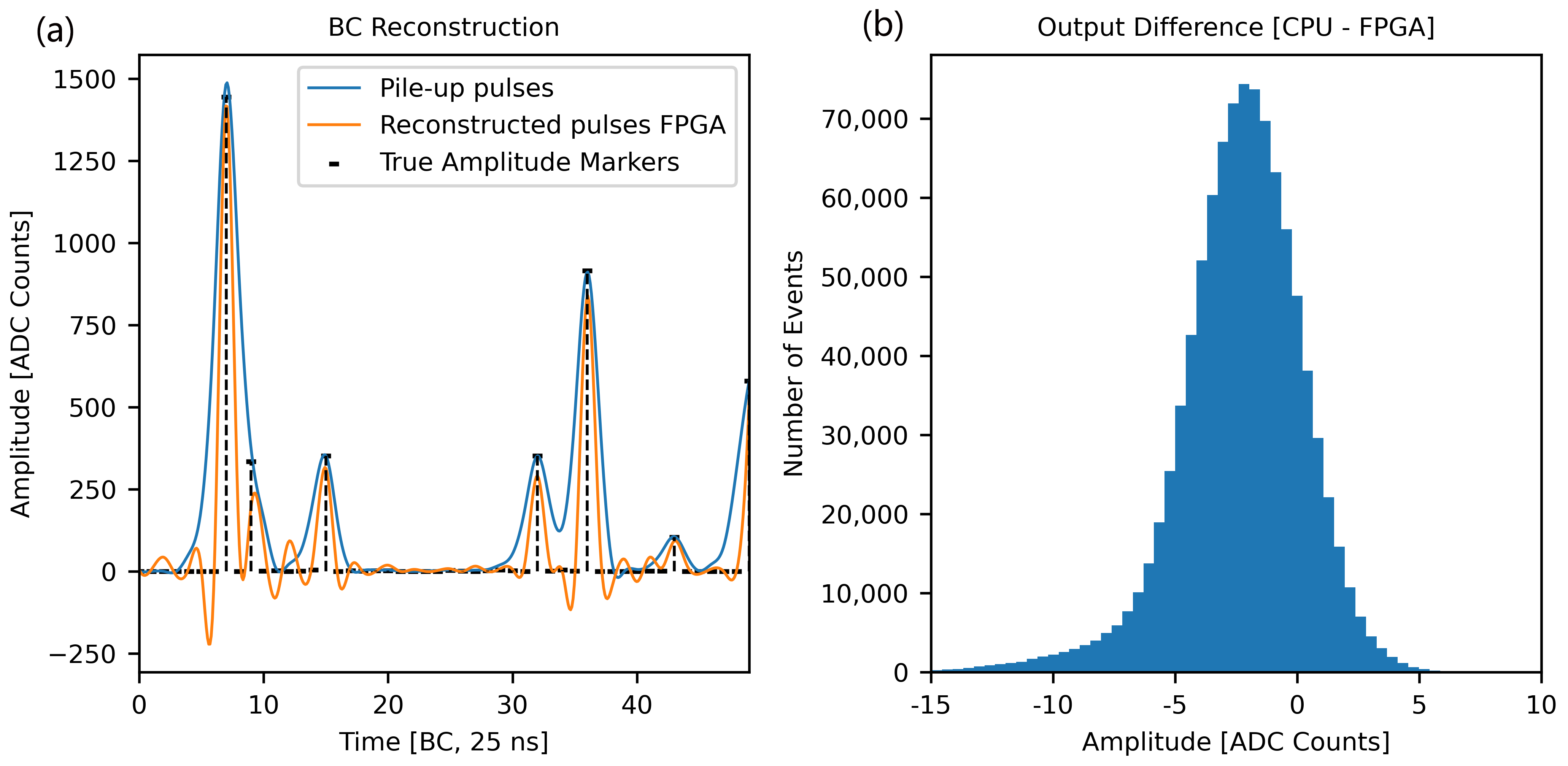
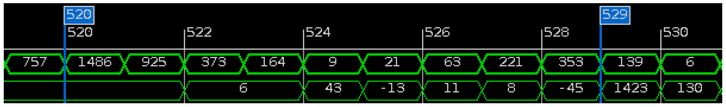
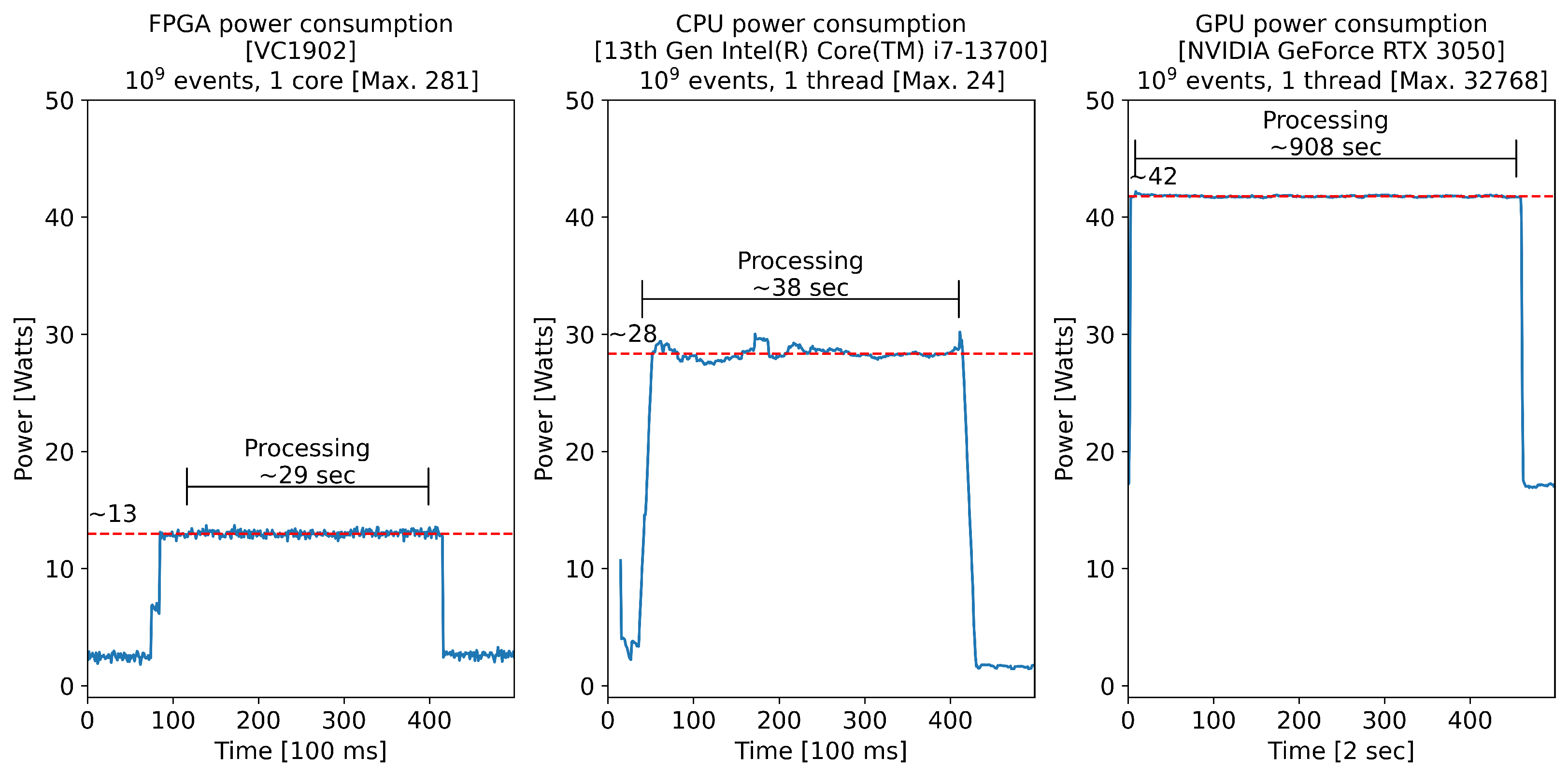
3. Results
4. Conclusions
Author Contributions
Funding
Data Availability Statement
Conflicts of Interest
References
- Brüning, O.S.; Collier, P.; Lebrun, P.; Myers, S.; Ostojic, R.; Poole, J.; Proudlock, P. LHC Design Report; CERN Yellow Reports: Monographs; CERN: Geneva, Switzerland, 2004. [Google Scholar] [CrossRef]
- Aberle, O.; Béjar Alonso, I.; Brüning, O.; Fessia, P.; Rossi, L.; Tavian, L.; Zerlauth, M.; Adorisio, C.; Adraktas, A.; Ady, M.; et al. High-Luminosity Large Hadron Collider (HL-LHC): Technical Design Report; CERN Yellow Reports: Monographs; CERN: Geneva, Switzerland, 2020. [Google Scholar] [CrossRef]
- ATLAS Collaboration. Operation and performance of the ATLAS tile calorimeter in LHC Run 2. Eur. Phys. J. C 2024, 84, 1313. [Google Scholar] [CrossRef]
- Einsweiler, K.; Pontecorvo, L. Technical Design Report for the Phase-II Upgrade of the ATLAS Tile Calorimeter; Technical report; CERN: Geneva, Switzerland, 2017. [Google Scholar]
- AMD-Xilinx. Versal Adaptive SoC Technical Reference Manual (AM011), 1.6 ed.; AMD, Inc.: Sunnyvale, CA, USA, 2023. Available online: https://docs.amd.com/r/en-US/am011-versal-acap-trm (accessed on 15 April 2025).
- AMD-Xilinx. VCK190 Evaluation Board User Guide (UG1366), 1.2 ed.; AMD, Inc.: Sunnyvale, CA, USA, 2024. Available online: https://docs.amd.com/r/en-US/ug1366-vck190-eval-bd (accessed on 15 April 2025).
- Arciniega, J.; Carrió, F.; Valero, A. FPGA implementation of a deep learning algorithm for real-time signal reconstruction in particle detectors under high pile-up conditions. J. Instrum. 2019, 14, P09002. [Google Scholar] [CrossRef]
- ARM. AMBA® AXI Protocol Specification, issue K ed.; Arm Ltd.: Cambridge, UK, 2023. Available online: https://developer.arm.com/documentation/ihi0022/latest/ (accessed on 15 April 2025).
- IEEE Std 1076-2008; IEEE Standard VHDL Language Reference Manual. IEEE: New York, NY, USA, 2009. [CrossRef]

| Resource Type | IP Core Usage | System Usage | Max. Cores |
|---|---|---|---|
| FF (Slices) | 975 | 0.054 % | 1845 |
| LUT (Slices) | 825 | 0.092 % | 1090 |
| PL Memory (kb) | 216 | 0.113 % | 884 |
| DSP (Slices) | 7 | 0.356 % | 281 |
| BC Freq. (MHz) | 40 | - | - |
| Processing Freq. (MHz) | 400 | - | - |
| Bus data width (bits) | 32 | - | - |
| Bandwidth (MB/s) | 160 | 0.156 % * | 640 * |
Disclaimer/Publisher’s Note: The statements, opinions and data contained in all publications are solely those of the individual author(s) and contributor(s) and not of MDPI and/or the editor(s). MDPI and/or the editor(s) disclaim responsibility for any injury to people or property resulting from any ideas, methods, instructions or products referred to in the content. |
© 2025 by the authors. Licensee MDPI, Basel, Switzerland. This article is an open access article distributed under the terms and conditions of the Creative Commons Attribution (CC BY) license (https://creativecommons.org/licenses/by/4.0/).
Share and Cite
Hervás Álvarez, F.; Valero Biot, A.; Fiorini, L.; Gutiérrez Arance, H.; Carrió, F.; Ahuja, S.; Curcio, F. Versal Adaptive Compute Acceleration Platform Processing for ATLAS-TileCal Signal Reconstruction. Particles 2025, 8, 49. https://doi.org/10.3390/particles8020049
Hervás Álvarez F, Valero Biot A, Fiorini L, Gutiérrez Arance H, Carrió F, Ahuja S, Curcio F. Versal Adaptive Compute Acceleration Platform Processing for ATLAS-TileCal Signal Reconstruction. Particles. 2025; 8(2):49. https://doi.org/10.3390/particles8020049
Chicago/Turabian StyleHervás Álvarez, Francisco, Alberto Valero Biot, Luca Fiorini, Héctor Gutiérrez Arance, Fernando Carrió, Sonakshi Ahuja, and Francesco Curcio. 2025. "Versal Adaptive Compute Acceleration Platform Processing for ATLAS-TileCal Signal Reconstruction" Particles 8, no. 2: 49. https://doi.org/10.3390/particles8020049
APA StyleHervás Álvarez, F., Valero Biot, A., Fiorini, L., Gutiérrez Arance, H., Carrió, F., Ahuja, S., & Curcio, F. (2025). Versal Adaptive Compute Acceleration Platform Processing for ATLAS-TileCal Signal Reconstruction. Particles, 8(2), 49. https://doi.org/10.3390/particles8020049