2. General Theory and Characterization Technique
Induced phase noise characterisation methods as well vibration sensitivity figure of merit for filters [
3,
4] are available, but from these it is not easy to directly infer behavioural models of discrete microwave filters. Usually, manufacturers perform vibration and shock tests according to international standards [
5,
6,
7] in order to certify that the devices meet electrical performance
after the trials [
8], but sometimes evidence of correct operation of the device is required
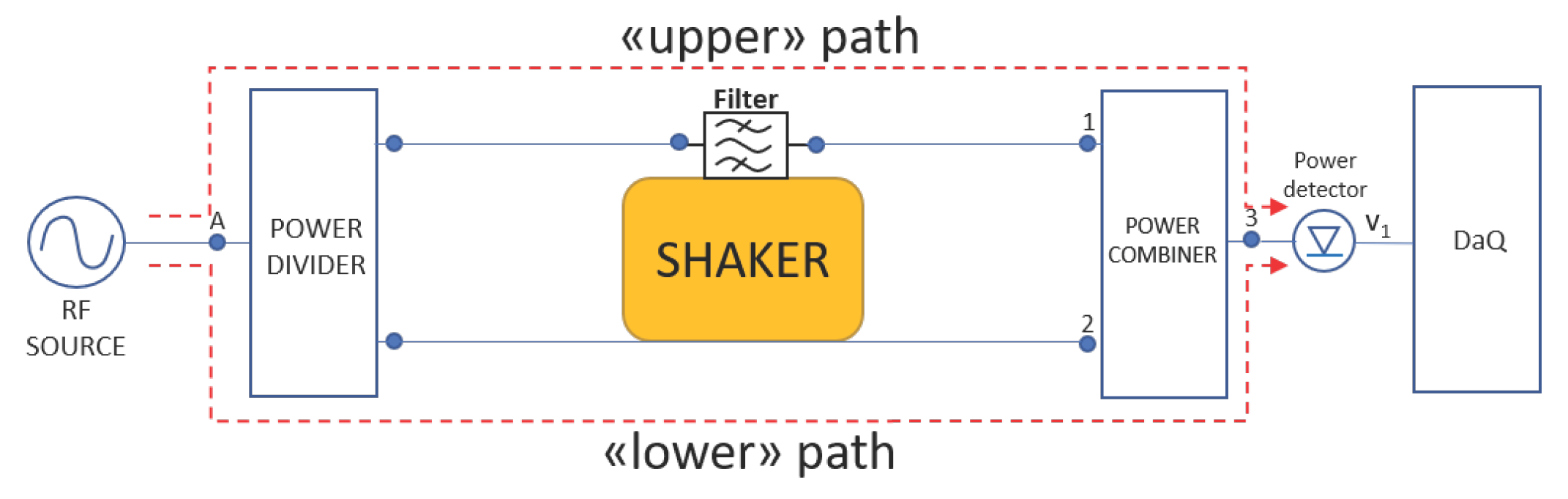
during the application of the solicitation. A filter subjected to vibrations can be reasonably treated as a transducer so that external induced vibrational energy is partially transformed in simultaneous amplitude and phase modulation of the input RF or IF signal. The signal bandwidth is supposed to be much wider than the vibration induced modulation bandwidth. The theory of operation can be understood by referring to the test-bed reported in
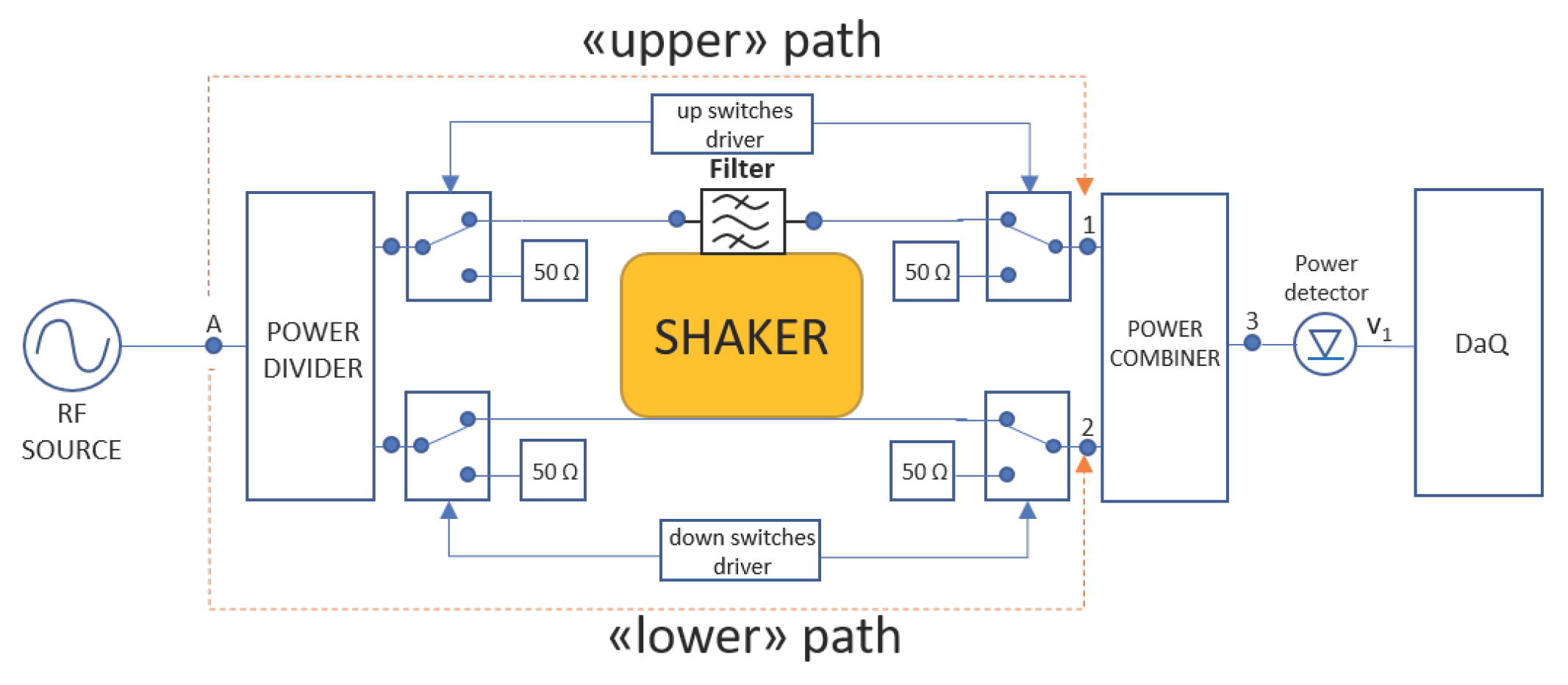
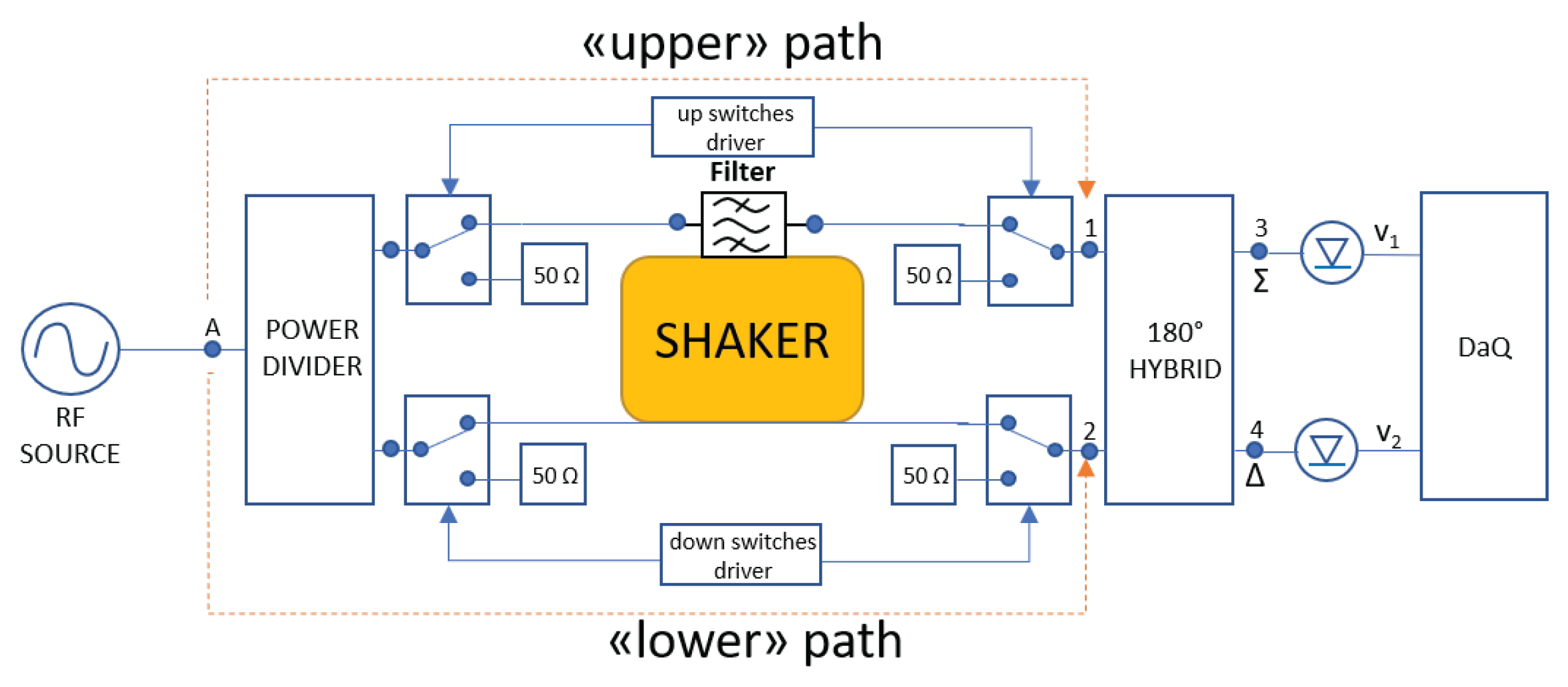
Figure 1. Using a compact complex envelope notation [
9], the RF source generates an in-band CW (Continuous Wave) signal:
at node
A of the circuit, where it is splitted in two paths:
upper and
lower. The signal in the
upper path flows through the filter where emerges modulated both in amplitude and phase due to the vibrational energy as:
with
. The signal in the
lower path flows in a through-line and recombines with the signal coming form the
upper path in an isolated RF combiner. The signals flow is regulated by two couples of SPDTs (Single Pole Double Throw) in order to provide high isolations level: the first couple controls the
upper path; the second couple controls the
lower path. Each couple of SPDT is driven by a dedicated driver. The signal from the output RF combiner is injected in a zero bias schottky detector whose output signal, being eventually conveniently amplified by a low noise stage, is acquired. A dedicated fixture is designed and fixed to the shaker to allow vibration tests to be performed. The filter, generally available in a SMT package (Surface Mount Technology), is soldered over a microstrip circuit with dedicated input and output connectors. A microstrip through line is located near the filter with its own input and output connectors. So, two input ports and two output ports are available on the test jig, each circuit is independent from the other but both shares the same vibrational energy. Following the scheme, it is possible to note that the jig, fixed to the shaker, is connected to the isolated RF power divider and combiner using phase invariant coaxial cables so that when the SPDTs are driven as in
Figure 2, it is possible to identify an
upper and
lower path, where the input signal is first splitted and then recombined. Using the superposition principle, the input signal to the power detector due to the
upper path is:
where:
is the transmittance from port A to port 3 through the upper path when there is no vibration
is the instantaneous transmittance of the filter under vibrations and is a real valued function.
While the input signal to the power detector due to the
lower path is:
where:
is the transmittance from port A to port 3 through the lower path when there is no vibration
is the instantaneous transmittance of the microstrip line under vibration, being a real valued function.
So, the
recombined output signal arising from the RF combiner can be put in the form:
this signal is injected in a zero bias schottky detector, whose output signal is of the form:
where
is the detector’s sensitivity and
the instantaneous power of the RF input signal. When the system is under vibration, the instantaneous output signal is:
while, when no vibrational energy is injected to the system:
so,
, is time independent. If the filter’s microphonicity is negligible, the output signal is constant. If the microstrip circuit, that’s part of the
lower path, can be assumed to be quite insensible to vibrations, it is possible to simplify the output signal as:
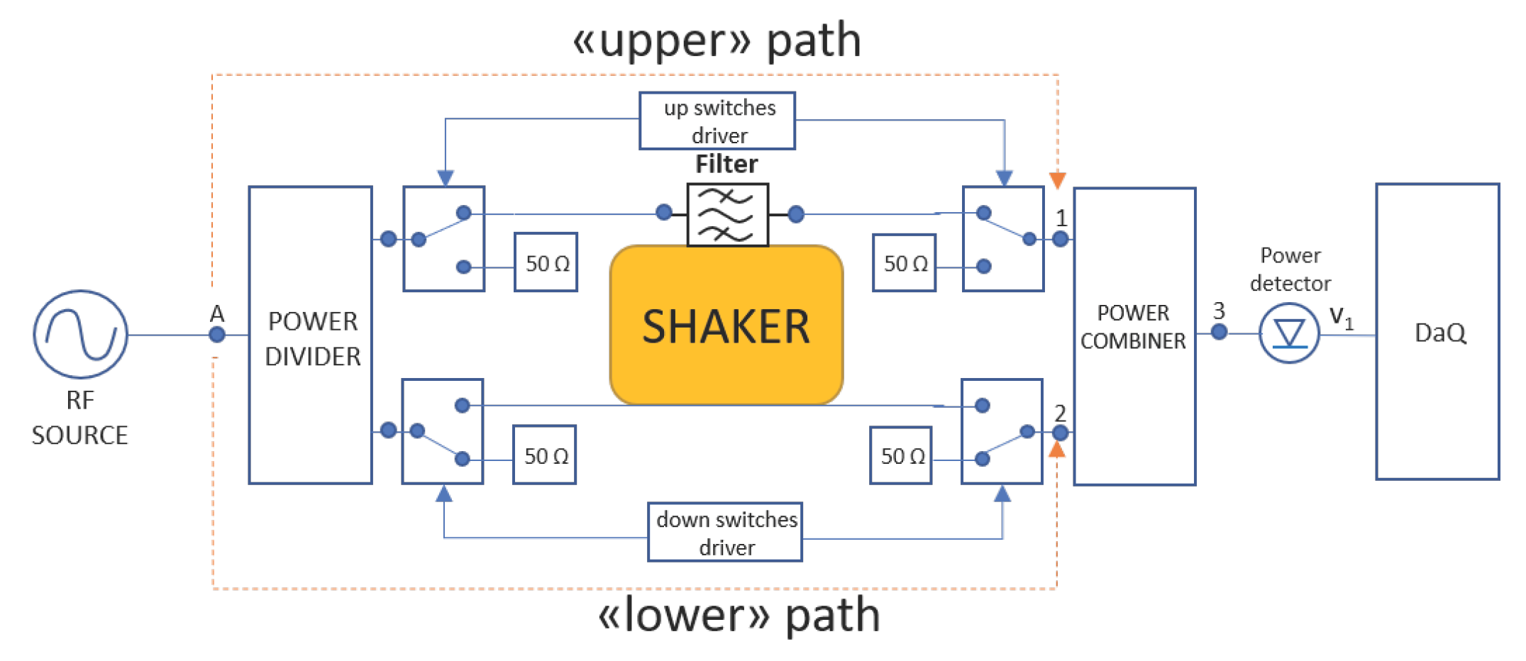
now, when the SPDT couple of the down path is driven in order to open the signal’s flow, the test-bed is equivalent to
Figure 3.
The output signal, under vibration, is:
while, in static conditions:
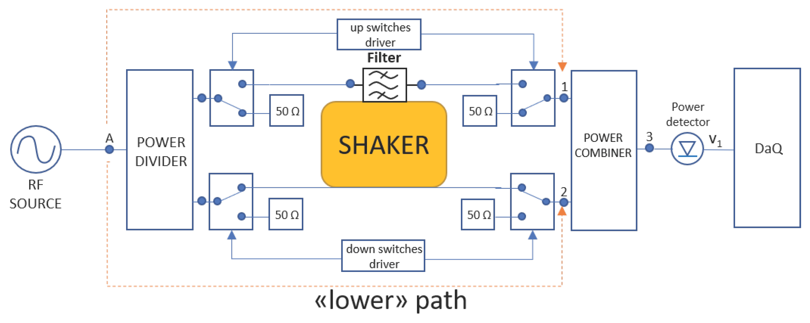
when the SPDT couple of the
upper path is driven in order to open the signal’s flow, the test-bed is equivalent to that reported in
Figure 4.
The output signal, under vibration and in static condition, is:
so the filter amplitude modulation, if present, constitutes the signal:
If the DC component is prevalent, then the amplitude modulation is negligible and
. Under these conditions the signals:
,
,
are DC voltages and the phase induced modulation function
is recoverable from the output signal:
apart from a constant phase term
. The vibration induced phase modulation
is transformed in a
amplitude modulation of the low frequency signal
, so a wise choice of the phase term
allows to maximize the signal’s dynamic range. If the low signal phase difference between upper and lower paths
with
, than the slope of the cosine function in Equation (
14) is maximized. Changing the vibrational sine frequency, it is possible to extract the relative induced phase modulation and the characterization process can be fully automated.
2.1. System Simulation and Validation
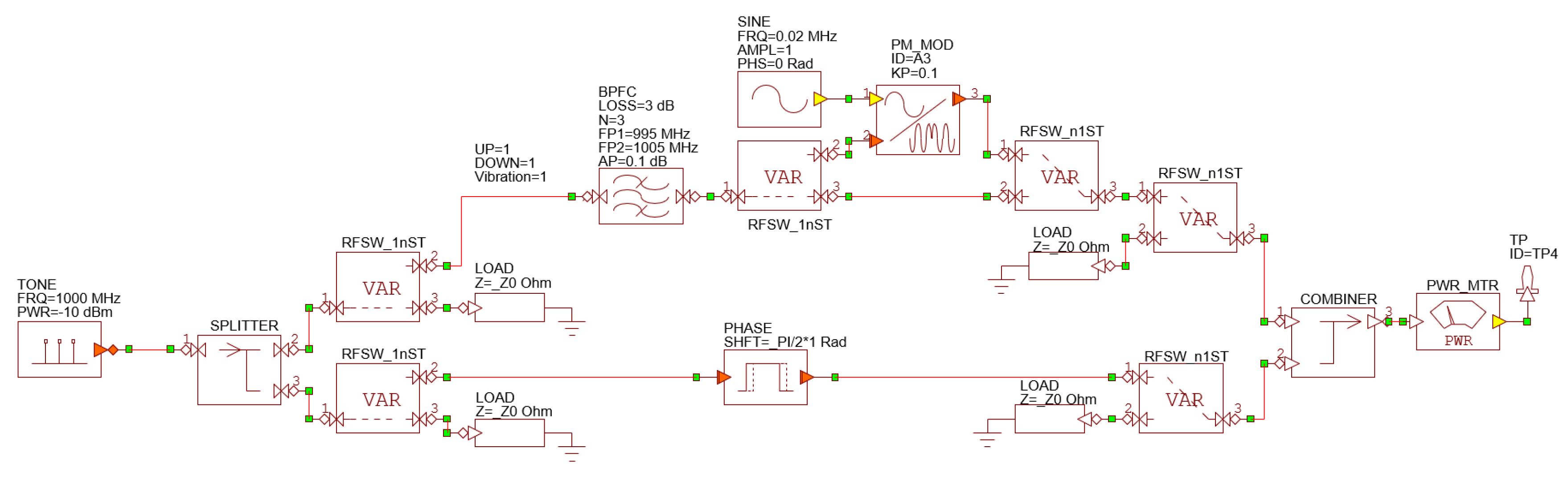
The theoretical approach has been validated through RF system simulations using NI AWR VSS Visual System Simulator™ [
10] and MATLAB
® [
11]. The NI AWR VSS schematic is reported in
Figure 5 and includes, in a more detailed form, the characterisation set-up depicted in
Figure 3 and
Figure 4.
A signal generator injects a −10 dBm CW tone at 1 GHz into a power divider where it is divided in two branches. The upper path contains an RF filter, in this case a 3 poles, 10 MHz bandwidth Bandpass Chebyshev type 1 filter with an insertion loss of 3 dB, followed by a
phase modulator that represents the induced phase modulation due the vibrational energy. The vibration induced phase modulating signal is a 20 KHz unit amplitude sine wave injected in a phase modulator with a phase sensitivity coefficient
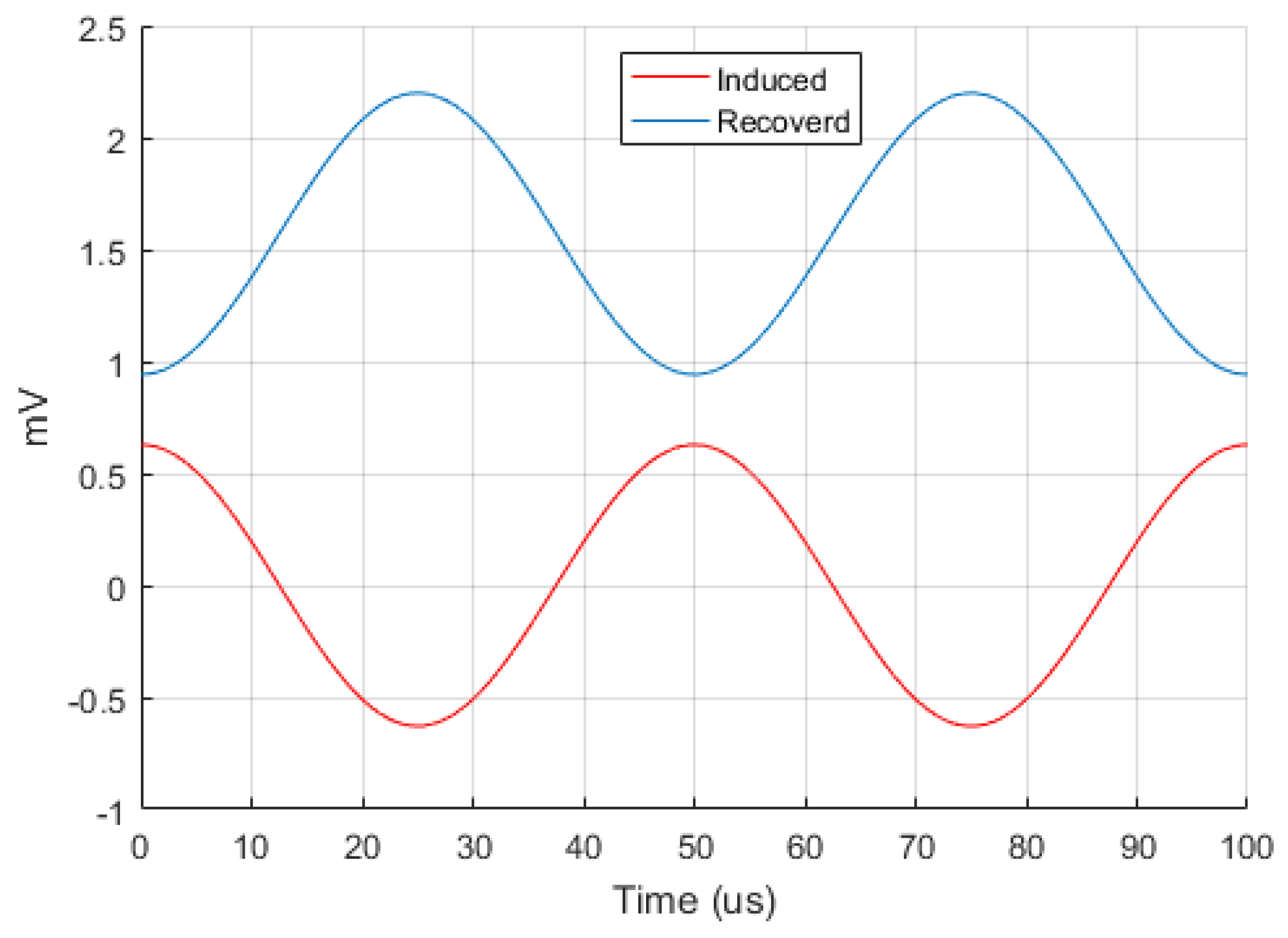
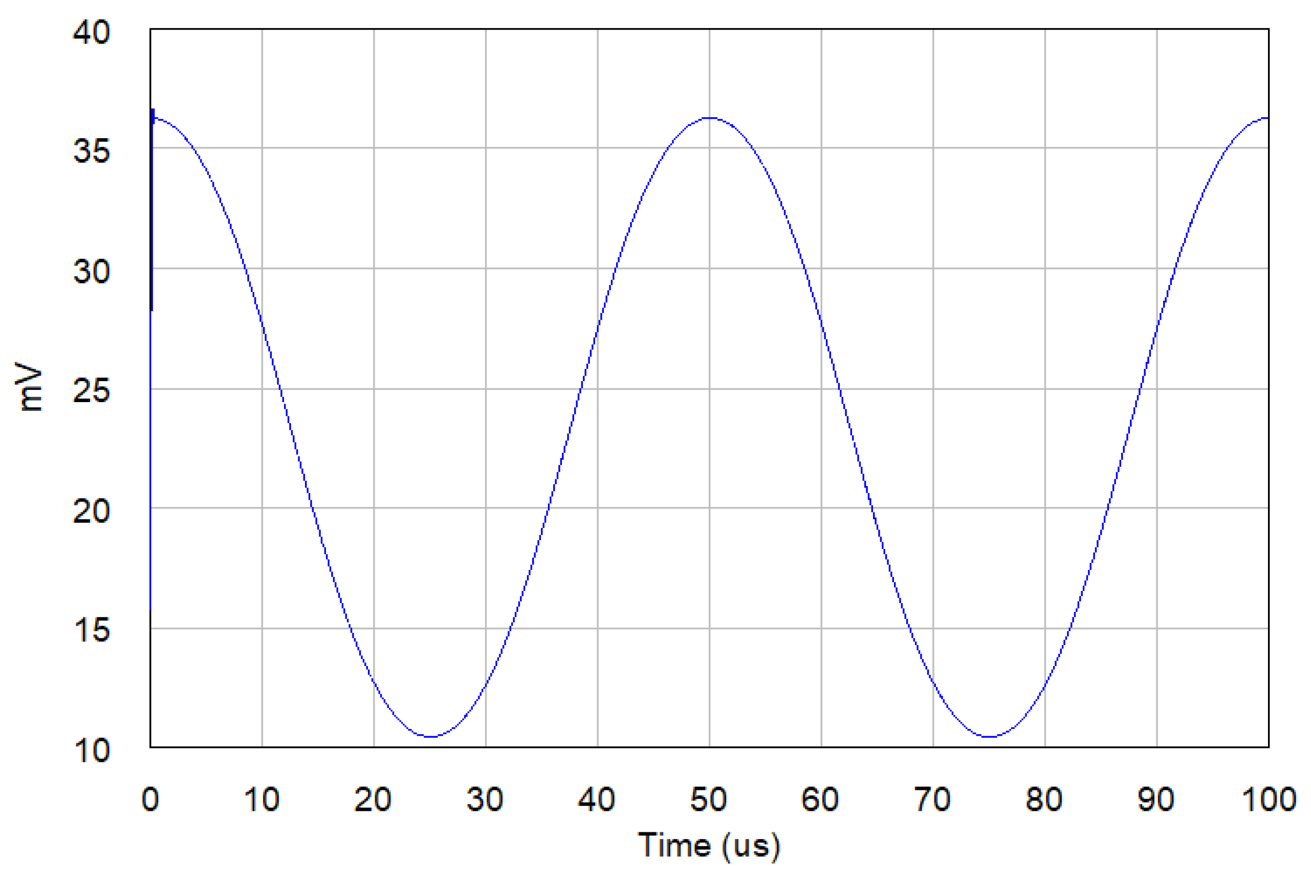
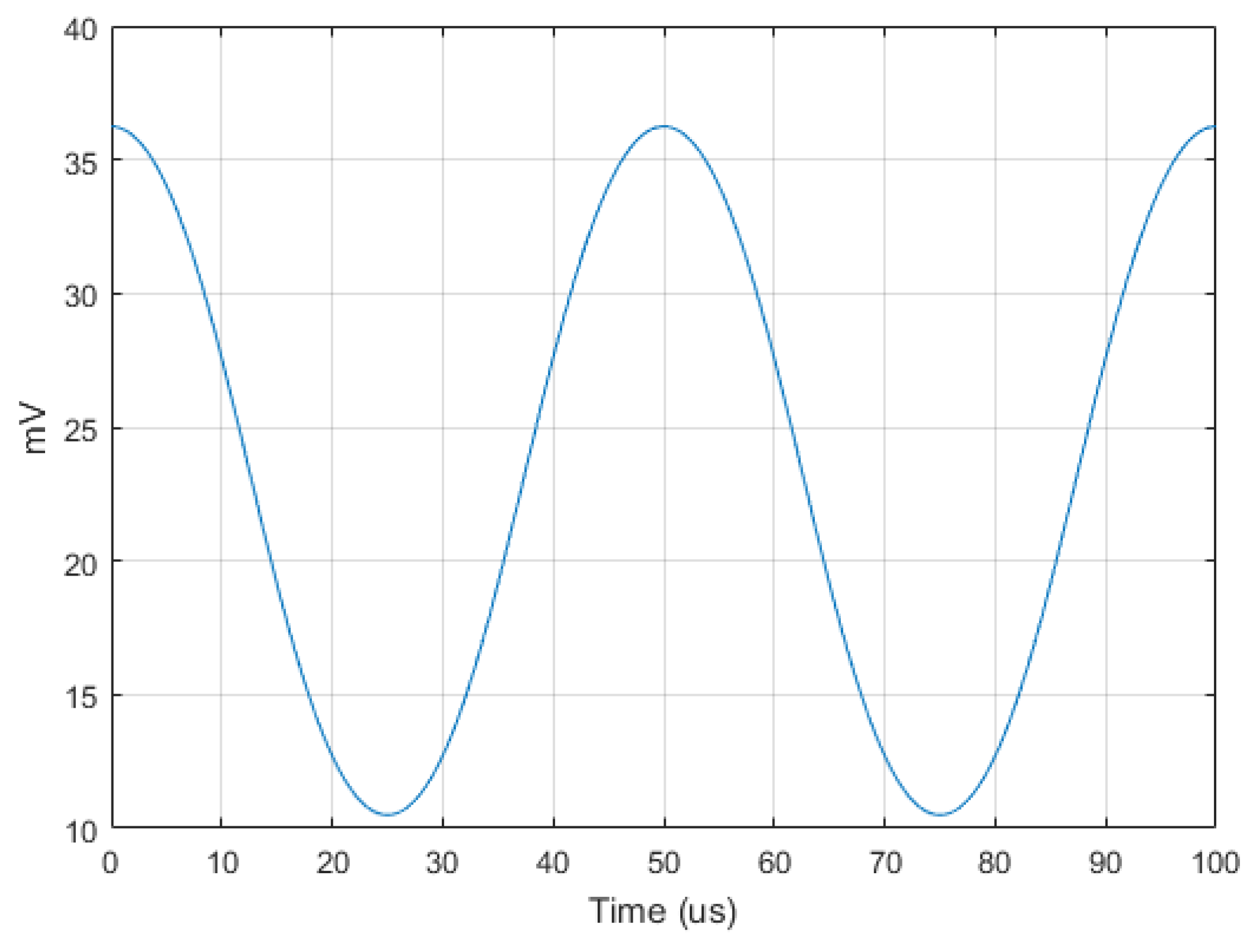
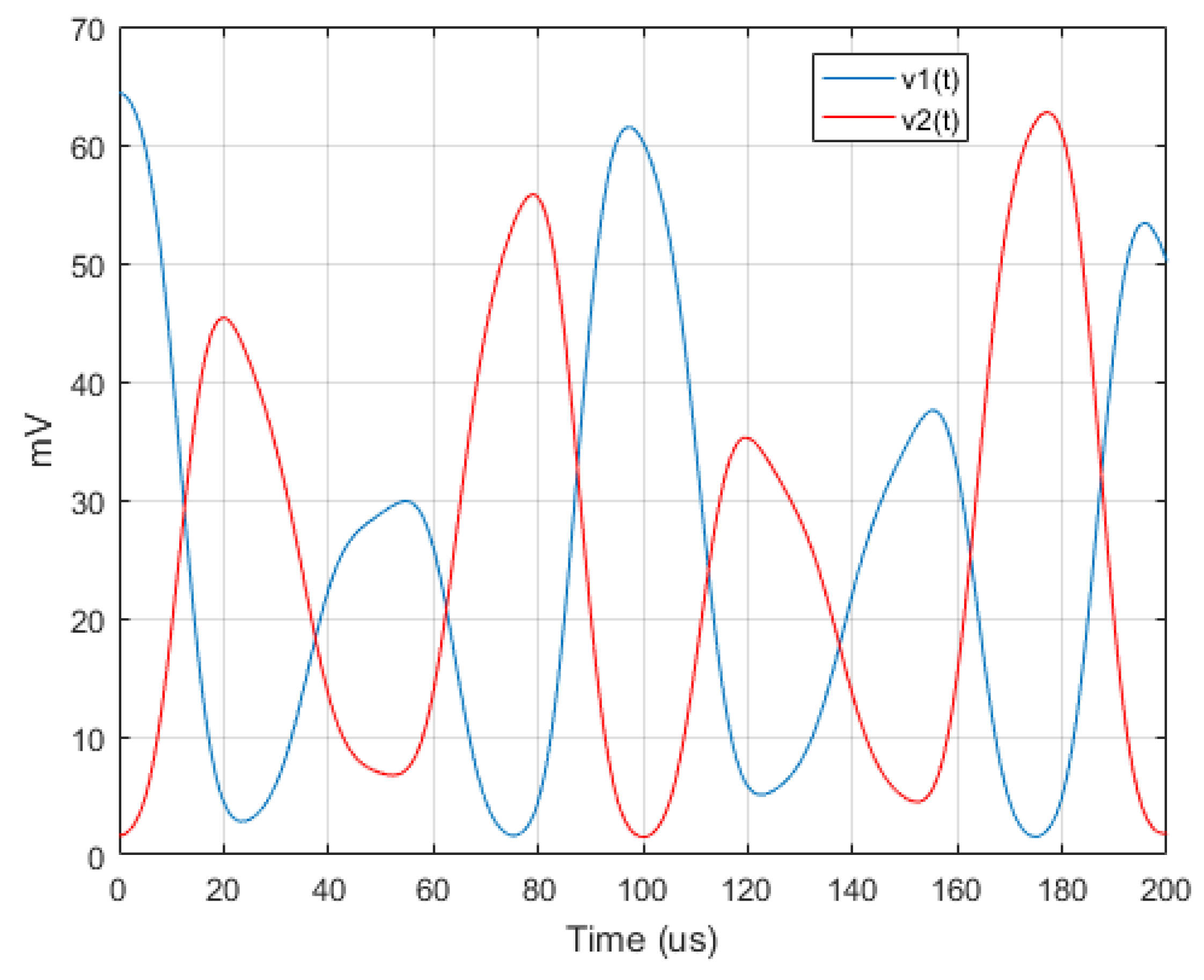
. The presence or absence of vibrations and the path selection is performed by dedicated SPDTs whose insertion loss take into account the additional losses introduced by the cables also. The lower path contains the dedicated branch selection SPDTs, cable and a RF phase shifter. The signals arising from the upper and lower paths are injected in a RF combiner whose output port is terminated in a power detector. The low frequency signal from the power detector, described by Equation (
14) is reported in
Figure 6, the same signal exctracted using the Matlab model is reported in
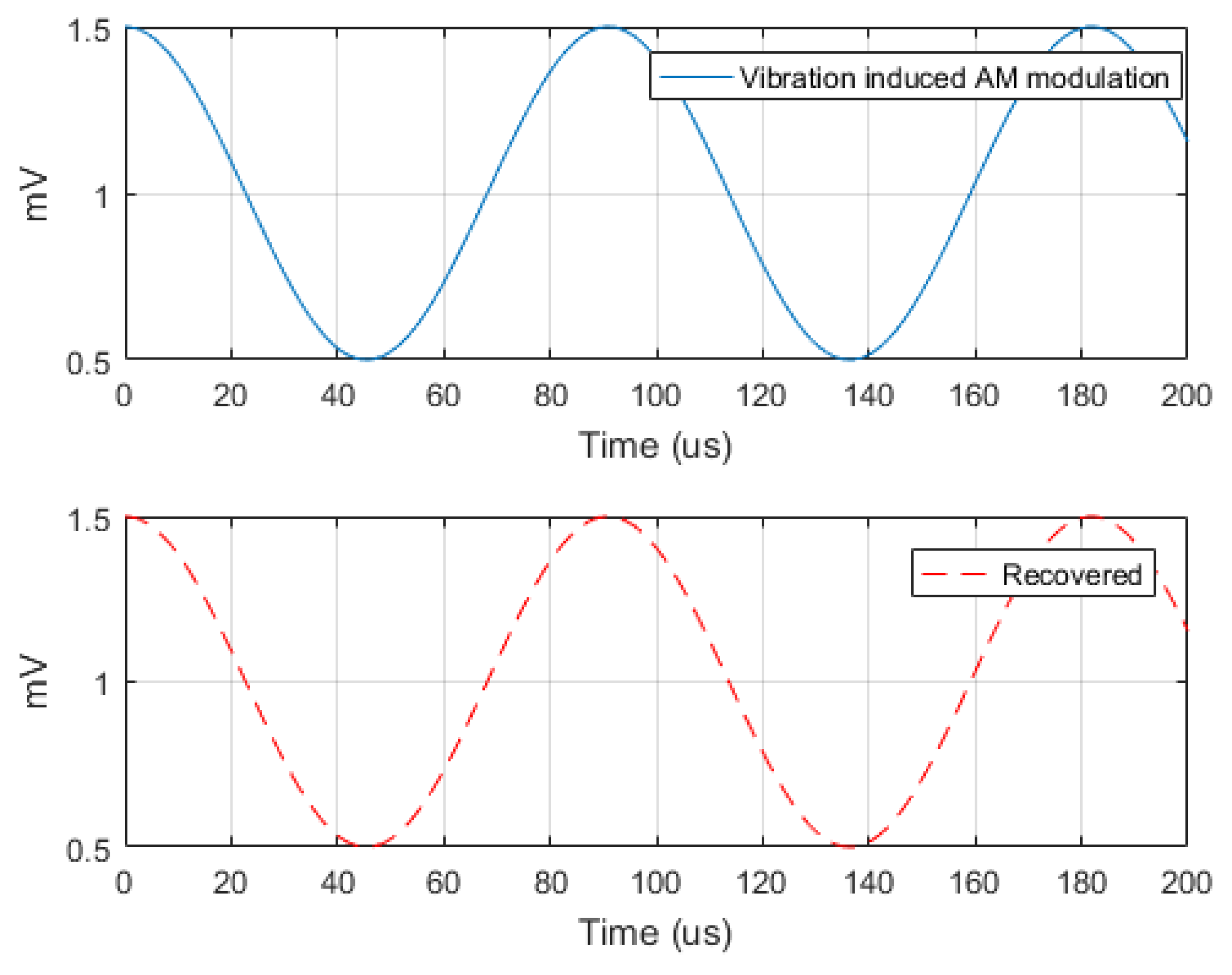
Figure 7 with an excellent agreement between both models. The induced phase modulating signal and the recovered signal are depicted in
Figure 8.
2.2. Extension to Weak Time-Dependent Amplitude Modulation Case
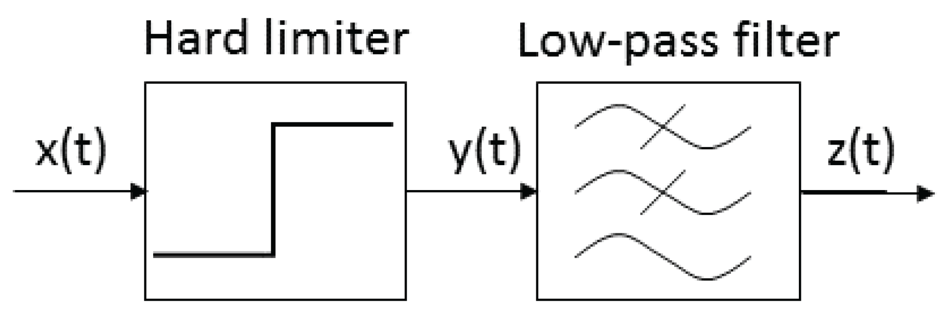
If the induced amplitude modulation is time-dependent, a signal processing approach can be adopted in order to extract the induced phase modulation. If
a more precise technique can be exploited, deleting the DC terms in (
9) in post-processing. In fact, looking at
Figure 9, if a generic low pass signal:
is injected in a hard limiter, the corresponding output signal can be put in the form:
The function
y(t) is periodic in
, so the corresponding Fourier series expansion can be written as:
with coefficients:
a low-pass filter eliminates the high order harmonics so that
this allows to easily extract the phase induced modulation function.
3. High Induced Amplitude Modulation Case
When the induced amplitude modulation function
is not negligible, it is necessary to modify the test-bed in order to be able to extract the phase and the amplitude modulating functions. To this purpose, the output RF combiner is replaced by a 180° hybrid where two different power detectors are connected to the
and
ports. The output signals arising from the power detectors, eventually conveniently amplified by low noise stage amplifiers, are injected in a simultaneous sampling DaQ (Data Acquisition device). Looking at
Figure 10, if the RF source generates a signal of the form (
1), the signals arising from the power detectors are:
where
are the modules of the trasmittances of the 180° hybrid and
are the modules of the trasmittances of the
upper path from node
A to node
1 and
lower path from node
A to node
2 respectively. In general, the detectors sensitivity coefficients k
and k
, the parameters S
, S
, S
, S
are different, even slightly, from each other. Opening the
upper path in static conditions (no vibrations), the output voltages from the detectors are constants, respectively equal to:
closing the
upper path, while opening the
lower, the output voltages from the detectors are constants and respectively equal to:
Variables
A,B,C,D have been introduced only to simplify the expressions in
static conditions and allow compact notations. When vibrations are present, and both
upper and
lower paths are closed, the signals from the detectors are time dependent and respectively equal to:
after some algebraic manipulations, it is possible to write:
while the phase induced modulation is:
where
are constant and vibration independent phase terms.
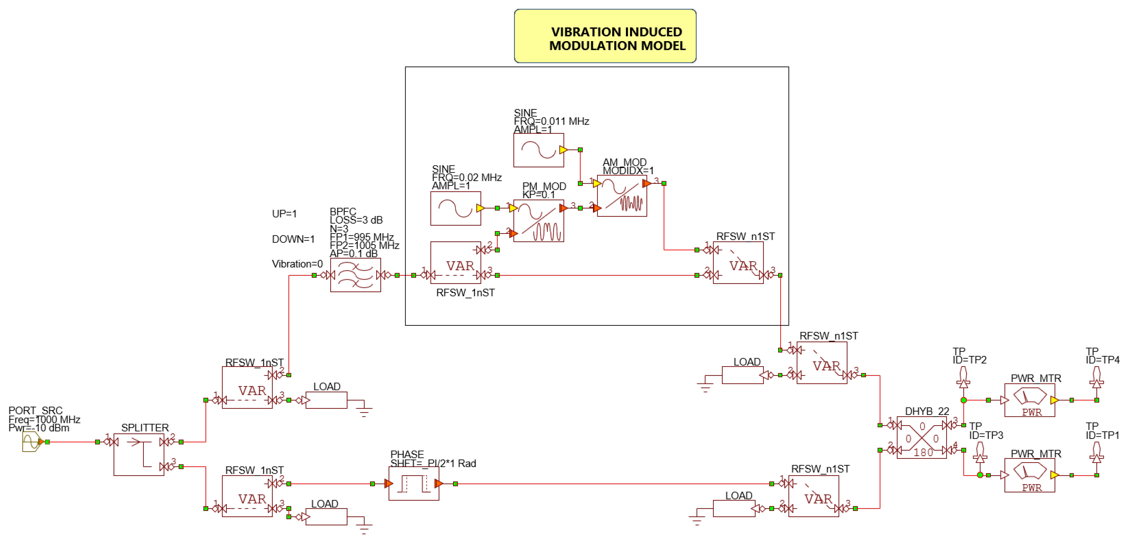
System Simulation and Validation
This characterisation method, as the simpler described before, has been validated through RF system simulations. The NI AWR VSS schematic is reported in
Figure 11 and includes, in a more detailed form, the characterisation set-up depicted in
Figure 10.
The first part of the scheme is similar to that reported in
Figure 5 with two main differences: after the RF filter there are two separated amplitude and phase modulators, each of these modulates the RF signal indipendently from the other with different modulation frequencies and modulation indices. The signal travelling the upper path and that travelling the lower path recombines into a 180° hybrid coupler. The
and
output signals are then injected in two RF power detectors whose output voltages have been stored and processed. The vibration induced phase modulating signal is a 20 KHz unit amplitude sine wave injected in a phase modulator with a phase sensitivity coefficient
. The vibration induced amplitude modulating signal is a 11 KHz unit amplitude sine wave injected in a amplitude modulator with a normalized sensitivity coefficient
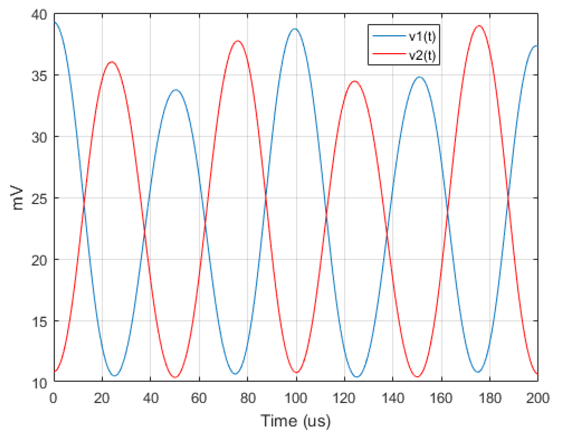
. The amplitude and phase modulating frequencies are not harmonically related and have been choosen different in order to verify the correct recover of both. The output voltages from the power detectors
and
under vibrations are reported in
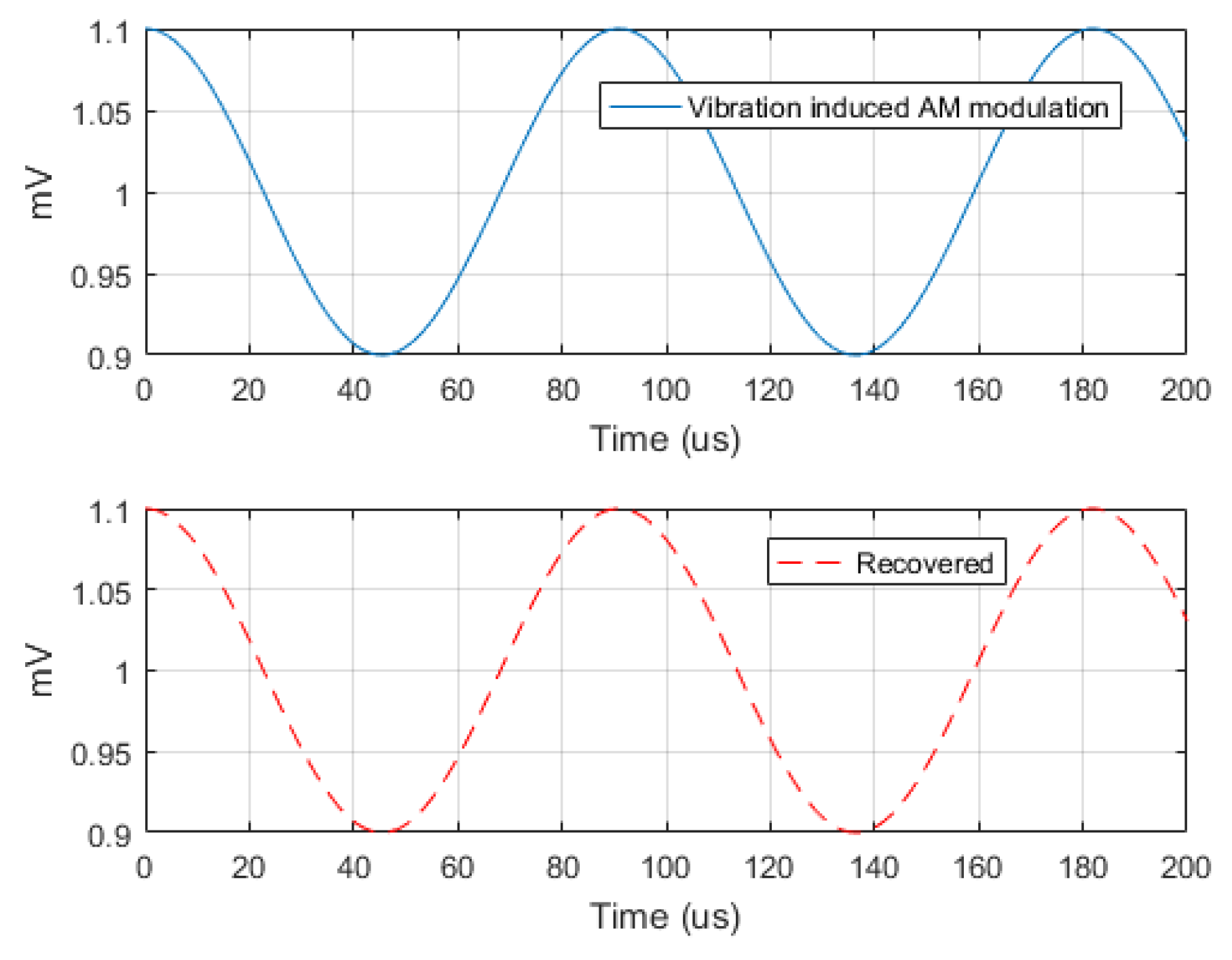
Figure 12 while the induced amplitude modulating signal and the one recovered are reported in
Figure 13.
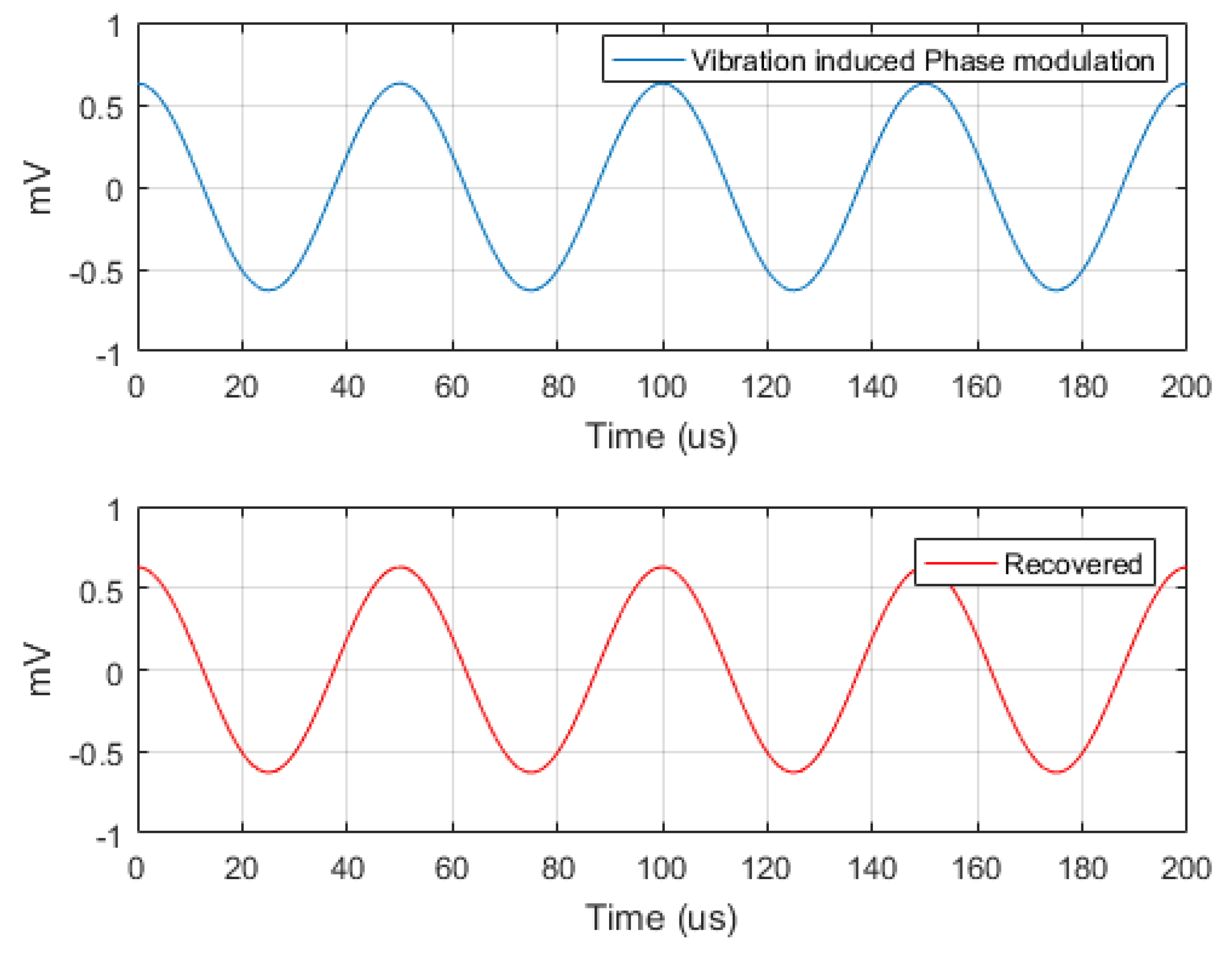
The induced phase modulating signal and the one recovered are reported in
Figure 14.
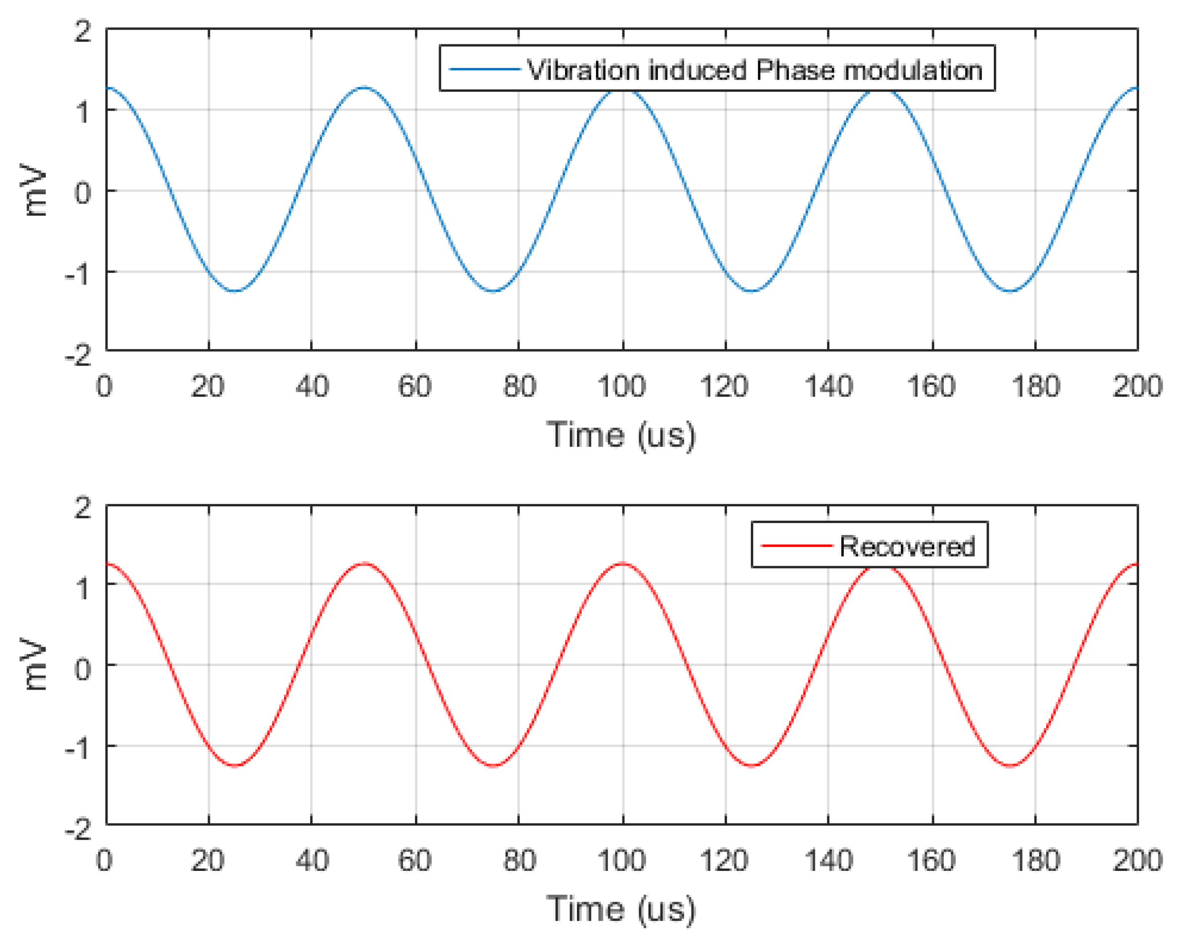
For a fixed vibrational frequency, a change of the vibrational energy is modeled as a corresponding change of phase and amplitude modulation indices. If the amplitude and phase modulation indices are raised to
and
respectively, the output voltages from the power detectors
and
are reported in
Figure 15.
The induced amplitude and phase waveforms and the recovered signals are reported in
Figure 16 and
Figure 17.
It is noteworthy that the quantities: can be frequency dependent, but all of them can be characterized in the frequency domain, if necessary. The quantities are also allowed to be temperature-dependent as these are directly related to the transmittance of the filter under test. Moreover, the proposed method does not require a sinusoidal vibrational spectrum in order to extract the amplitude and phase induced modulations, but it can be theoretically arbitrary.
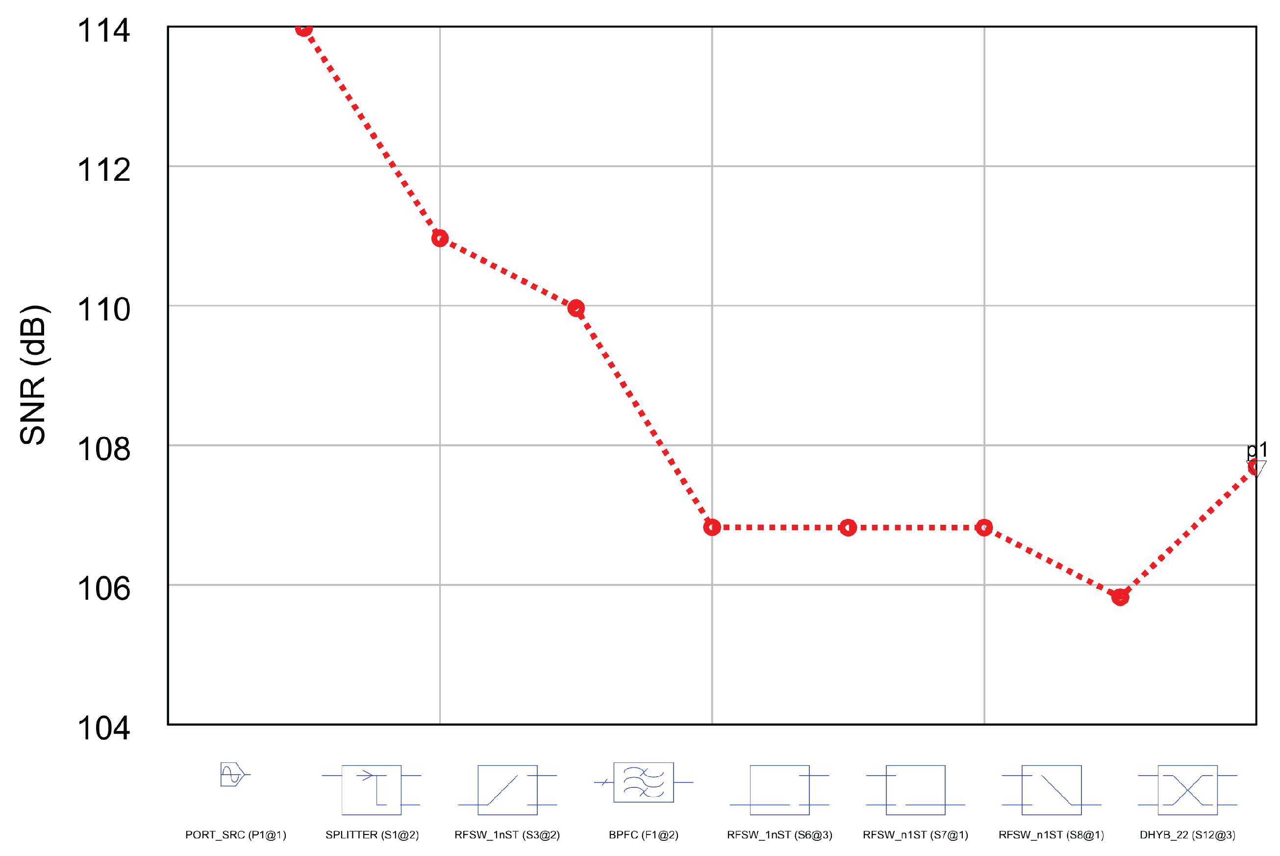
4. System Sensitivity Considerations
All the schemes discussed in previous sections works at high Signal to Noise Ratios by design, insertion losses of the devices are quite small even that of SAW filters (usually
dB). The input signal is provided by a RF source with a very high SNR (Signal to Noise Ratio) while power detectors operate with signal levels
dB higher their typical tangential sensitivity [
12]. Limiting the analysis to the induced phase modulation recovering, it is possible to focus the attention to Equation (
14) reported below for convenience, in order to derive some considerations.
If the term
, than it is possible to write
the induced phase modulation
can be assumed to be
, being
the vibration frequency. As vibrational induced phase modulation comes from low frequency mechanical excitation (sometimes up to acoustic frequencies), it is reasonable to suppose [
13] that the bandwidth
of the signal (
29) is limited to
KHz. The estimated SNR at the output port of the RF combiner (or the output ports of the 180° hybrid) is reported in
Figure 18. It can be assumed that the low frequency signal, acquired by the DaQ, is mainly contaminated by thermal noise coming from the RF section and by the intrinsic thermal noise of the device. The noise power from RF stages is
−124 dBm corresponding to a RMS noise voltage
μV. The RMS noise voltage of a DaQ is tipically much higher. For example, the National Instruments 6356 [
14] in the smallest input voltage range, is characterized by a RMS noise voltage
μV, so it is prevalent over the contribution due the RF section.
Small values of
push the system to the limit of sensibility as
tends to a DC value, but at the same time,
makes the filter able to operate in a severe environment. If
is small, it is possible to approximate the sine function in Equation (
30)
the signals measured experimentally can be written as:
where
,
,
are indipendent zero-mean gaussian noise components having the same standard deviation
. As we searching for the minimum detectable phase modulation index
, the problem is reduced to the estimation of the amplitude of the induced modulating tone at the vibrational frequency
. In fact, it is possible to write
being
n a gaussian noise contribution with power
. In this case, a powerful tool is represented by the FFT (Fast Fourier Transform). If the DaQ operates at a sample frequency of
Hz and
N samples are acquired for each signal, the FFT of the signal reported in Equation (
35) generates
points in the frequency domain where every frequency "bin" is
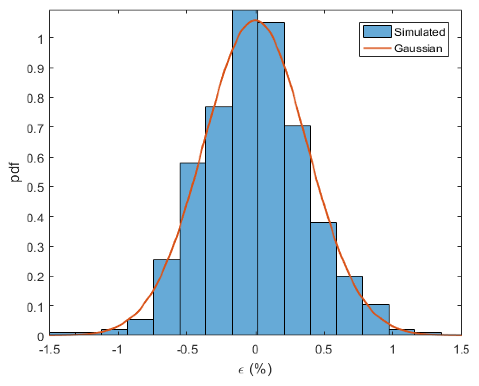
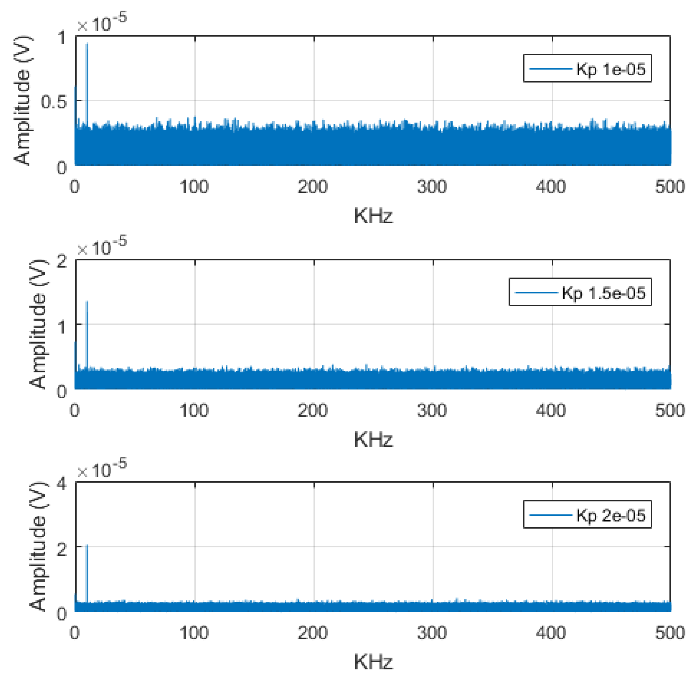
Hz wide. A Matlab simulation has been used to estimate the parameter
with a relative error
in order to define the minimum detectable phase sensitivity coefficient
. The vibrational frequency has been set
KHz with a DaQ sample frequency
MHz. The effective system
where
is the signal power and
the processing gain of the FFT. The magnitude of the spectrum at the frequency “bin” corresponding to the vibrational frequency has been calculated while sweeping the parameter
, thus changing the SNR of the system and determining the relative error; the procedure has been iterated in order to obtain a distribution of the error. Some amplitude spectra are reported in
Figure 19 for different values of
while in
Figure 20 is reported the estimated probability density function (pdf) of the relative error (nearly gaussian) corresponding to the identified minimum detectable
.
From simulations it has been found a minimum detectable phase sensitivity coefficient rad/V with relative errors within .

