Article

Plasma Deposition to Improve Barrier Performance of Biodegradable and Recyclable Substrates Intended for Food Packaging

1
CNR, Institute for Plasma Science and Technology, Via R. Cozzi 53, 20125 Milan, Italy
2
Dipartimento di Fisica, Politecnico di Milano, Piazza Leonardo da Vinci 32, 20133 Milan, Italy
3
Center for Nano Science and Technology @PoliMi, Istituto Italiano di Tecnologia, Via G. Pascoli, 70/3, 20133 Milan, Italy
4
Dipartimento di Fisica, Università di Genova, Via Dodecaneso 33, 16145 Genova, Italy
5
CNR, Institute for Photonics and Nanotechnologies, Piazza Leonardo da Vinci 32, 20133 Milan, Italy
6
CNR, Institute of Condensed Matter Chemistry and Technologies for Energy, Via R. Cozzi 53, 20125 Milan, Italy
*
Author to whom correspondence should be addressed.
Plasma 2022, 5(4), 451-461; https://doi.org/10.3390/plasma5040033
Submission received: 21 September 2022 / Revised: 20 October 2022 / Accepted: 26 October 2022 / Published: 28 October 2022
(This article belongs to the Special Issue Feature Papers in Plasma Sciences)

Abstract

:
The extensive application of biodegradable polymers in the food packaging industries was partially limited due to poor barrier performances. In the present work, we investigated the improvement of oxygen barrier performances by means of the deposition of a few nanometres of SiOx coatings on Poly(butylene succinate) (PBS) films. The coated samples produced by the plasma-enhanced chemical vapor deposition technique were tested in terms of morphology and composition of the surface and barrier properties. Barrier performances studied as a function of SiOx thickness were greatly improved and a reduction of at least 99% was achieved for oxygen transmission rate. In order to reduce the formation of residual stress between PBS substrate and SiOx coatings, a proper buffer layer (silicon organic SiOxCyHz) was used.

1. Introduction

In a wide variety of packaging applications, polymers exhibit a few drawbacks besides their beneficial properties, such as, e.g., low weight, flexibility, and cost-efficiency. The principal disadvantage is the limited barrier performance regarding gas and vapour permeability. Different methods are used to improve the barrier performance of polymers; for instance, multilayer structures of polymers are used, or additives are inserted to act as scavengers for permeating gases by their chemical activity. However, the main drawback of these methods is recyclability. For this reason, in recent decades, the deposition of thin inorganic films received strong interest for gas permeation barrier applications [1,2,3,4,5]. As regards biodegradable polymers, the problems related to the barrier performance are quite similar [6], in fact, despite many efforts to promote the application of biodegradable polymers in packaging, there are few bio-based polymers in the food-packaging market due to their poor barrier performance. This situation is pushing many academic researchers into studies seeking ways to improve the oxygen/water vapour barrier performance. In the following experimental activity, we present a significantly enhanced barrier property against oxygen for a given biodegradable polymer by coating it with a thin SiOx layer produced by plasma-enhanced chemical vapor deposition (PECVD). PECVD is a hybrid CVD process used to grow thin films, where plasma energy, rather than only thermal energy, induces the reactions between excited species and the specimen in low-pressure conditions [7]. The PECVD technique has been used to produce gas-diffusion barriers on polymers [8,9]. In PECVD different precursors can be used for deposition processes. For SiOx coatings, organosilane precursors, such as tetramethylsilane, tetraethoxysilane, and hexamethyldisiloxane, have been used as deposition monomers because they are non-toxic and non-explosive [10,11,12]. Modifying the oxygen-to-monomer ratio is the method of adjusting the C and H amounts in SiOx coatings deposited by PECVD, starting with organosilane monomers. With appropriate conditions of power and pressure, and for O2/monomer ratio higher than 10, in general, the coatings should have low C and H contents with superior barrier properties [13]. An oxygen-transmission rate of the order of a few cc/m2/24 h was reported for 250 nm thick SiOx depositions on polymers [14,15]. It is worth mentioning that because of a low thickness of films the recyclability of the polymeric material is not affected [16,17]; however, these results are only partly comparable with the results of this paper because the specimen used is biodegradable. The biodegradable polymer chosen for this research activity was polybutylene succinate (PBS), which is a material that due to its characteristics can be used for general food-packaging applications [18]. PBS is synthesized via the polycondensation of 1,4-butanediol with succinic acid. It has excellent melt processability, as well as thermal and mechanical properties similar to those of conventional polyolefins, such as polyethylene and polypropylene; consequently, PBS has significant potential to be used as an alternative to petroleum-based plastics. For this purpose, multilayers of SiOx barrier coatings have been deposited on PBS foil samples. Most SiOx barrier coatings on polymers referred to in scientific literature use a mono-layer deposit [19,20]. Although the results of these papers show superior barrier performance, the practical application of these processes for industrial scale leads to poor barrier performance. This effect is mainly due to the growth of a non-flexible coating with residual stress [21]. Several methods, such as rf-substrate biasing [22] and substrate heating [23], have been proposed to reduce the intrinsic stress of coatings. In our previous work [24], we demonstrated that, in general, a multi-layered structure with a coating at low density at the interface of the substrate and a denser coating at the top reduces intrinsic stress. Using this principle, we have produced an organic/inorganic bi-layered barrier structure with no residual stress and optimal barrier performance. The bi-layered structure consists of a first organic layer (buffer) that aims to improve the flexibility and a second inorganic layer that provides the barrier functionality.

2. Materials and Methods

2.1. Chemicals

Oxygen (99.998% purity) and Argon (99.999% purity) gases used in the plasma processes were from Rivoira Gas Srl, Milan, Italy. Hexamethyldisiloxane (HMDSO, Sigma–Aldrich > 99.8%) was used as the monomer source.

2.2. Plasma-Deposition System

Barrier films were deposited onto cleaned silicon and PBS substrates using a home-made planar-type capacitively coupled radio frequency (13.56 MHz) discharge PECVD system [25,26]. The 600 W rf generator operates in steady state. The powered electrode was of diameter 20 cm, the grounded electrode of diameter 25 cm, and the metallic chamber also was grounded. The specimens were positioned on a grounded sample holder. The gap between the electrodes was 8 cm. The pumping system consisted of a turbo molecular pump and a backing rotary pump. A vaporized source from liquid HMDSO was utilized as precursor of the deposition of organic/inorganic bi-layered barrier films, and it was mixed with the reactant gases of oxygen and argon. The HMDSO total gas-flow rate was kept constant using a thermostabilized mass flow controller. The coatings manufactured by HMDSO are transparent, which is conducive to most food applications. The ratio between monomer and gas was deduced from the ratio of gas fluxes. Regarding the process pressure, since the plasma polymerisation under some particular experimental conditions often leads to powder formation [27,28] in plasma phase (which makes the deposition process inefficient) due to different physical–chemical mechanisms, for all depositions a working pressure was optimized in order to avoid powder formation. Another aspect related to the process pressure is the SiOH bounds formation, which is known to have a high negative influence on permeation behaviour [12,29]. The FTIR analysis of the coatings deposited under different process pressures showed only slight differences of intensity of the main peaks; on the contrary, a significant increase in SiOH bounds in the deposited layers was observed. Similar results were reported by M. Deilmann et al. [30]. In light of the above on the pressure, in both deposition processes (organic/inorganic coating deposition), a maximum optimal pressure was found and fixed at 1 Pa for organic and 3 Pa for inorganic coating deposition. At this pressure, the input power density was controlled in order to minimize intrinsic stress and excessive heating during the coatings growth, which resulted in the detachment of the films. The silicon organic (SiOxCyHz) coating (denoted as organic coating from now on) was deposited only using Ar in a 3:1 ratio with the monomer and with an input power density (=rf power/power electrode area) fixed at 0.3 W/cm2 (self DC bias voltage VDC induced by the radio frequency ≅ 500 V). For silicon oxide (SiOx) inorganic coating (denoted as inorganic coating from now on) deposition, the oxygen-to-HMDSO ratio was fixed at 17, with an input power density at 0.6 W/cm2 (VDC ≅ 600 V). In order to evaluate the thermal load caused by the plasma process, the specimen temperature was monitored by a thermocouple (K type) fixed close to (0.01 m) the sample itself. In all deposition experiments, the temperature recorded was lower than 320 K.

2.3. Coating Characterisation

High-resolution scanning electron microscope (Hi-res SEM, Tescan mod. MIRA III) imaging was used to evaluate the morphology of films, both at the surface and in the cross-section. For accurate SEM imaging, samples were metallized by depositing an ultra-thin layer of gold (about 8 nm) by sputtering, in order to provide an electrical discharge path. High-resolution SEM images at the surface were taken at 30 keV of electron beam energies and 10 keV was used for cross-section images, while optimising for beam current and pixel dwell time to avoid film damage while maximising the contrast. Film thickness was measured using a surface profile instrument (P15 HLA Tencor) after averaging at least 10 measurements and was confirmed by cross-sectional investigations using field emission scanning electron microscopy observations. The topography and surface roughness of coatings were measured by atomic force microscopy in tapping mode (AFM, NanoSurf CoreAFM). Fourier transform infrared (FT-IR) spectra (Spectrum Two PerkinElmer) was used to analyse the Si(–O) and Si(–CH) contents in the coatings. An ATR accessory (single-reflection diamond crystal) was used for PBS foils. Measurements were taken in the 650–4000 cm−1 range, and five scans were averaged. Spectra were treated with Spectrum 10 software for automatic baseline correction. Organic/inorganic bi-layered barrier coatings, about 250 nm thick, were formed on Si wafer, and their elemental compositions were estimated through Energy Dispersive X-Ray (EDX) analyses realised at three points of the coating, in a high-resolution SEM Hitachi SU70 instrument equipped with the NORAN 7 system by Thermo Scientific. The electron beam was accelerated by a potential difference of 5 kV in order to reduce the volume of interaction and to appreciate the composition of the coatings only.
Permeability to O2 was measured with a high-vacuum experimental setup reported in reference [31]. The device measures gas permeability with a manometric technique by means of a mass spectrometer. Oxygen transmission rates (OTRs) of pristine and coated PBS were performed at 25 °C and 50% relative humidity. Although in the presence of a sample with very low permeability, the procedure can require some hours to obtain results, and special care was taken to avoid artefacts due to polymer aging or plasticisation during measurements, ensuring correct OTR.

2.4. Materials

Coatings were deposited on 20 μm thick PBS foils (BioPBS™ FZ91PM/FZ91PB, Bangkok, Thailand) and silicon substrates (Si, p-type (100), 1 cm × 1 cm, thickness 400 micron). The oxygen transmission rate (OTR) reference of PBS foil without coating accounted for 500 ± 20 cm3/m2/day. The PBS foils were cut to rectangular pieces of about 5 cm × 5 cm for measurements. Before plasma treatments, the PBS foils were cleaned by filtered air for 1 min at room temperature. All samples were stored at room temperature and 40% relative humidity. Si was used in FT-IR, SEM, and EDX measurements. Regarding the coatings thickness, a part of the Si substrate was covered with an adhesive tape, which was carefully removed after performing plasma experiments. The step formed between the uncovered and covered parts of a substrate was then probed by a profilometer to estimate the thickness of the deposited film.

3. Results and Discussion

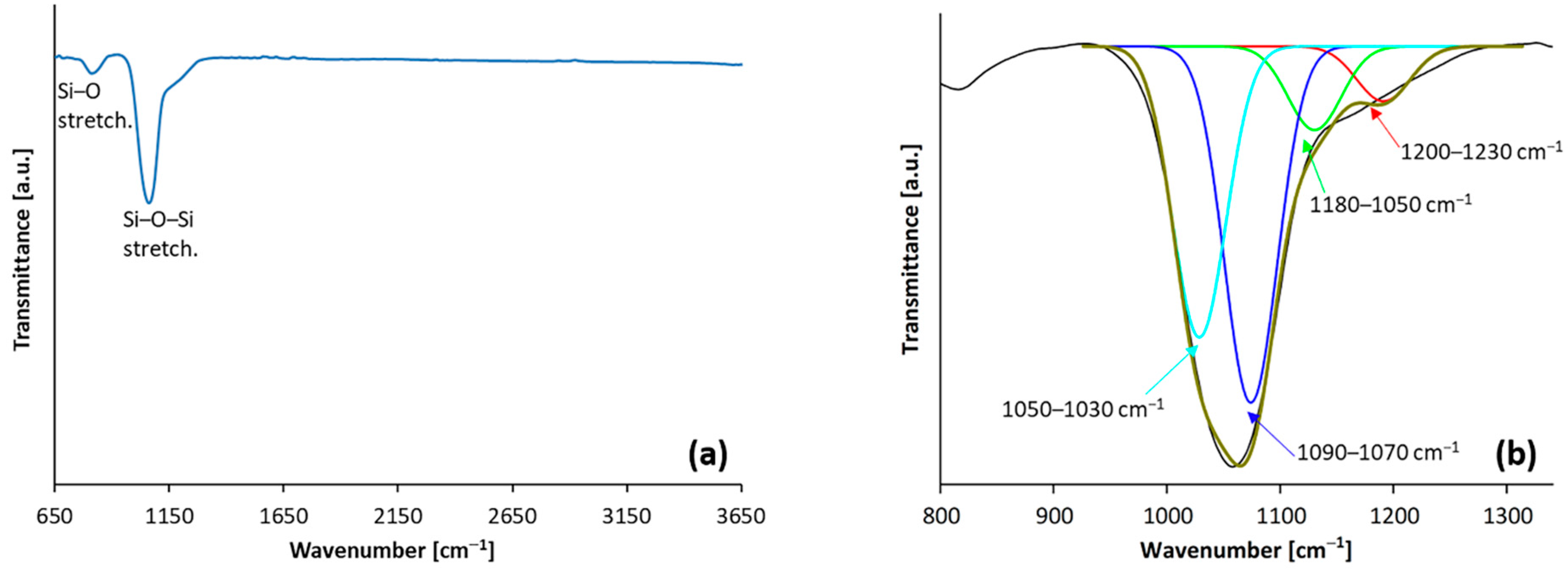
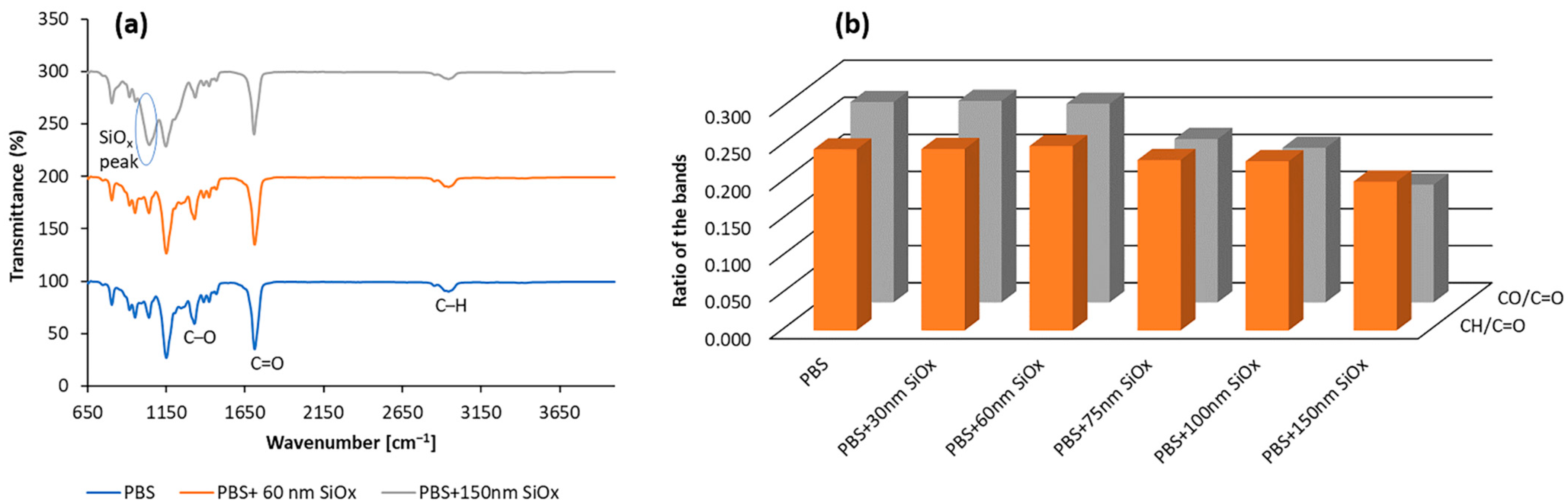
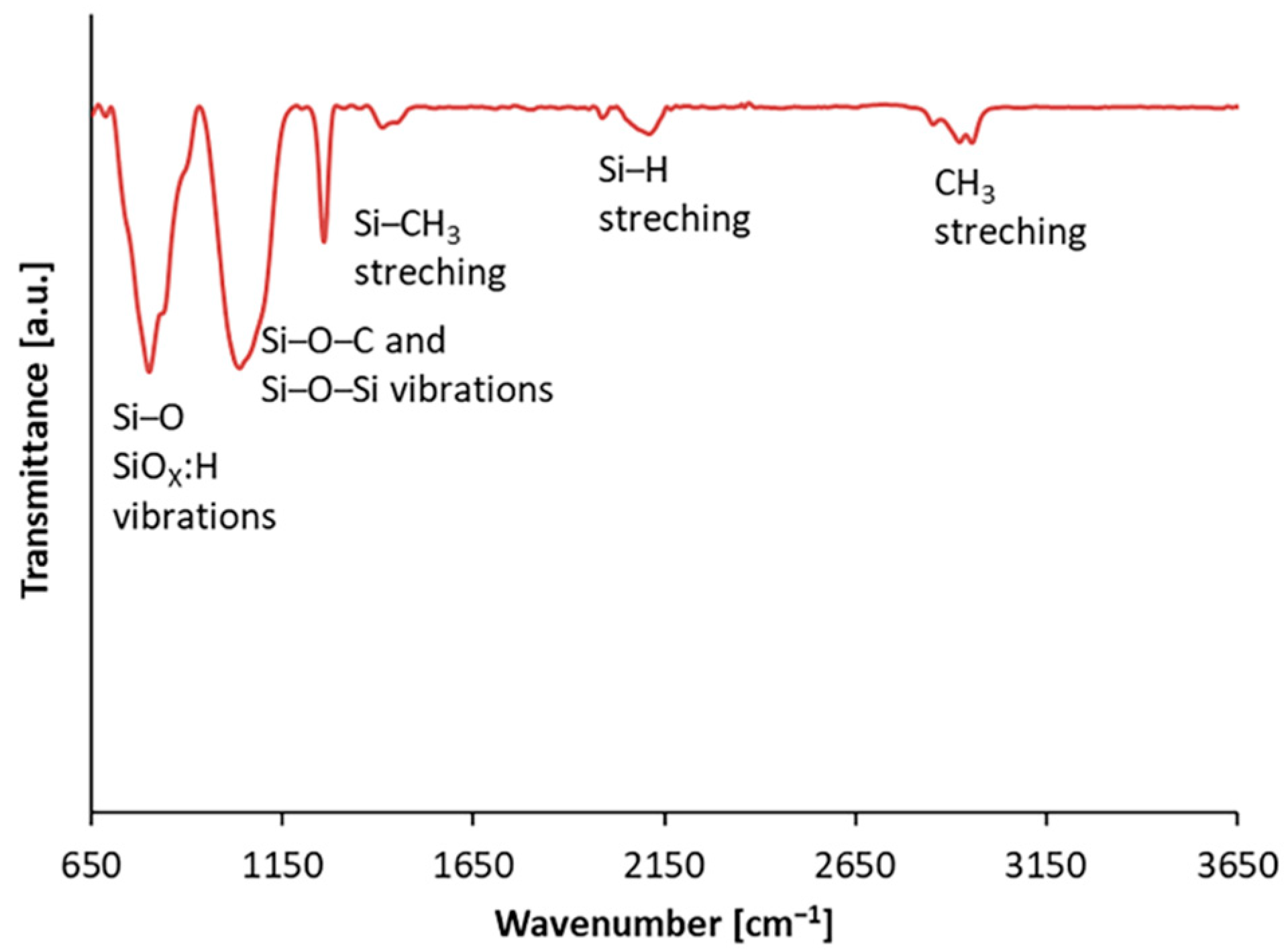
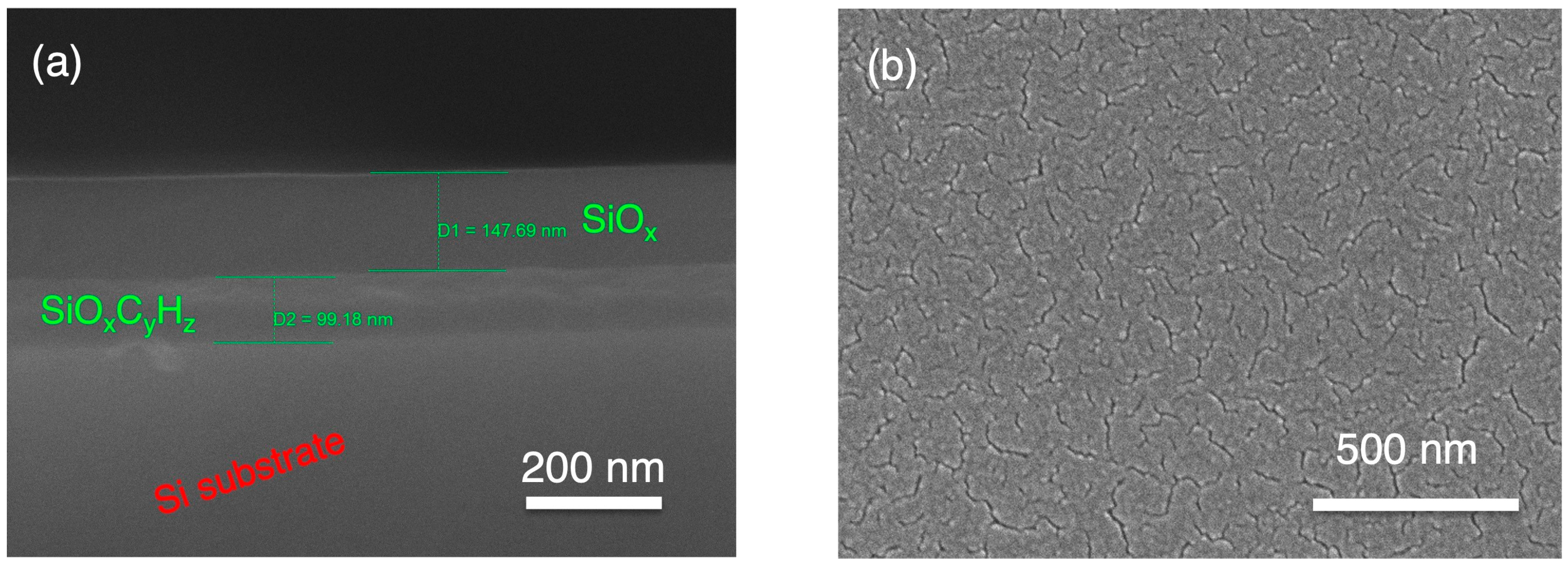
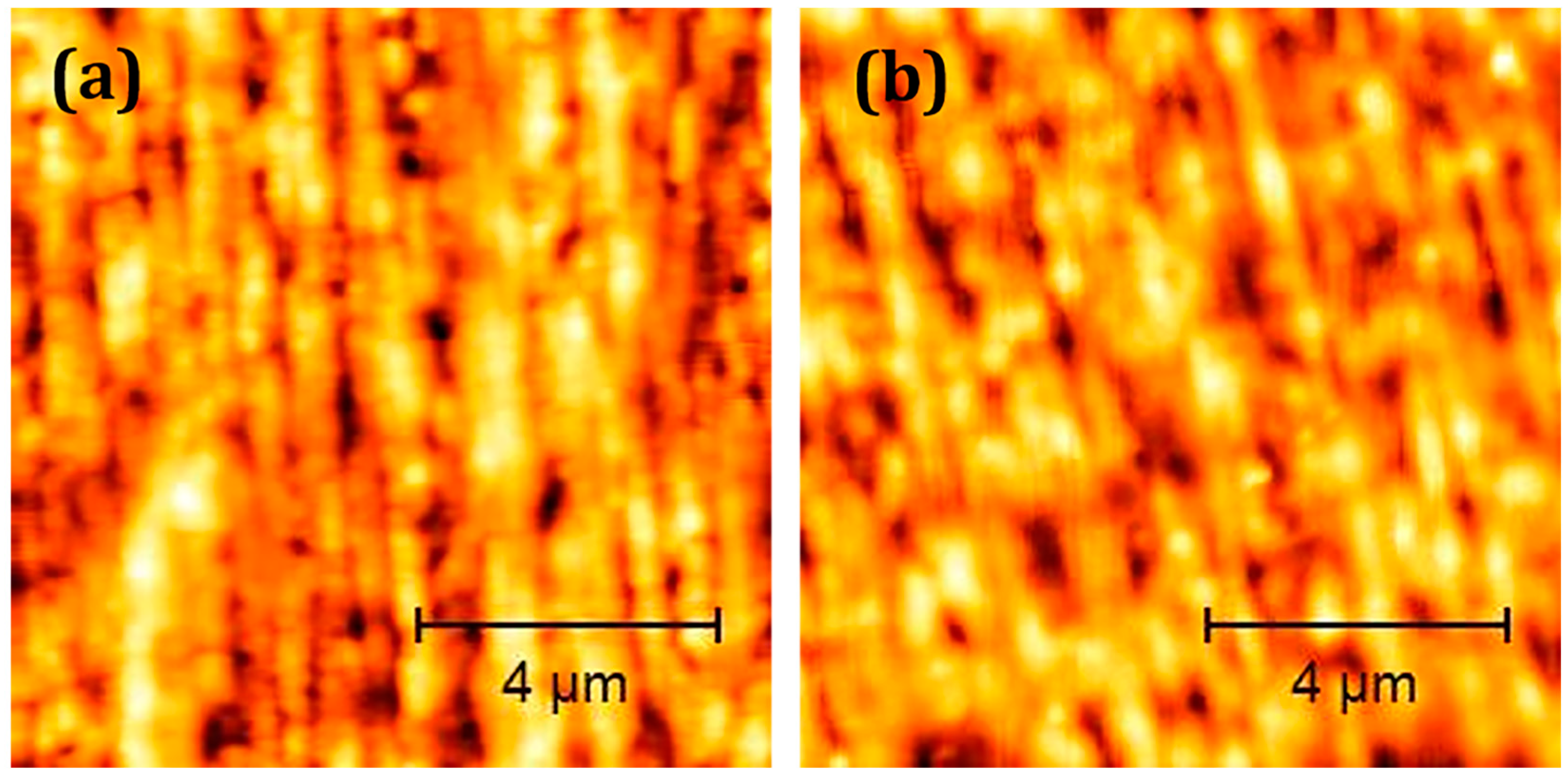
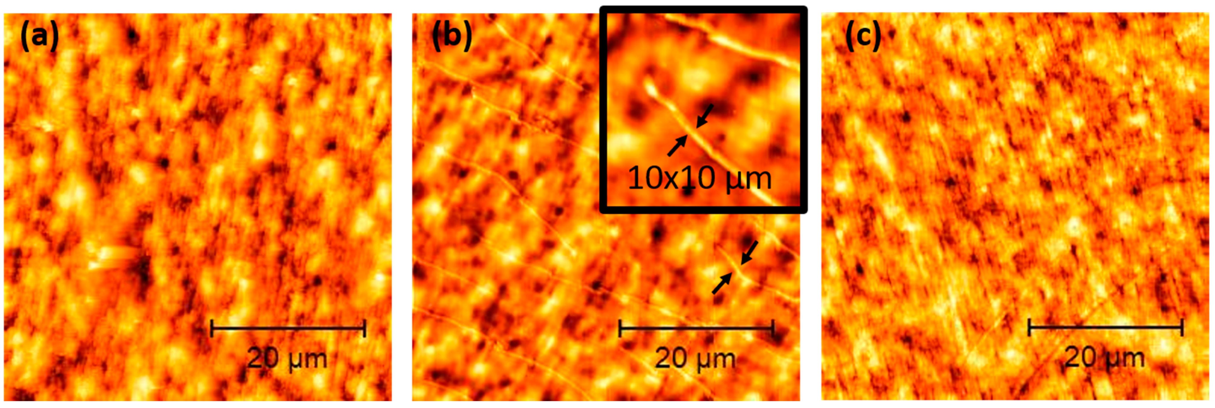
3.1. Characterisation of Coatings

In this study, a transparent organic/inorganic bi-layered film deposited from the same precursor, with or without an admixture of oxygen to the plasma process, was optimised as indicated in Section 2.1. The organic coating, deposited directly onto the polymer, acted as a buffer layer due to the Si–O–C or Si–C groups formed in the coating (see IR analysis), which provided good adhesion between the inorganic top layer and polymeric substrate based on the strong interfacial chemical bonding [8]. Figure 1 shows an example of baseline-corrected IR transmittance of an organic coating (about 100 nm thick, deposition rate = 70 nm/min), which presented high C and H contents due to the incomplete dissociation of the precursor. The IR spectrum showed significant absorption bands from 650 cm−1 to 1300 cm−1 which are connected with SiOx:H, Si−O−C, and Si−O−Si vibrations [32,33,34,35]. In particular, the Si-H stretching and bending absorptions in the SiOx:H groups appear over the 2000–2300 cm−1 and 650–900 cm−1 range, respectively. Regarding the Si–O–Si group, the asymmetric stretching and bending modes were identified at around 1200 and 800 cm−1, respectively. The adsorption bands at 2970 and 1260 cm−1, relative to the stretching of CH3 and the bending modes of methyl groups in Si-(CH3)x, marked the presence of organic components in the film. Medium absorptions at around 840 cm−1 can probably be related to CH3 rocking in Si-CH3. As expected, signals related to organic components disappeared (Figure 2a) in the inorganic coating (about 100 nm thick, deposition rate = 30 nm/min) due to the strong dissociation and reaction of the precursor with the oxygen. In fact, only the characteristic absorption bands of the Si–O–Si group were evident. Regarding the Si–O–Si band in the 1200–950 cm−1 region, it consisted of overlapping peaks from the distribution of local bond types and bond angles that existed in the microstructure (Figure 2b). In the literature, the Si–O–Si band is mainly deconvoluted into three peaks at around 1180–1050, 1090–1070, and 1050–1030 cm−1. The peak in the range 1180–1050 cm−1 could be attributed to Si–O–Si bonds in a cage structure with a bond angle of approximately 150° [36,37,38], and the peak in the range 1090–1070 cm−1 could be assigned to the stretching of smaller-angle Si–O–Si bonds in a network structure, and the peak in the range 1050–1030 cm−1 could be assigned to stretching of even smaller Si–O–Si bond angles, connected to silicon suboxides [39]. However, the analyses of coatings showed that the best deconvolution was in four peaks. Apart from the three characteristic Si–O–Si peaks, the presence of an additional peak (red) was also visible in the 1200–1230 cm−1 region which could be associated with a stretching vibration of Si–O–Si in a large void [40].
In Figure 3, the high-resolution SEM images of organic/inorganic bi-layered films formed on Si are presented. In order to better appreciate the structure of coatings, Figure 3a shows a thick bi-layer coating (~250 nm). It can be observed from the micrograph in Figure 3a that both the organic and inorganic coatings show a uniform and compact structure. From the morphological point of view, organic/inorganic films look quite similar, though they are chemically different (as shown in IR analysis). A smooth and featureless surface is shown in Figure 3b, except for the structure of the gold overlayer.
When assessing the quality of the coating, the surface topography of the bare polymer should be first analysed in order to determine if any defects depend on the underlying material. Figure 4 shows the AFM image of the uncoated PBS foil (a) and PBS coated by plasma with the optimized organic/inorganic bi-layer barrier coating (b). It seems clear that a homogeneous thin coating follows the morphology of the underlying structure. This finding is also supported by surface roughness measurements that in both samples reveal a mean roughness (Ra) of approximately 30 nm.
EDS peaks (Figure 5) confirm FT-IR analyses. According to the weight fractions of the elements, C, Si, and O can be considered to be major elements present in the organic film, while for the inorganic film only Si and O were detected. Furthermore, considering the chemical structure of conventional polydimethylsiloxane, and disregarding H that is not detected by EDS, structures containing 50% C, 25% O, and 25% Si might be expected, while the organic film formed contains 28% C, 36% O, and 36% Si (Figure 5a). This result of elemental composition can be understood considering that the process that converts the HMDSO monomer into plasma polymer is dominated by radical processes yielding mainly amorphous and more or less cross-linked structures; therefore, the monomer does not undergo conventional chemical polymerisation. The inorganic film contains 67% O and 33% Si (Figure 5b), confirming a SiO2-like structure.
To investigate possible chemical changes in the surface structure of PBS as a result of the deposition process, ATR-FTIR analysis was performed as a function of the inorganic coating thickness (Figure 6a). The PBS chemical structure of the repeat unit is –[O–(CH2)4–O–CO–(CH2)2–CO]N [41]. For untreated PBS, it is possible to observe the well-defined bands at 2945 cm−1 (asymmetric deformational vibrations of –CH2– groups), at 1710 cm−1 (C=O stretching vibrations of ester groups and at 1150 cm−1 (stretching of the –C–O–C– group in the ester linkages). For deposits with thicknesses smaller than 60–70 nm, there are no IR absorption bands related to the SiOx coatings, while for bigger thicknesses (for instance, in the coating with a thickness of 150 nm—Figure 6a) the SiOx peak was evident. The calculation of relative percentages of the bands was performed to determine if any bonds had been modified in the treated samples [42,43]. No new bands appeared (within the resolution limits of the instrument) in the treated samples and the ratio of the bands (C-H/C=O, C-O/C=O) remained constant (Figure 6b) for coating thickness smaller than 60–70 nm. These results indicate qualitatively that no change in the surface structure of PBS was found in that range of thickness. In this experimental work, this thickness range was, therefore, chosen to increase the gas-barrier properties of the PBS polymer (see Section 3.3).

3.2. Strategy to Eliminate the Stress in SiOx Barrier Coatings

The application of SiOx barrier coatings on PBS substrates is limited by the incompatibility of the coating and the substrate material due to a large difference in coefficients of thermal expansion (CTE). This incompatibility leads to a reduced durability of the coating over time. Figure 7 shows a PBS substrate coated with a SiOx layer (25 nm thickness). AFM analysis performed immediately after the deposition plasma process showed the appearance of wave-like folding of the coating surface (Figure 7b, black arrows). The presence of a wave-like surface structure suggests a coating instability that can lead to cracking over time. In order to eliminate this phenomenon, a buffer layer (SiOxCyHz) was optimised and deposited at the interface of the polymer and the top coating of SiOx. Si–O–C or Si–C groups (see IR analysis) formed in the buffer layer could provide a good adhesion between the PBS substrate and the SiOx layer subsequently deposited. Such a hybrid system (PBS+SiOxCyHz (25 nm thickness) + 25 nm SiOx) showed (Figure 7c) a surface morphology identical to the untreated PBS.

3.3. Oxygen Transmission Rate Measurements

SiOx-deposited PBS substrates were provided for the evaluation of the oxygen gas properties. Figure 8 shows the oxygen permeability of SiOx barrier films (both with and without a buffer layer) deposited on the PBS substrate as a function of the SiOx coating thickness. In general, all measurements revealed that OTR was reduced for PBS substrate covered with a SiOx barrier film. As expected, due to the minimisation of internal stress during the coating growth, the SiOx barrier film with a buffer layer (SiOxCyHz, 25 nm thickness) produces the best performance (OTR decreases to <5 cc/m2∙day, this corresponds to a reduction of 99% compared to bare PBS), also in function of SiOx thickness.
With regard to the SiOx thickness, a further increase in thickness of more than 20–30 nm led to increased oxygen transmission rate (both with and without buffer layer). As outlined above, the deposition of thin oxide coatings on PBS substrates can produce internal stress. The main sources of internal stress are the coating growth (and associated disorder) and the temperature gradients. Generally speaking, two kinds of defects are found in thin oxide films, namely, microdefects and nanodefects. As for the SiOx-coated PBS without a buffer layer, as highlighted in Section 3.2, the deposition of a few nm of SiO showed the presence of a wave-like surface structure which indicated coating instability; therefore, the worsening of OTR values as a function of SiOx thickness is widely expected. Regarding SiOx-coated PBS with a buffer layer, since the SEM and AFM analysis did not reveal any morphological differences in the thicknesses range considered (10–75 nm), the worsening of OTR values (for thickness above 25 nm) could be, at least partially, attributed to the internal stress generated for increasing deposition time [8].

4. Conclusions

The majority of plastic packaging is produced from fossil-based resources [44], resulting in a large environmental impact. A potentially more sustainable alternative is plastic packaging made from bio-based materials [45]. In particular, biodegradable polymers with an improved barrier against gas are set to be one of the most promising and attractive systems for next-generation sustainable packaging. In this study, the PECVD technique to improve the PBS–oxygen barrier property has been used. PBS was coated by PECVD with transparent organic/inorganic bi-layered coatings while varying the thickness of the SiOx top coating. Internal stresses, which can be generated in the top coating/PBS system during deposition, were eliminated using a buffer layer (25 nm of organic coating) between the PBS and SiOx top layer [46,47,48]. From gas barrier measurements, it could be concluded that the SiOx top coating deposited from the HMDSO/O2 mixture on the PBS possesses a very high oxygen gas barrier capability; thus, an optimal top coating thickness range that combines a very low oxygen permeation and negligible effects of residual stress was determined. For this kind of oxide, the optimal coating thickness is of the order of 10–25 nm. From the point of view of process scalability, the small thickness of the coating could allow for industrialisation due to the very low deposition time.

Author Contributions

E.V.: Conceptualization, Supervision, Project Administration, Funding Acquisition, and Writing—Original Draft; M.P.: Conceptualization, Methodology, Writing—Original Draft, Investigation, and Writing—Review and Editing; M.A.: Resources, Investigation, and Review and Editing; H.C.: Resources, Investigation, and Review and Editing; G.F.: Resources, Investigation, and Review and Editing; S.M.P.: Resources, Investigation, and Review and Editing; and D.R.: Resources, Investigation, and Review and Editing. All authors have read and agreed to the published version of the manuscript.

Funding

This research was funded by the sPATIALS3 project (ID 1176485). It was financed by the European Regional Development Fund under the ROP of the Lombardy Region ERDF 2014–2020 -Axis I “Strengthen technological research, development and innovation”—Action 1.b.1.3 “Support for co-operative R&D activities to develop new sustainable technologies, products and services”—Call Hub.

Data Availability Statement

The data presented in this study are available on request from the corresponding author. The data are not publicly available due to privacy.

Conflicts of Interest

The authors declare no conflict of interest.

References

  1. Kääriäinen, T.O.; Maydannik, P.; Cameron, D.C.; Lahtinen, K.; Johansson, P.; Kuusipalo, J. Atomic layer deposition on polymer based flexible packaging materials: Growth characteristics and diffusion barrier properties. Thin Solid Film. 2011, 519, 3146–3154. [Google Scholar] [CrossRef]
  2. Rügner, K.; Reuter, R.; Ellerweg, D.; de los Arcos, T.; von Keudell, A.; Benedikt, J. Insight into the Reaction Scheme of SiO2 Film Deposition at Atmospheric Pressure. Plasma Process. Polym. 2013, 10, 1061–1073. [Google Scholar] [CrossRef]
  3. Saito, K.; Uchiyama, Y.; Abe, K. Preparation of SiO2 thin films using the Cat-CVD method. Thin Solid Film. 2003, 430, 287–291. [Google Scholar] [CrossRef]
  4. Starostin, S.A.; Creatore, M.; Bouwstra, J.B.; van de Sanden, M.C.M.; de Vries, H.W. Towards Roll-to-Roll Deposition of High Quality Moisture Barrier Films on Polymers by Atmospheric Pressure Plasma Assisted Process. Plasma Process. Polym. 2015, 12, 545–554. [Google Scholar] [CrossRef] [Green Version]
  5. Starostin, S.A.; Keuning, W.; Schalken, J.-P.; Creatore, M.; Kessels, W.M.M.; Bouwstra, J.B.; van de Sanden, M.C.M.; de Vries, H.W. Synergy between Plasma-Assisted ALD and Roll-to-Roll Atmospheric Pressure PE-CVD Processing of Moisture Barrier Films on Polymers. Plasma Process. Polym. 2016, 13, 311–315. [Google Scholar] [CrossRef] [Green Version]
  6. Wu, F.; Misra, M.; Amar; Mohanty, K. Challenges and new opportunities on barrier performance of biodegradable polymers for sustainable packaging. Prog. Polym. Sci. 2021, 117, 101395. [Google Scholar] [CrossRef]
  7. Lieberman, M.A.; Lichtenberg, A.J. Principles of Plasma Discharges and Materials Processing, 2nd ed.; Wiley-Interscience: Hoboken, NJ, USA, 2005. [Google Scholar]
  8. Leterrier, Y. Durability of nanosized oxygen-barrier coatings on polymers. Prog. Mater. Sci. 2003, 48, 1–55. [Google Scholar] [CrossRef] [Green Version]
  9. Zhang, J.; Chen, Q.; Zhang, Y.; Liu, F.; Liu, Z. The power source effect on SiOx coating deposition by plasma enhanced chemical vapor deposition. Thin Solid Film. 2009, 517, 3850–3853. [Google Scholar] [CrossRef]
  10. Fahlteich, J.; Fahland, M.; Schönberger, W.; Schiller, N. Permeation barrier properties of thin oxide films on flexible polymer substrates. Thin Solid Film. 2009, 517, 3075–3080. [Google Scholar] [CrossRef]
  11. Fanelli, F.; Lovascio, S.; d’Agostino, R.; Arefi-Khonsari, F.; Fracassi, F. Ar/HMDSO/O2 Fed Atmospheric Pressure DBDs: Thin Film Deposition and GC-MS Investigation of By-Products. Plasma Process. Polym. 2010, 7, 535–543. [Google Scholar] [CrossRef]
  12. Hegemann, D.; Vohrer, U.; Oehr, C.; Riedel, R. Deposition of SiOx films from O2/HMDSO plasmas. Surf. Coat. Technol. 1999, 116–119, 1033–1036. [Google Scholar] [CrossRef]
  13. Lamendola, R.; d’Agostino, R.; Fracassi, F. Thin film deposition from hexamethyldisiloxane fed glow discharges. Plasma Polym 1997, 2, 147–164. [Google Scholar] [CrossRef]
  14. Teshima, K.; Inoue, Y.; Sugimura, H.; Takai, O. Gas barrier properties of silicon oxide films prepared by plasma-enhanced CVD using tetramethoxysilane. Vacuum 2002, 66, 353–357. [Google Scholar] [CrossRef]
  15. Su, B.J.; Youn, J.K.; Choi, Y.S.; Choi, I.S.; Han, J.G. Characterization of silicon oxide gas barrier films with controlling to the ion current density (ion flux) by plasma enhanced chemical vapor deposition. Thin Solid Film. 2010, 518, 6385–6389. [Google Scholar] [CrossRef]
  16. Sobrinho, A.S.d.; Latrèche, M.; Czeremuszkin, G.; Klemberg-Sapieha, J.E.; Wertheimer, M.R. Transparent barrier coatings on polyethylene terephthalate by single- and dual-frequency plasma-enhanced chemical vapor deposition. J. Vac. Sci. Technol. A 1998, 16, 3190. [Google Scholar] [CrossRef]
  17. Welle, F.; Franz, R. SiOx layer as functional barrier in polyethylene terephthalate (PET) bottles against potential contaminants from post-consumer recycled PET. Food Addit. Contam. Part A 2008, 25, 788–794. [Google Scholar] [CrossRef] [PubMed] [Green Version]
  18. Doi, Y.; Kasuya, K.; Abe, H.; Koyama, N.; Shin-ichi, I.; Koichi, T.; Yoshida, Y. Evaluation of biodegradabilities of biosynthetic and chemosynthetic polyesters in river water. Polym. Degrad. Stab. 1996, 51, 281–286. [Google Scholar] [CrossRef]
  19. Agres, L.; Segui, Y.; Delsol, R.; Raynaud, P. 1996 Oxygen barrier efficiency of hexamethyldisiloxane/oxygen plasma deposited coating. J. Appl. Polym. Sci. 2015, 61, 2015–2022. [Google Scholar] [CrossRef]
  20. Roberts, A.P.; Henry, B.M.; Sutton, A.P.; Grovenor, C.R.M.; Briggs, G.A.D.; Miyamoto, T.; Kano, M.; Tsukaharab, Y.; Yanakab, M. Gas permeation in silicon-oxide/polymer (SiOx/PET) barrier films: Role of the oxide lattice, nano-defects and macro-defects. J. Membr. Sci. 2002, 208, 75–88. [Google Scholar] [CrossRef]
  21. Bensaoula, A.; Wolfe, J.C.; Ignatiev, A.; Fong, F.O.; Leung, T.S. Direct-current magnetron deposition of molybdenum and tungsten with rf-substrate bias. J. Vac. Sci. Technol. 1984, A2, 389. [Google Scholar] [CrossRef]
  22. Milella, A.; Creatore, M.; Blauw, M.A.; van de Sanden, M.C.M. Remote Plasma Deposited Silicon Dioxide-Like Film Densification by Means of RF SubstrateBiasing: Film Chemistry and Morphology. Plasma Process. Polym. 2007, 4, 621–628. [Google Scholar] [CrossRef]
  23. Rastogi, R.; Dharmadhikari, V.; Diebold, A. Stress variation with temperature/time and its correlation to film structure and deposition parameters. J. Vac. Sci. Technol. 1991, A9, 2453. [Google Scholar] [CrossRef]
  24. Vassallo, E.; Caniello, R.; Canetti, M.; Dellasega, D.; Passoni, M. Microstructural characterisation of tungsten coatings deposited using plasma sputtering on Si substrates. Thin Solid Film. 2014, 558, 189–193. [Google Scholar] [CrossRef]
  25. Conrads, H.; Schmidt, M. Plasma generation and plasma sources. Plasma Sources Sci. Technol. 2000, 9, 441–454. [Google Scholar] [CrossRef] [Green Version]
  26. Vassallo, E.; Pedroni, M.; Aloisio, M.; Silvetti, T.; Morandi, S.; Brasca, M. Synergistic Action of Reactive Plasma Particles and UV Radiation to Inactivate Staphylococcus Aureus. Coatings 2022, 12, 1105. [Google Scholar] [CrossRef]
  27. Despax, B.; Makasheva, K.; Caquineau, H. Cyclic powder formation during pulsed injection of hexamethyldisiloxanein an axially asymmetric radiofrequency argon discharge. J. Appl. Phys. 2012, 112, 093302. [Google Scholar] [CrossRef]
  28. Ricci, M.; Dorier, J.L.; Hollenstein, C.; Fayet, P. Influence of argon and nitrogen admixture in HMDSO/O2 plasmas onto powder formation. Plasma Process. Polym. 2011, 8, 108–117. [Google Scholar] [CrossRef]
  29. Creatore, M.; Palumbo, F.; d’Agostino, R. Diagnostics and insights on PECVD for gas-barrier coatings. Pure Appl. Chem. 2002, 74, 407–411. [Google Scholar] [CrossRef] [Green Version]
  30. Deilmann, M.; Theiß, S.; Awakowicz, P. Pulsed microwave plasma polymerization of silicon oxide films: Application of efficient permeation barriers on polyethylene terephthalate. Surf. Coat. Technol. 2008, 202, 1911–1917. [Google Scholar] [CrossRef]
  31. Firpo, G.; Setina, J.; Angeli, E.; Repetto, L.; Valbusa, U. High-Vacuum Setup for Permeability and Diffusivity Measurements by Membrane Techniques. Vacuum 2021, 191, 110368. [Google Scholar] [CrossRef]
  32. Lee, S.; Kang, Y.; Jung, S.; Kim, J.; Kim, D. Plasma-Deposited SiOxCyHz Barrier Coatings for Organic Device Encapsulation. Jpn. J. Appl. Phys. 2013, 52, 076001. [Google Scholar] [CrossRef]
  33. Cech, V.; Zemek, J.; Perina, V. Chemistry of Plasma-Polymerized Vinyltriethoxysilane Controlled by Deposition Conditions. Plasma Process. Polym. 2008, 5, 745–752. [Google Scholar] [CrossRef]
  34. Benissad, N.; Boisse-Laporte, C.; Vallée, C.; Granier, A.; Goullet, A. Silicon dioxide deposition in a microwave plasma reactor. Surf. Coat. Technol. 1999, 116–119, 868–873. [Google Scholar] [CrossRef]
  35. He, L.N.; Wang, D.M.; Hasegawa, S. A study of plasma-deposited amorphous SiOx:H (0 ≤ x ≤ 2.0) using infrared spectroscopy. J. Non-Cryst. Solids 2000, 261, 67–71. [Google Scholar] [CrossRef]
  36. Loboda, M.J.; Grove, C.M.; Schneider, R.F. Properties of a - SiOx:  H  Thin Films Deposited from Hydrogen Silsesquioxane Resins. J. Electrochem. Soc. 1998, 145, 2861–2866. [Google Scholar] [CrossRef]
  37. Albrecht, M.G.; Blanchette, C. Materials Issues with Thin Film Hydrogen Silsesquioxane Low K Dielectric. J. Electrochem. Soc. 1998, 145, 4019. [Google Scholar] [CrossRef]
  38. Lee, L.H.; Chen, W.C.; Liu, W.C. Structural control of oligomeric methyl silsesquioxane precursors and their thin-film properties. J. Polym. Sci. Part A Polym. Chem. 2002, 40, 1560–1571. [Google Scholar] [CrossRef]
  39. Kim, Y.H.; Hwang, M.S.; Kim, H.J.; Kim, J.Y.; Lee, Y. Infrared spectroscopy study of low-dielectric-constant fluorine-incorporated and carbon-incorporated silicon oxide films. J. Appl. Phys. 2001, 90, 3367–3370. [Google Scholar] [CrossRef]
  40. Chou, J.; Lee, S. Effect of porosity on infrared-absorption spectra of silicon dioxide. J. Appl. Phys. 1995, 77, 1805–1807. [Google Scholar] [CrossRef]
  41. Tokiwa, Y.; Calabia, B.; Ugwu, C.; Aiba, S. Biodegradability of plastics. Int. J. Mol. Sci. 2009, 10, 3722–3742. [Google Scholar] [CrossRef] [Green Version]
  42. Moliner, C.; Finocchio, E.; Arato, E.; Ramis, G.; Lagazzo, A. Influence of the Degradation Medium on Water Uptake, Morphology, and Chemical Structure of Poly(Lactic Acid)-Sisal Bio-Composites. Materials 2020, 13, 3974. [Google Scholar] [CrossRef]
  43. Jasmine, A.; Piriya, S.; Wenzel, M.N.; Hill, G.; Wallis, C. Determination of the carbonyl index of polyethylene and polypropylene using specified area under band methodology with ATR-FTIR spectroscopy. E-Polym. 2020, 20, 369–381. [Google Scholar] [CrossRef]
  44. Spierling, S.; Knüpffer, E.; Behnsen, H.; Mudersbach, M.; Krieg, H.; Springer, S.; Albrecht, S.; Hermann, C.; Endres, H.J. Bio-based plastics-a review of environmental, social and economic impact assessments. J. Clean. Prod. 2018, 185, 476–491. [Google Scholar] [CrossRef]
  45. Philp, J.C.; Bartsev, A.; Ritchie, R.J.; Baucher, M.A.; Guy, K. Bioplastics science from a policy vantage point. New Biotechnol. 2013, 30, 635–646. [Google Scholar] [CrossRef] [PubMed]
  46. Abadias, G.; Chason, E.; Keckes, J.; Sebastiani, M.; Thompson, G.B.; Barthel, E.; Doll, G.L.; Murray, C.E.; Stossel, C.H.; Martinu, L. Review Article: Stress in thin films and coatings: Current status, challenges, and prospects. J. Vac. Sci. Technol. A 2018, 36, 020801. [Google Scholar] [CrossRef] [Green Version]
  47. Yu, Z.; Zhao, J.; Xia, F.; Lin, Z.; Zhang, D.; Leng, J.; Xue, W. Enhanced electrical stability of flexible indium tin oxide films prepared on stripe SiO2 buffer layer-coated polymer substrates by magnetron sputtering. Appl. Surf. Sci. 2011, 257, 4807–4810. [Google Scholar] [CrossRef]
  48. Liu, D.-S.; Wu, C.-Y. Adhesion enhancement of hard coatings deposited on flexible plastic substrates using an interfacial buffer layer. J. Phys. D Appl. Phys. 2010, 43, 175301. [Google Scholar] [CrossRef]
Figure 1. FTIR spectrum obtained for the 100 nm of organic coating deposited on silicon at 100 W, Ar/HMDSO ratio 3:1 and 1 Pa.
Plasma 05 00033 g001
Figure 2. FTIR spectrum obtained for 100 nm of inorganic coating deposited on silicon at 200 W, O2/HMDSO ratio 17:1 and 3 Pa (a) curve-fitting to deconvolve the Si–O–Si stretching region (b).
Plasma 05 00033 g002
Figure 3. SEM cross-section of organic and inorganic layers on silicon (a) and top view of the deposit (b).
Plasma 05 00033 g003
Figure 4. AFM images of (a) untreated PBS, (b) PBS coated with a SiOxCyHz (25 nm thickness) + SiOx (25 nm thickness)).
Plasma 05 00033 g004
Figure 5. EDS results, (a) organic and (b) inorganic coating.
Plasma 05 00033 g005
Figure 6. (a) FTIR spectra of untreated and SiOx-coated PBS and (b) I2945/I1710 and I1150/I1710 intensity ratios evaluated as an integrated area for untreated and SiOx-coated PBS.
Plasma 05 00033 g006
Figure 7. AFM images of (a) untreated PBS, (b) PBS coated with a SiOx layer, and (c) PBS coated with SiOxCyHz (25 nm thickness) + SiOx).
Plasma 05 00033 g007
Figure 8. OTR values for coated PBS samples as a function of SiOx thickness with and without buffer layer. Error bars are related to the standard deviation of a set of three measurements.
Plasma 05 00033 g008
Publisher’s Note: MDPI stays neutral with regard to jurisdictional claims in published maps and institutional affiliations.

