Abstract
Aluminum scandium nitride (Al1−xScxN) is a promising ferroelectric material for non-volatile random-access memory devices and electromechanical sensors. However, adverse effects on polarization from electrical leakage are a significant concern for this material. We observed that the electrical conductivity of Al1−xScxN thin films grown on epitaxial TiN(111) buffered Si(111) follows an Arrhenius-type behavior versus the growth temperature, suggesting that point defect incorporation during growth influences the electronic properties of the film. Photoluminescence intensity shows an inverse correlation with growth temperature, which is consistent with increased non-radiative recombination from point defects. Further characterization using secondary ion mass spectrometry in a focused ion beam/scanning electron microscope shows a correlation between trace Ti concentrations in Al1−xScxN films and the growth temperature, further suggesting that extrinsic dopants or alloying components potentially contribute to the point defect chemistry to influence electrical transport. Investigation of the enthalpy of formation of nitrogen vacancies in Al1−xScxN using density functional theory yields values that are in line with electrical conductivity measurements. Additionally, the dependence of nitrogen-vacancy formation energy on proximity to Sc atoms suggests that variations in the local structure may contribute to the occurrence of point defects, which, in turn, can impact electrical leakage. Furthermore, we have demonstrated ferroelectric behavior through electrical measurements and piezoresponse force microscopy after dc bias poling of films in spite of electrical conductivity spanning several orders of magnitude. Although electrical leakage remains a challenge in Al1−xScxN, the material holds potential due to tunable electrical conductivity as a semiconducting ferroelectric material.
1. Introduction
Electrical conduction in aluminum nitride (AlN) has been studied since the 1970s [1,2,3,4,5]. In addition to the material’s susceptibility to incorporating trace amounts of oxygen [6,7], intrinsic (nitrogen and aluminum vacancies [8]) and extrinsic point defects (e.g., interstitial carbon) [1,2] can influence electrical conduction. The reported values for electrical conductivity in AlN exhibit significant variation, further complicating the understanding of this phenomenon [2,9]. Because aluminum scandium nitride (Al1−xScxN) based ferroelectric materials are promising for non-volatile switching in neuromorphic computing applications due to their high remanent polarization, wide memory window, and non-toxicity [10,11,12,13,14,15,16], understanding the structural origins of electrical behavior in this material is crucial for mitigating deleterious effects on devices. Typically, electrical leakage in Al1−xScxN is regarded as undesirable and is often attributed to structural defects, including nitrogen vacancies [17,18,19,20,21]. In this study, we systematically investigate the electrical conduction in Al1−xScxN from the point of view that its electrical properties are influenced by point defects incorporated during growth. Point defect incorporation during growth, be it intrinsic, like vacancies or interstitials, or extrinsic, like impurity elements, can originate from either thermodynamic or kinetic processes. For Al1−xScxN films that are sputter deposited at high temperatures and naturally cooled under ultra-high vacuum (UHV) conditions, the cooling rate may be sufficiently high to kinetically preserve higher concentrations of point defects incorporated during growth. Such phenomena are commonly observed in complex oxides, where sputtered materials must undergo slow cooling under a high oxygen partial pressure to prevent oxygen deficiency [22,23]. In addition, vacancies can bind with extrinsic impurities when the interaction is energetically favorable [24,25].
We observe an Arrhenius-type dependence of electrical conductivity in sputtered Al1−xScxN films on the growth temperature, suggesting correlation with equilibrium point defect concentration. Despite significant direct current (DC) electrical leakage, these films demonstrate ferroelectric behavior, indicating that polarization and free charge carriers can behave independently under external electric fields in this material. Ferroelectric behavior was independently characterized using two different experimental methods. The combined structural characterization, optical property measurements, and physics-based simulations support our contention that the presently observed electrical leakage dependence on the Al1−xScxN growth temperature arises from point defects within the material.
2. Materials and Methods
Al1−xScxN thin films on epitaxial TiN(111) buffered Si(111) substrates were grown with UHV reactive sputtering at substrate temperatures ranging from 446 °C to 805 °C. Current–voltage characteristics were obtained from capacitor structures, which were comprised of Si(111)/TiN(111)/Al1−xScxN(0002)/poly-W layers. These structures underwent a comprehensive analysis employing various structural characterization techniques, including X-ray diffraction (XRD), time-of-flight secondary ion mass spectrometry (ToF-SIMS) in a plasma focused ion beam/scanning electron microscope (PFIB/SEM), and X-ray energy dispersive spectroscopy (EDS) in a scanning electron microscope (SEM). In addition, density functional theory (DFT) calculations were used to estimate the formation energies of the relevant point defect for comparison with experimental data. Finally, ferroelectric properties of the Al1−xScxN films were measured using electrical measurements and piezoresponse force microscopy (PFM).
Growth
Si(111) wafers (2”, arsenic (As) doped, 0.001–0.005 Ω cm) were cleaned in repeated cycles of 15.7 M HNO3(aq), deionized water, and 18.4 M HF(aq). Al1−xScxN films were deposited using reactive sputtering in a load-locked UHV system with a base pressure of <5 × 10⁻¹⁰ Torr. The substrate temperature, as measured by a thermocouple, was calibrated using direct optical access infrared pyrometry with the Si emissivity set to 0.68 [10]. Wafers were heated to 805 °C for 30 min prior to growth. Approximately 200 nm thick epitaxial TiN(111) buffer layers were deposited by sputtering an elemental Ti target (99.995%, Kurt Lesker) in the dc mode at 1.4 A gun current while flowing 4.5 sccm N2 (99.999+%, Airgas) at a total pressure of 9.5 mTorr. Following growth of the TiN(111) buffer layer, the sample was cooled to the film growth temperature, which ranged from 805 °C to 446 °C. Al1−xScxN films were deposited by simultaneously sputtering elemental Al (99.9995%, Kurt Lesker) and Sc (99.99%, Matsurf Technologies, St. Paul, MN, USA) targets in the dc mode at 1.2 A and 0.4 A gun currents, respectively, under an input flow of Ar (20 sccm, 99.999%) and N2 (5.5 sccm, 99.999%), resulting in a total pressure of 5.5 mTorr. The resulting Al:Sc ratio is approximately 30:4 (Table S1); we choose this to avoid Sc compositional segregation at higher Sc concentrations [10]. A substrate bias of −100 V was applied during growth of both TiN and Al1−xScxN. After growth, samples were cooled naturally in UHV. Tungsten (W) top electrodes were defined by sputtering at room temperature through a stainless-steel shadow mask with a square array of 500 µm holes (Stencils Unlimited, Tualatin, OR, USA) using an elemental W (99.95%, Kurt Lesker, Jefferson Hills, PA, USA) target under 20.0 sccm Ar (99.999+%, Airgas, Radnor, PA, USA) input flow at a total pressure of 10.0 Torr in a growth system with a base pressure of <1 × 10⁻⁹ Torr.
Property Measurement
Quasi-DC electrical properties of Al1−xScxN films were probed using two electrode measurements taken from the degenerately doped Si substrate to the W top electrode. Current voltage characteristics were obtained using a Keithley 4200A-SCS with the samples mounted on a microprobe station (Nextron, Yongin-si, Gyeonggi-do, Republic of Korea). The substrate voltage was ramped from 0 V to 20 V, then from 20 V to –20 V, and finally from –20 V to 0 V at a 40 mV step size and an approximately 8 ms interval. Limited current auto-ranging was used to accommodate the potential for large changes in material resistivity due to resistive switching and dielectric breakdown. Successive positive and negative 25 kHz triangle pulses (rise/fall time = 10 μs, no delay) were used to measure the polarization–voltage (P–V) responses. Positive-up negative-down (PUND) measurements were performed using trapezoidal pulses with 10 µs rise/fall time, 10 µs pulse duration, and 10 µs delay between pulses.
Defect fluorescence was characterized at room temperature using a home-built confocal microscope. A 532-nm laser at 10 mW power was used to excite the point defects, and a 550 nm long-pass filter suppressed the residual excitation laser. Fluorescence was collected into a single-mode fiber for spatial filtering and then recorded on a photon detector (SPD). The sample was raster-scanned using a piezoelectric stage and galvanometric mirrors to locate defect clusters. Once identified, their photoluminescence spectra were collected with a Princeton Instruments spectrometer covering 500–1000 nm.
Piezoresponse force microscopy (PFM) was performed using a Bruker Dimension Icon atomic force microscope (Bruker, Billerica, MA, USA) (AFM) with a lock-in frequency of 60 kHz and an ac bias drive amplitude of 10 V applied to the sample. Out-of-plane piezoresponse coefficient (d33) was measured through height changes as a function of the AFM tip bias in pristine films. Residual changes to piezoresponse due to ferroelectricity were probed using DC poling experiments, which were performed in the PFM mode by setting the AC bias drive amplitude applied to the sample to 100 mV while applying DC bias values of ±3 V, ±6 V, and ±12 V to the AFM tip separately in different regions of the sample respective to the sample chuck.
Structural Characterization
Time-of-flight secondary ion mass spectrometry (ToF-SIMS) in a ThermoFisher (Hillsboro, OR, USA) Helios Hydra PFIB/SEM was used to measure signal intensity for detection of trace elements in Al1−xScxN films through depth profiling. Xe+, Ar+, and N2+/N+ plasma sources for the ion beam were employed with a 30 kV accelerating voltage in the positive polarity mode, with the N plasma source chosen to reduce the amount of ion beam induced mixing. For the N source, 30 µm horizontal field width and 2.4 nA nominal beam current (2.82–2.97 nA actual) were used; for the Ar source, 30 µm horizontal field width and 2.0 nA nominal beam current (2.91 nA actual) were used; and for the Xe source, 30 µm horizontal field width and 1.0 nA nominal beam current (1.07 nA actual) were used. Actual beam current varied on the order of 0.01 nA during the course of the experiments. ToF-SIMS experiments were conducted under ~9 × 10⁻⁷ Torr vacuum. Bulk composition measurements using X-ray energy dispersive spectroscopy (EDS) in SEM were performed using an FEI Quanta 600F Environmental SEM (FEI, Hillsboro, OR, USA) in high vacuum mode equipped with a Bruker Xflash 6 SDD EDS detector. Structural characterization using XRD was performed using a Panalytical Empyrean diffractometer with a χ-φ-x-y-z stage using Cu Kα1 radiation (λ = 1.540598 Å) selected through a 4-bounce Ge(220) monochromator. Symmetric θ/2θ, asymmetric φ, and ω rocking curve scans were collected using a PIXcel-3D detector (Malvern Panalytical, Almelo, The Netherlands).
Theory and Calculations
The vacancy formation energy for crystalline AlN and Al1−xScxN systems with charge state was calculated using the equation [26,27],
In Equation (1), is the total energy of the system with one nitrogen vacancy in the charge state . Note that here is the multiple of the charge quantum (e.g., ) and is unitless. represents the energy of the corresponding bulk nitride without vacancies, is the chemical potential of nitrogen in the bulk system, is the valance band maximum energy of the bulk system, and is the electron chemical potential. The value of for the system is not fixed and depends on the chemical environment. Thus, in our calculations we have taken the value of in the range from the valance band maximum (VBM) to the conduction band minimum (CBM). The chemical potential of nitrogen, , is calculated using the relation [28]:
where is the chemical potential of nitrogen in a reference state taken to be solid hcp nitrogen, which is the ground state at 0 K, is the enthalpy of formation of the bulk crystalline nitride without vacancies, and the parameter specifies the stoichiometric condition such that defines the Al-rich condition and defines the N-rich condition. We have also calculated the electrostatic potential alignment differences arising from the presence of the vacancy for the charge states q = 0, +1, +2, and +3 and found the effect to be very small (Figure S1 in Supporting Information (SI)).
We have performed DFT calculations in Quantum Espresso [29] using a plane wave-pseudopotential basis set using the Perdew–Burke–Ernzerhof (PBE) exchange correlation functional [30]. Ultrasoft pseudopotentials [31] were used for all atoms (Al, Sc, and N) in the calculations. For all calculations, the plane wave cut-off energy was set at 70 Ry (~952 eV) after optimization, and k-space integrations were performed with a k-mesh of using the Monkhorst-Pack sampling scheme. A sized supercell of pristine wurtzite-type AlN was constructed using the experimental lattice constant a = 3.11 Å [32], and the optimized value of the c/a ratio was found to be 1.62. Using this ratio, the calculated value of c is 5.038 Å, which agrees with the experimental result (4.98 Å) to within a few percent [32]. The supercell contained a total of 32 atoms (16 Al and 16 N). One nitrogen atom was then removed from the system to create a N vacancy. After creating a vacancy, the system was again fully relaxed and the lattice parameter was optimized while fixing the c/a ratio at 1.62. The optimized value of the lattice parameter after introducing the vacancy was found to be a = 3.12 Å. Self-consistent field (scf) calculations were performed for pristine AlN, AlN with one neutral N vacancy, and for AlN with a charged N vacancy with charge states of +1, +2, and +3.
A Sc-containing system was then created by replacing three of the Al atoms in the structure with Sc atoms to form Al13Sc3N16 (Al0.8125Sc0.1875N). Corresponding Sc-containing systems with one neutral vacancy and with one charged vacancy with charge states of +1, +2, and +3 were also made. These systems (pristine Al0.8125Sc0.1875N, Al0.8125Sc0.1875N with one neutral vacancy, and Al0.8125Sc0.1875N with one charged vacancy with charge states +1, +2, and +3) were also relaxed and optimized lattice parameters were used for scf calculations. To investigate the effect of proximity of the nitrogen vacancy to a Sc atom on the formation energy, we constructed a larger Sc-alloyed AlN (Al0.79Sc0.21N) supercells having 48 (2 × 2 × 3) atoms. Two configurations were considered: one in which the nitrogen vacancy is located close to a Sc atom, and another where the vacancy is positioned farther away. Each system with and without a nitrogen vacancy was relaxed and optimized parameters were used for scf calculations. The scf calculations were run for neutral as well as charged vacancies with charge states +1, +2, and +3 for both systems.
3. Results
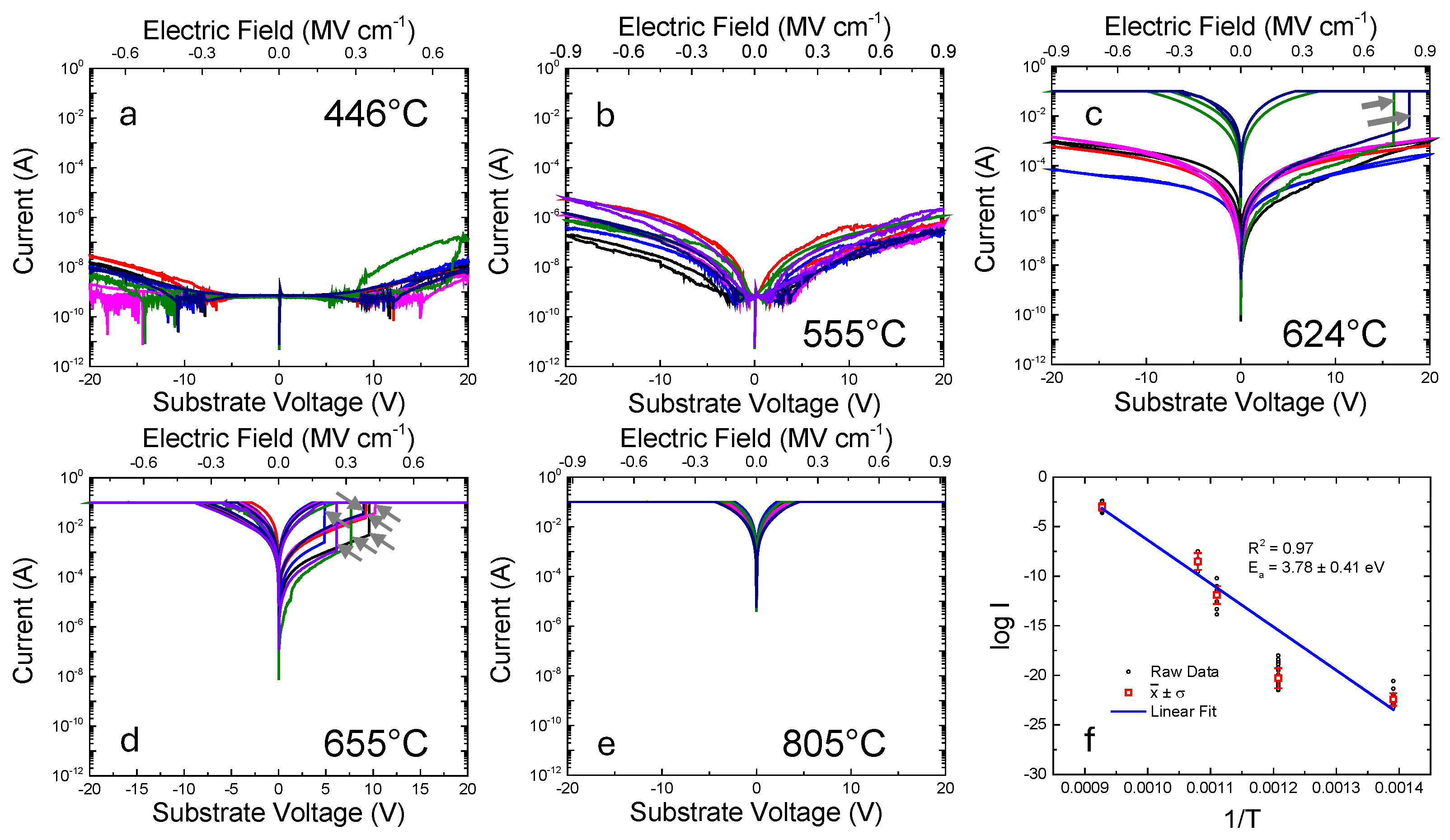
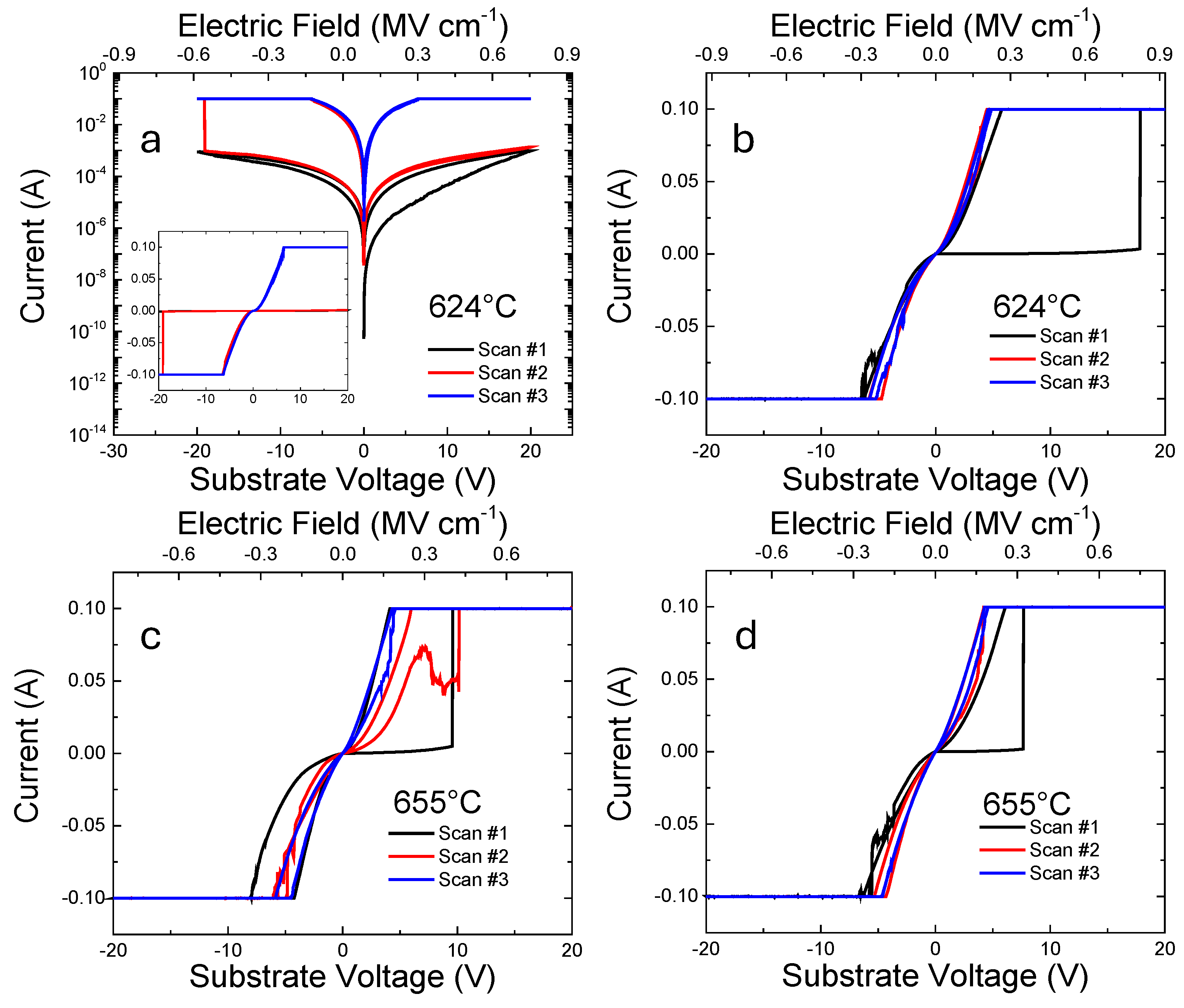
Figure 1a–e illustrate the current–voltage characteristics of multiple devices, each composed of one ~200–300 nm thick Al1−xScxN film deposited at different temperatures on an epitaxial TiN(111) buffer layer on Si(111). While there is some variability in the electrical behavior observed among different devices under the same growth conditions (Figure 1a,b,e), it is notable that the electrical conductivity remains relatively consistent, differing by no more than one order of magnitude for growth temperatures of 446 °C, 555 °C, and 805 °C. We hypothesize that device-to-device variation is influenced by differences in spatial distribution of point defects in the Al1−xScxN films. For growth temperatures of 624 °C and 655 °C, several devices exhibit an irreversible increase in current beyond a certain threshold voltage. In Figure 1f, the current at 2 V (or an equivalent current for the film grown at 446 °C, where the current at 2 V is too low, so the current at 10 V divided by 5 is used instead) is plotted on a logarithmic scale against the inverse of the growth temperature. Fitting the data using an Arrhenius law yields an apparent activation energy of 3.78 eV, with a correlation coefficient of R2 = 0.97. The significant increase in conductivity observed in some devices made from Al1−xScxN films grown at 624 °C and 655 °C is consistent with dielectric breakdown. Figure 2 shows typical current–voltage characteristics from two devices grown at each of these two temperatures. The threshold voltage at which the current exhibits a substantial increase is likely to correspond to the breakdown voltage. Notably, the film grown at 624 °C exhibits a significantly higher breakdown voltage compared to the one grown at 655 °C. These data indicate that Al1−xScxN films with lower electrical conductivity tend to exhibit higher breakdown voltages.
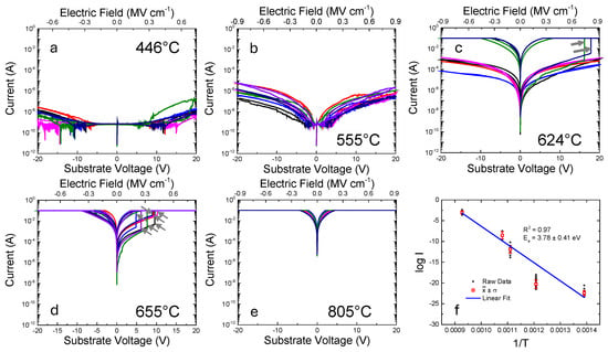
Figure 1.
Current voltage characteristics (multiple devices) of AlScN films grown on epitaxial TiN(111) buffered Si(111) at growth temperatures of (a) 446 °C, (b) 555 °C, (c) 624 °C, (d) 655 °C, and (e) 805 °C and (f) log plot of current at 2 V for T ≥ 555 °C and current at 10 V divided by 5 at T = 446 °C. Gray arrows mark irreversible increases in current due to dielectric breakdown.
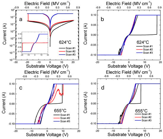
Figure 2.
Current voltage characteristics from two different devices of AlScN films grown at 624 °C (a,b) and from two different devices of AlScN films grown at 655 °C (c,d) showing irreversible increase in electrical conductivity.
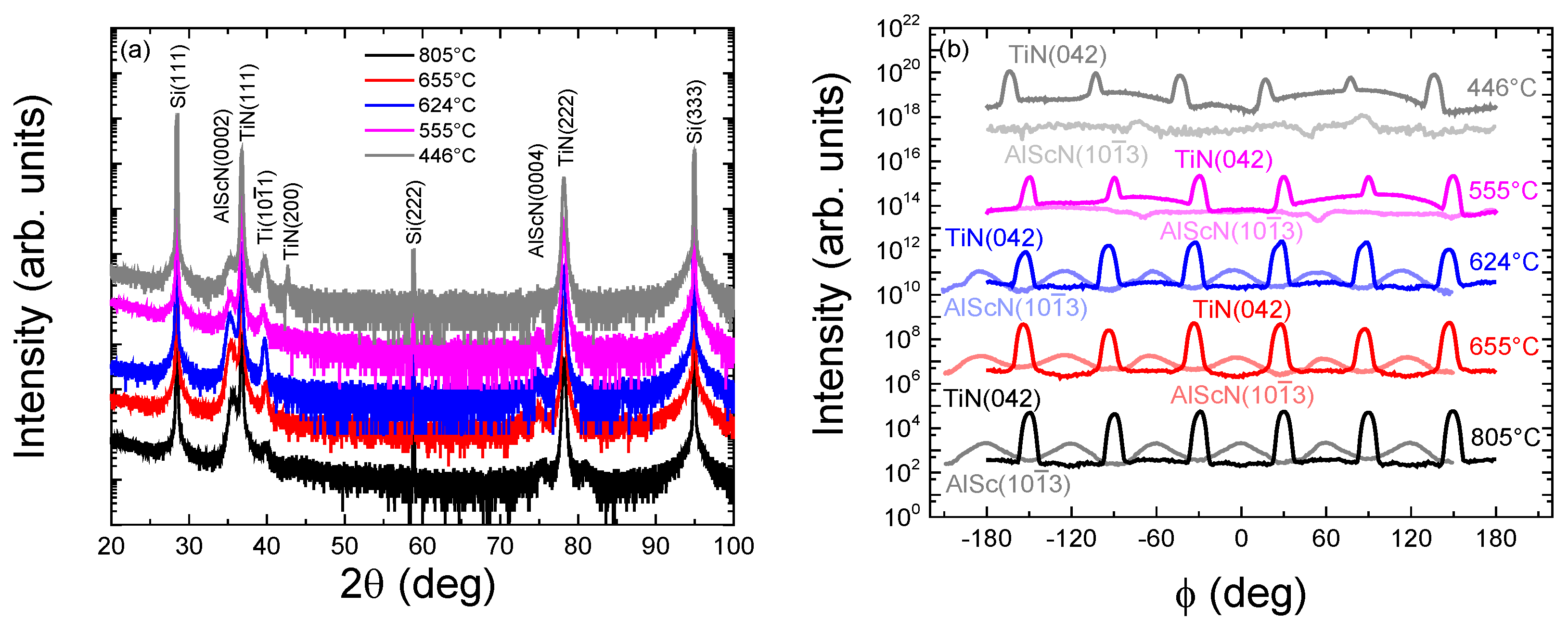
We note that the current–voltage characteristics for Al1−xScxN films grown at 555 °C and higher temperatures differ significantly from reports in the literature as the current increases significantly even for lower applied electric fields < 0.1 MV/cm, independent of dielectric breakdown. The data are consistent with the semiconducting behavior in Al1−xScxN arising from free charge carrier conduction. While electrical leakage can be problematic in ferroelectrics, semiconducting ferroelectrics hold potential for various applications as multifunctional materials [33,34,35]. Structural characterization of the Al1−xScxN films was performed using XRD. Figure 3a,b show symmetric θ/2θ and asymmetric φ scans of Al1−xScxN films on epitaxial TiN(111) buffer layers on Si(111). In the θ/2θ scans, only the Si (111) and TiN (111) family of peaks are observed. In the asymmetric φ scans, six Si (513) peaks and six TiN (042) peaks are observed at the same φ values. This confirms that the TiN buffer layers were grown on Si(111) substrates epitaxially in the cube-on-cube orientation, with TiN(111)∥Si(111) and TiN()∥Si(). Al1−xScxN films grown at temperatures above 600 °C exhibit only the (0002) family of peaks in the θ/2θ scan and show six peaks offset 30° from the TiN (042) peaks in the asymmetric φ scan. These films are, thus, epitaxial with Al1−xScxN(0002)∥TiN(111)∥Si(111) and Al1−xScxN∥TiN()∥Si(). However, for growth temperatures below 600 °C, the asymmetric φ scans show that the in-plane registry of the Al1−xScxN film with respect to the epitaxial TiN buffer layer is lost. This loss of Al1−xScxN epitaxy at growth temperatures below 600 °C is consistent with previous observations on growth of AlN on Si(111) [36]. Reciprocal space maps (RSM) depicting the peaks corresponding to the film (0002) and buffer (111) reflections for different film growth temperatures are shown in Figure S2 of the Supplemental Information (SI) section. Notably, the width of the film peak in the in-plane direction increases as the film growth temperature decreases.
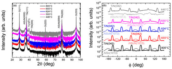
Figure 3.
XRD (a) θ–2θ scans and (b) asymmetric φ scans of AlScN/TiN(111)/Si(111) showing loss of epitaxy for growth temperatures below 624 °C.
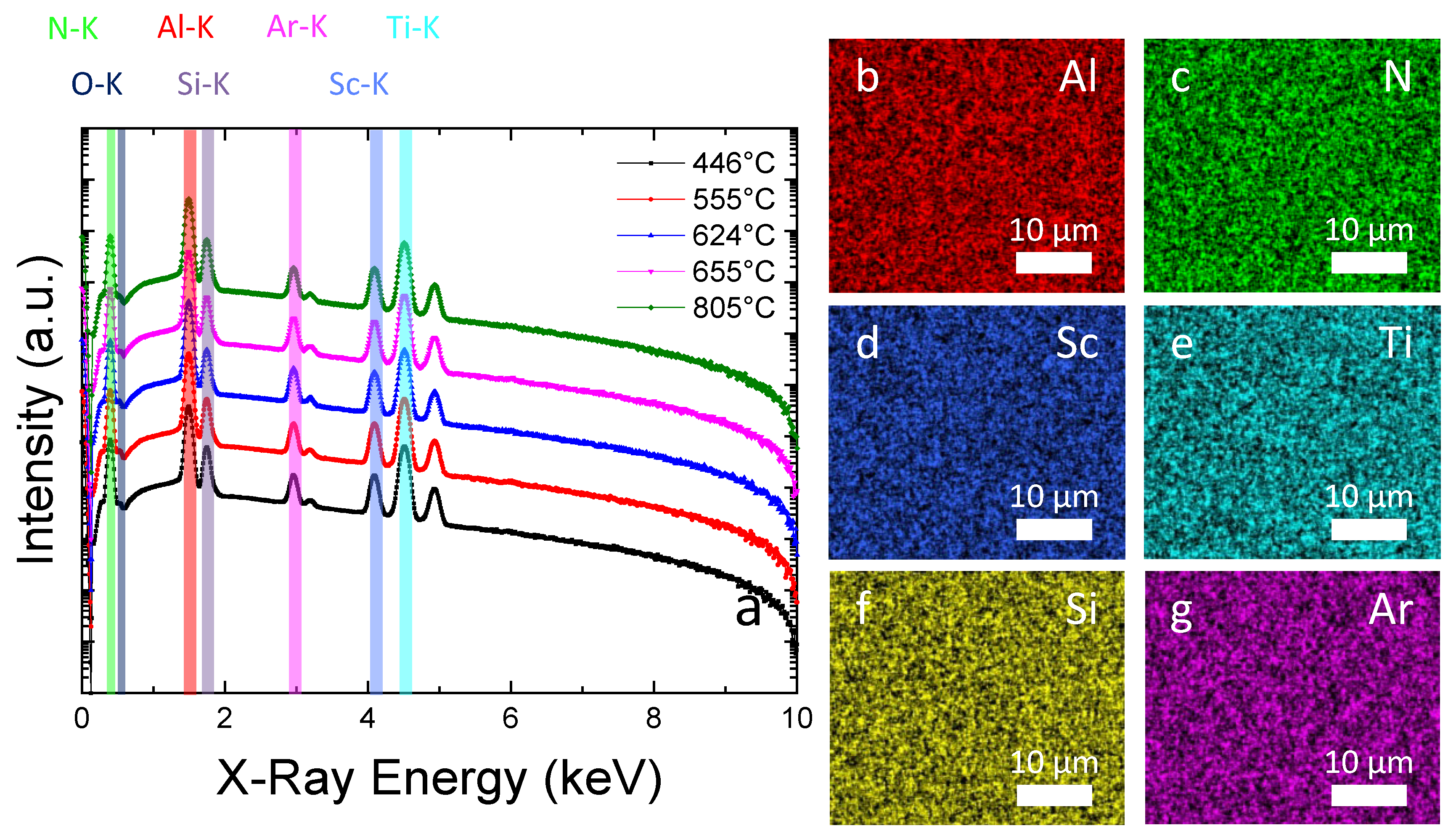
To ascertain the bulk composition of the Al1−xScxN films, SEM-EDS analysis was used. In Figure 4a, spectra from Al1−xScxN films grown at temperatures ranging from 446 °C to 805 °C are presented, and the corresponding compositional data are summarized in Table S1 (in Supporting Information). The results indicate that the primary constituents of the film are aluminum, scandium, and nitrogen, with trace amounts of oxygen also detected. The film compositions exhibit no statistically significant variation with respect to the growth temperature. Due to the interaction volume of the electron beam, a Ti signal from the TiN buffer layer is also present. Through FIB/ToF-SIMS depth profiling (Figure 5a–e) of the capacitor devices, we can discern the layers, including the tungsten (W) top electrode, the Al1−xScxN film, and the TiN buffer layer. Here we note that the ToF-SIMS intensity does not necessarily scale linearly with the concentration due to differences in sputter yield and ionization cross section [37] and cannot be used to quantitatively determine the concentration [38]. Nonetheless, trace element detection and the comparison of relative intensities are possible. In the W layer, there is minimal detection of the Al, Sc, N, Ti, and O signal. The EDS and ToF-SIMS data are consistent in showing the main components of the Al1−xScxN films to be Al, Sc, and N. When the depth profile reaches the top electrode/Al1−xScxN film interface, we observe that Al, Sc, N, Ti, and O signals rise. This indicates that the Al1−xScxN films contain trace Ti and O at a level detectable through ToF-SIMS. Within the Al1−xScxN films grown at 624 °C, 655 °C, and 805 °C, there are small variations in the signal intensity that may stem from minor fluctuations in ion beam current, local variations in the sputter yield of the film, or uneven re-sputtering at the edge of the ion beam milled crater. Finally, we observe that the Ti:(Al+Sc) intensity ratio within the film at a fixed distance from the top electrode/film interface exhibits an approximately linear increase as a function of Al1−xScxN film growth temperature (Figure 5f). The integrated mass spectra corresponding to Figure 5a–e are shown in Figure S3. Projected top view (Figure S4) and side view (Figure S5) images of the ToF-SIMS data are also shown in the Supporting Information section.

Figure 4.
(a) SEM-EDS spectra of AlScN films grown on epitaxial TiN(111) buffered Si(111) at different growth temperatures and corresponding color-coded SEM-EDS maps of the 446 °C growth showing (b) Al, (c) N, (d) Sc, (e) Ti, (f) Si, and (g) Ar signal intensities.
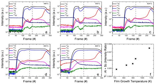
Figure 5.
FIB ToF-SIMS depth profiles of AlScN films grown on epitaxial TiN(111) buffered Si(111) at growth temperatures of (a) 446 °C, (b) 555 °C, (c) 624 °C, (d) 655 °C, and (e) 805 °C and (f) intensity ratio of Ti:(Al+Sc) signals at the dotted line in the depth profiles (a–e) as a function of growth temperature. The traces for the signals are as follows: 27Al (black), 48Ti (red), 45Sc (blue), 14N (magenta), 16O (green), and 183W (navy).
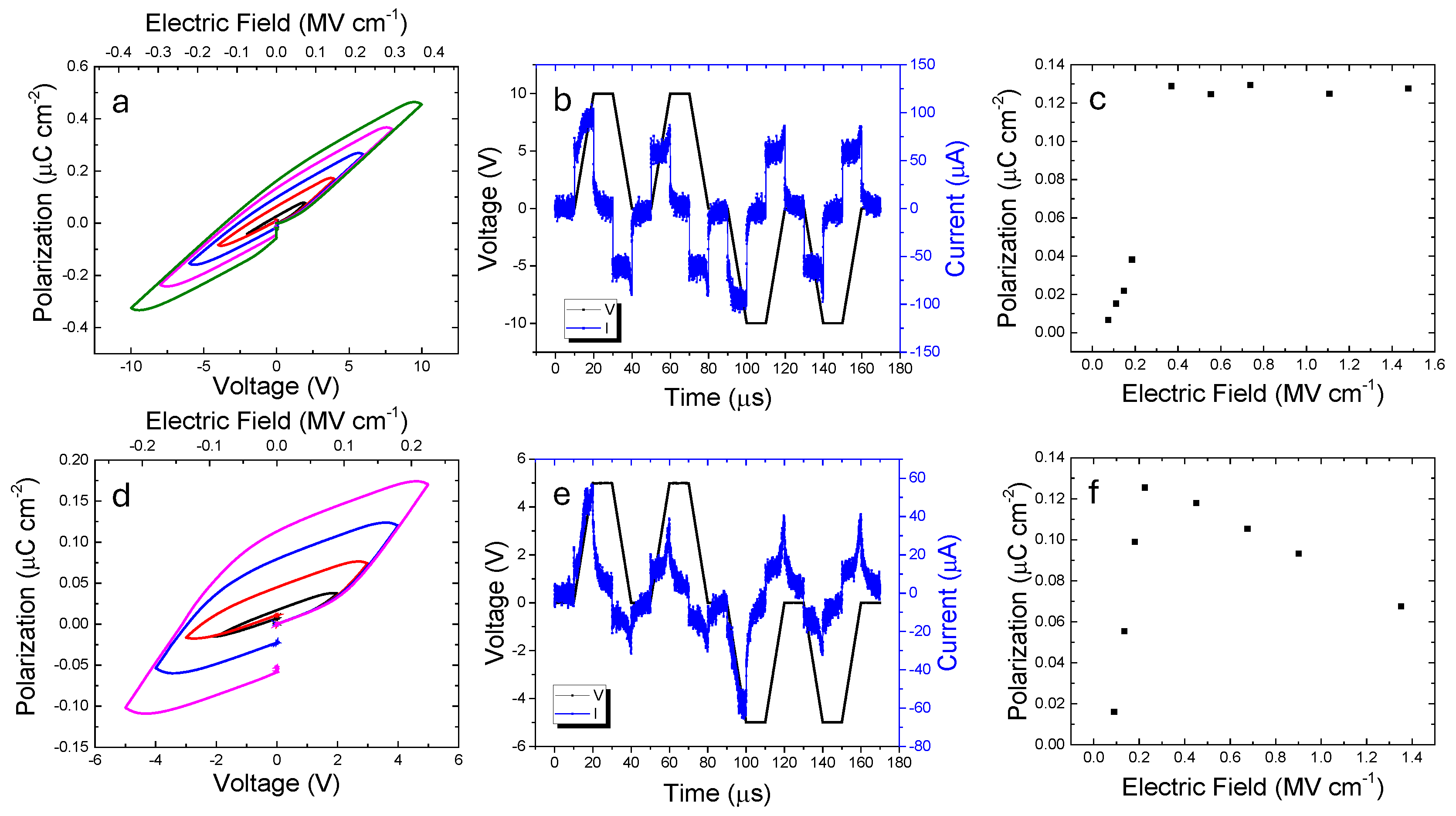
The ferroelectric properties of the Al1−xScxN thin films were characterized using both polarization-electric field hysteresis and positive-up negative-down (PUND) measurements (Figure 6). These measurements were only performed on Al1−xScxN grown at 446 °C and 555 °C because films grown at higher temperatures exhibited significant electrical leakage, impeding the measurement. Both of these films exhibit a remanent polarization (Pr)~0.13 μC cm−2 (Figure 6a,c,d,f), which is significantly lower than what is reported for Al1−xScxN [39]. There are several potential factors contributing to the low Pr. First, the Sc composition of Al1−xScxN films in the current study are not optimized as the focus is on the origins of electrical leakage. Previously we found compositional segregation consistent with spinodal decomposition for Sc compositions above 20 at%, so, for this study, we chose a Sc composition below this value to avoid possible complications related to phase separation [10]. Second, an electrical leakage induced IR drop in the ferroelectric properties can decrease the effective electric field in the material and, therefore, the Pr. Finally, the electrical leakage increases significantly when the applied electric field approaches 0.2–0.3 MV/cm, at which point the polarization saturates; on the other hand, some works report higher coercive fields~2–4 MV/cm [39]. The relationship between the onset electric field for increased electrical leakage and the electrical breakdown point may play a role. For the current study, even though the samples grown at 446 °C and 555 °C do not undergo dielectric breakdown up to 0.8 MV/cm, the electrical leakage onset is significantly lower (~0.3 MV/cm). However, we demonstrate that there is a ferroelectric response even in the presence of significant electrical leakage, indicating that Al1−xScxN is potentially a semiconducting ferroelectric material. The PUND measurements at saturation show comparable leakage currents for Al1−xScxN grown at 446 °C and 555 °C; remanent polarization of the 555 °C samples begins to decrease after saturation. This indicates that the leakage current increases faster than the polarization current beyond a threshold voltage for the higher temperature growth. These results are also consistent with the electrical leakage results, showing that increased growth temperature lowers the breakdown voltage.
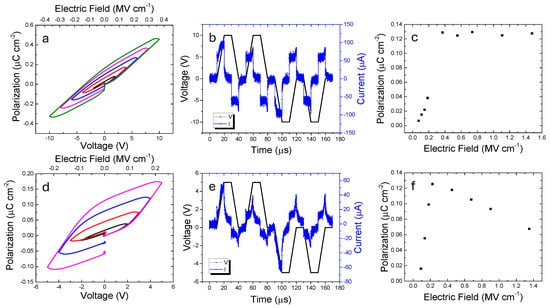
Figure 6.
Ferroelectric properties of AlScN on TiN buffered Si(111) grown at 446 °C: (a) P–E hysteresis loops, (b) PUND measurement, and (c) remanent polarization, as measured by PUND, as a function of applied electric field and ferroelectric properties of AlScN on TiN buffered Si(111) grown at 555 °C: (d) P–E hysteresis loops, (e) PUND measurement, and (f) remanent polarization, as measured by PUND, as a function of applied electric field.
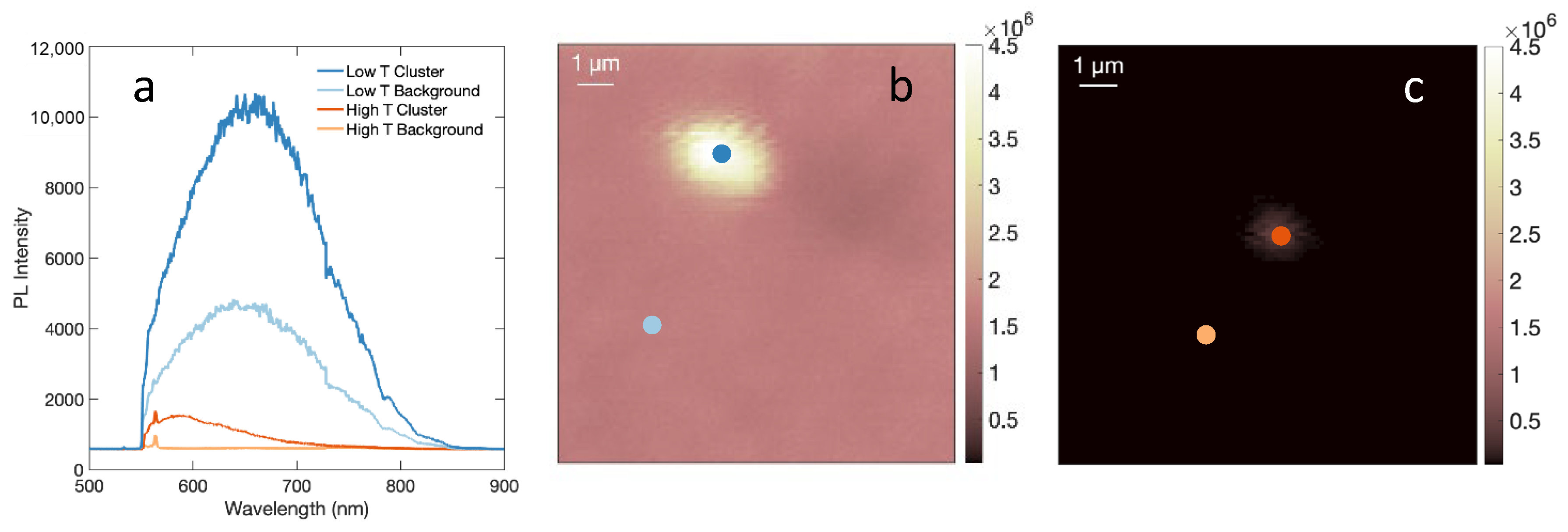
Room temperature photoluminescence (PL) was measured on Al1−xScxN grown both with inductively coupled plasma (ICP) assist in the absence of substrate heating and at 805 °C without ICP assist (Figure 7a). Both samples exhibit broad emission that is peaked at wavelengths between 600 nm and 700 nm. This is consistent with radiative recombination from oxygen substitutional defects [40,41]. Furthermore, the two samples exhibit similar oxygen concentrations, as indicated through EDS (Figure 4) and ToF-SIMS (Figure 5). Photoluminescence imaging of the two samples shows similar features: bright emission from small clusters and weaker emission from the surrounding field regions. In both the clusters and the surrounding field regions, the PL intensity of Al1−xScxN grown at higher temperature is significantly lower than that of Al1−xScxN grown at lower temperature. Because trace oxygen content in the two samples is very similar, the difference in PL intensity indicates increased non-radiative recombination in the Al1−xScxN grown at higher temperature. This is consistent with increased point defect concentration, which can result in higher rates of Shockley–Read–Hall recombination through trap-assisted non-radiative processes [42,43,44].
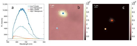
Figure 7.
Photoluminescence spectra (a) from cluster and field regions of the sample for low temperature and high temperature AlScN growths and photoluminescence imaging showing bright emission from small clusters on AlScN grown at (b) low temperature and (c) high temperature. PL spectra from (a) are collected from the regions marked by the corresponding color-coded dots in (b) and (c).
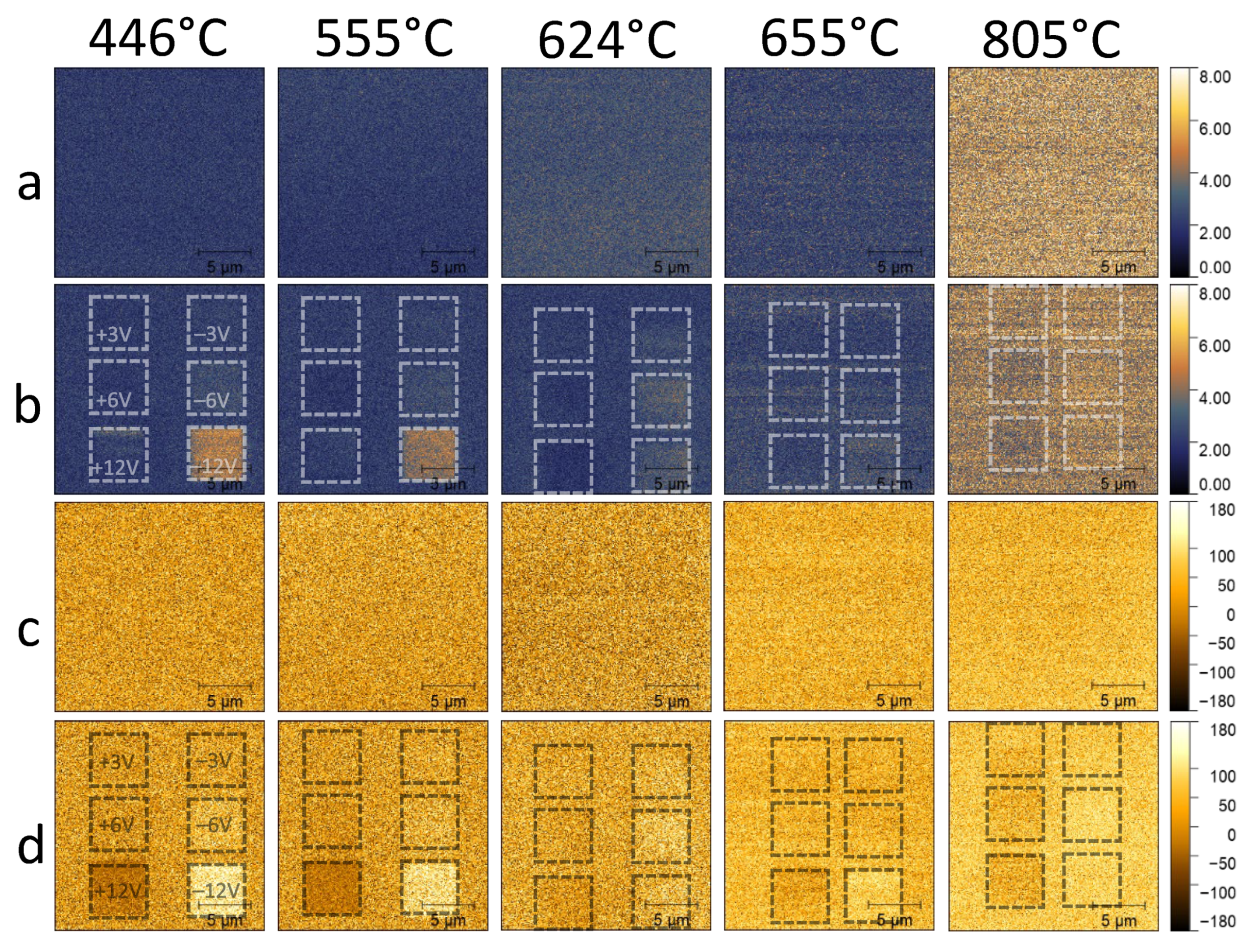
Ferroelectric behavior was also confirmed through DC poling PFM experiments. The piezoresponse amplitude and phase of the pristine sample (Figure 8a and Figure 8c, respectively) and of the same area of the sample after poling at ±3 V, ±6 V, and ±12 V (Figure 8b and Figure 8d, respectively) are consistent with changes in piezoresponse due to ferroelectricity, although we note that this response can also arise from ionic conductivity. Opposite signs of the piezoresponse phase are observed for positive and negative DC poling voltages, as expected for a ferroelectric material. Also, the change in the piezoresponse amplitude and phase is more apparent in the films grown at lower temperatures (446 °C and 555 °C). This is primarily because these samples exhibited less electrical leakage, resulting in a higher ratio of the polarization current to the shunting current, which, in turn, manifests as an increased piezoresponse. Figure 8 shows piezoresponse measured in low voltage mode, in which the maximum tip bias in the AFM is ±12 V, limiting the electric field in the Al1−xScxN to ~1.2 MV cm−1 without considering shunting currents, which is slightly lower than the reported coercive field of Al1−xScxN [39]. High voltage poling data was also collected (DC bias: ±15 V, ±30 V); details are provided in the Supporting Information (Supporting Information, Figure S6).
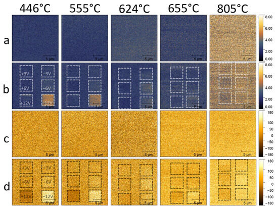
Figure 8.
Piezoresponse amplitude (mV) of (a) pristine AlScN films grown at different temperatures and (b) the same regions of the samples in (a) after dc bias poling at ±3 V, ±6 V, and ±12 V, as indicated by the white dotted rectangles. Piezoresponse phase (deg) of (c) pristine AlScN films grown at different temperatures and (d) the same regions of the samples in (c) after dc bias poling at ±3 V, ±6 V, and ±12 V, as indicated by the black dotted rectangles.
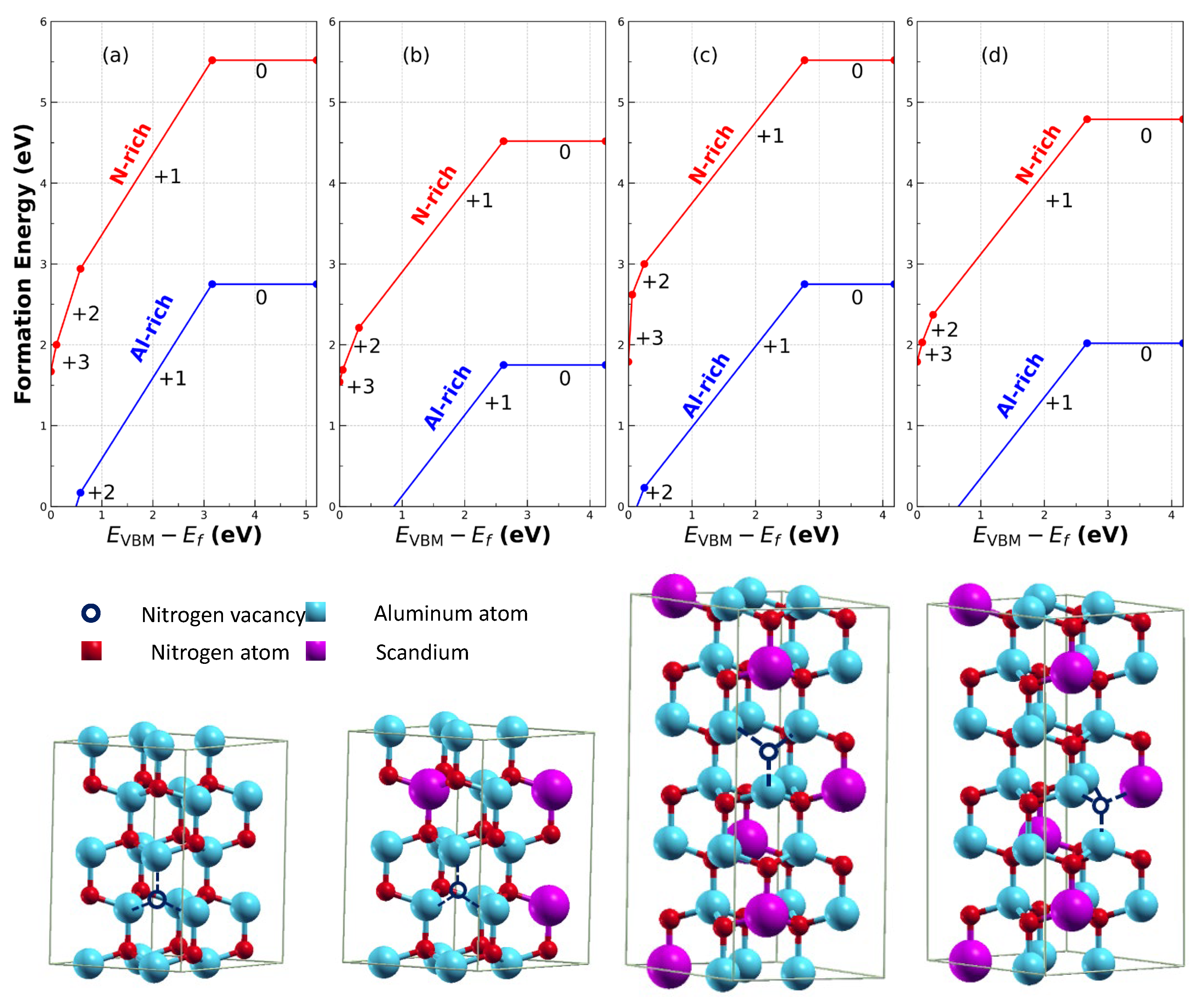
The bandgap energies for pristine AlN and Al0.8125Sc0.1875N were calculated to be 5.21 eV and 4.25 eV, respectively, using the PBE functional. Underestimation of the bandgap in the generalized gradient approximation is well known [45]. The N-vacancy formation energy of AlN and Al0.8125Sc0.1875N as a function of Fermi energy are plotted in Figure 9a,b. In both systems, kink discontinuities arise because the formation energy of a nitrogen vacancy with charge states +3, +2, and +1 decreases as the Fermi energy approaches the valence band maximum (VBM). Increasingly positively charged configurations of the vacancy have a lower formation energy and are energetically preferred closer to the VBM. Furthermore, the N-vacancy formation energy is 2.77 eV lower under Al-rich conditions compared to N-rich conditions. At the VBM, the formation energies for a N-vacancy with +3 charge state are 1.67 eV and 1.54 eV for AlN and Al0.8125Sc0.1875N, respectively, under N-rich conditions. Conversely, the neutral N-vacancy formation energies for pristine AlN and Al0.8125Sc0.1875N are 5.52 and 4.52 eV, respectively, for N-rich conditions. The values of neutral N-vacancy formation energies in pristine AlN for N-rich (5.52 eV) and Al-rich (2.75 eV) conditions are consistent with previous calculations on wurtzite Al1−xScxN [46]. These findings suggest that the formation energy of a N-vacancy in Sc-alloyed AlN is less than in pristine AlN for all charge states, irrespective of whether the system is under N- or Al-rich conditions. Thus, the formation of N vacancies in Al1−xScxN is more energetically favorable than in AlN. Finally, the N-vacancy formation energy in Al0.79Sc0.21N for a nitrogen vacancy with one Sc nearest neighbor and a nitrogen vacancy with no Sc nearest neighbors is shown in Figure 9c and Figure 9d, respectively. The N vacancy with a Sc nearest neighbor exhibits a formation energy nearly 1 eV lower than the N vacancy with no Sc nearest neighbors. This preference can be attributed to the larger size of Sc atoms compared to Al atoms, as vacancies adjacent to Sc atoms help alleviate local strain and are energetically favored.
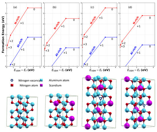
Figure 9.
The nitrogen-vacancy formation energy as a function of Fermi energy on (a) pristine AlN and (b) on Al0.8125Sc0.1875N for nitrogen- and Al-rich conditions and for a slightly larger supercell on Al0.79Sc0.21N when the vacancy has (c) no Sc nearest neighbor atoms and (d) one Sc nearest neighbor atom for N- and Al-rich conditions and (bottom row) atom and vacancy positions for simulations in (a–d).
4. Discussion
One important consideration is the significantly lower than expected value of remanent polarization we measured in the sputtered Al1−xScxN films. First, we emphasize that the remanent polarizations obtained through PUND measurements subtract out all leakage current contributions. To rationalize such low remanent polarization values, we considered a circuit model for a leaky ferroelectric thin film that includes one resistance in series with the ferroelectric material. We saw that the leakage current measured by PUND was approximately 40 µA for a 5 V pulse (Figure 6e), which yields 1.25 × 10⁵ Ω. This is a series resistance because it is obtained from the U (second) pulse of the PUND measurement, which has no contribution from the polarization current. When a voltage is applied to the leaky ferroelectric thin film, the current passing through the series resistance results in a voltage drop that reduces the electric field across the ferroelectric film in a similar way to a voltage divider. Because the leakage current is much larger than the polarization current, a larger fraction of the applied voltage will be dropped across the series resistance than across the ferroelectric film. As a result, the effective electric field across the ferroelectric film could be reduced by more than half. This is consistent with the observation that the observed remanent polarization is significantly muted.
Our results on the dependence of Al1−xScxN electrical properties on the film growth temperature are quite surprising. We observed increased electrical leakage in films with higher crystallinity (lower in-plane peak width in XRD RSM). This runs counter to expectations that films with higher crystallinity should exhibit a stronger ferroelectric response. Observations of point defect signatures (electrical conductivity Arrhenius dependence on growth temperature, SIMS, photoluminescence, and DFT) provide the missing explanation.
The equilibrium vacancy concentration in a crystal governed by thermodynamics follows an Arrhenius law and can be derived by balancing the configurational entropy gained from vacancies with their enthalpy of formation. In the case of Al1−xScxN films, the observed Arrhenius relationship between electrical conductivity and growth temperature indicates an apparent activation energy of 3.78 eV. Using this activation energy to calculate the vacancy concentration in the dilute regime yields a vacancy fraction of approximately 1.7 × 10⁻²⁰ at 805 °C. This may not be the actual vacancy concentration because (1) the vacancies may not fully equilibrate at the growth temperature and (2) the change in vacancy concentration when the film naturally cools to room temperature could be kinetically controlled. Nevertheless, it is worth emphasizing that the range of N-vacancy formation energies calculated by DFT is in the range of several electron volts, which aligns with the observed electrical behavior and suggests a connection between vacancy formation and the electrical properties of the material.
Although we were unable to directly measure vacancy concentrations, several experiments provide supporting evidence for the involvement of nitrogen vacancies in the electrical conduction of Al1−xScxN. First, the observed dielectric breakdown behavior closely resembles previous reports of electrical conduction induced by nitrogen vacancies [47]. Second, bulk composition measurements using STEM-EDS indicate a nitrogen deficiency in the film/buffer/substrate system consistent with the presence of nitrogen vacancies in either the Al1−xScxN film [17,18,19,20,21], the TiN buffer [48], or, potentially, both layers. Finally, the SIMS data indicate an increased Ti concentration in the Al1−xScxN films as a function of growth temperature. We know that the proximity of N vacancies to Sc atoms reduces the vacancy formation energy, which is consistent with an argument based on atomic radius [49]. Assuming the same applies for the presence of trace Ti, which has a similar atomic size to Sc (they are adjacent in the periodic table), the increased Ti concentration can also lead to an increased N-vacancy concentration due to vacancy-impurity binding. We noted that compared to other characterization methods such as EDS, SIMS has a detection threshold that is significantly lower (~1016 cm−3) [50]. Because point defect concentrations are typically very low, this makes SIMS uniquely well suited for their characterization due to the sensitivity of the measurement. Note that while a DFT simulation including trace Ti is possible, the system size required would be too large—therefore, we offer, instead, a conjecture based on a physical argument rooted in atomic size. Collectively, the data are consistent with electrical conduction in the Al1−xScxN films that is dominated by N vacancies.
We observed the ferroelectric response in Al1−xScxN films with electrical conductivities spanning several orders of magnitude. While recent results showing a positive correlation between the rocking curve full width at half maximum (FWHM) and electrical leakage in Al1−xScxN films [51] suggest that improved crystallinity could lead to increased ferroelectric response, our results present a contrasting perspective. Specifically, the epitaxial films grown at 805 °C and 655 °C exhibit significantly higher electrical leakage and weaker ferroelectric response, as measured by PFM, compared to the films grown at 624 °C, 555 °C, and 446 °C. While we note that piezoelectric materials that are not ferroelectric also exhibit piezoresponse, they do not support nonzero strains and polarizations in the absence of an external electric field. Thus, changes in piezoresponse arising from DC poling PFM experiments verify that Al1−xScxN films exhibit behavior consistent with remanent polarization in a ferroelectric material. In order to rationalize this observation, it is crucial to consider that many prior studies on ferroelectric Al1−xScxN films have dealt with columnar nanocrystals grown at similar temperatures (near 300 °C) to satisfy back-end-of-line (BEOL) integration requirements [52]. In this context, slight deviations from that growth regime may not necessarily result in substantial alterations in nitrogen-vacancy concentrations. Conversely, electrical conduction in those polycrystal films may still be affected by nitrogen vacancies. In the current study, film thickness effects were not considered. In general, electrical leakage increases as Al1−xScxN film thickness decreases [53]. By exploring a wide range of growth temperatures, our study highlights that the concentration of N vacancies (or other point defects) may play an important role in the determination of electrical properties, overshadowing the influence of crystallinity. The data are consistent with enhanced leakage at higher growth temperatures arising primarily from thermally activated formation of point defects such as nitrogen vacancies. These results underscore the importance of addressing and minimizing detrimental point defects in Al1−xScxN as a crucial step toward achieving enhanced performance in ferroelectric devices.
5. Conclusions
Al1−xScxN films were deposited using UHV reactive sputtering over a wide range of growth temperatures onto epitaxial TiN(111) buffered Si(111) substrates. We observed a correlation between electrical leakage and growth temperature following an Arrhenius-type behavior, aligning with the idea that point defects exert a significant influence on electrical conductivity. Both experimental observations and computational simulations suggest that electrical conduction in Al1−xScxN is controlled in part by nitrogen vacancies, as evidenced by dielectric breakdown properties, observation of nitrogen-poor compositions, and ToF-SIMS data consistent with the presence of trace Ti in Al1−xScxN (which could entail an increased N-vacancy concentration). Structural analysis through XRD showed that Al1−xScxN films grown above 600 °C exhibited an epitaxial relationship with the TiN buffered Si(111) substrate but also displayed considerably higher leakage, suggesting that the presence of point defects has a more significant influence on electrical properties as compared to crystallinity. Additionally, the ferroelectric responses from electrical measurements and PFM were observed in Al1−xScxN films despite electrical leakage. Control of electrical conductivity in Al1−xScxN holds potential for semiconducting ferroelectric materials applications. Ferroelectric response using DC bias poling PFM experiments indicated that films grown at lower temperatures exhibited higher ferroelectric response, further highlighting the significance of point defects. Finally, DFT simulations indicated a dependence of vacancy formation energy on proximity to the alloying component. This suggests that the spatial distribution of vacancies within the material may be the key to optimizing ferroelectric behavior not only in Al1−xScxN, but also in other alloys based on AlN. Furthermore, our results provide some insights regarding correlations between electrical leakage and point defects, as characterized by SIMS, and photoluminescence; these issues relate to challenges in ferroelectric device reliability in Al1−xScxN, which is a leading device bottleneck for these materials.
Supplementary Materials
The following supporting information can be downloaded at https://www.mdpi.com/article/10.3390/ceramics8040146/s1, Figure S1: Electrostatic potential offset for different charge states of nitrogen vacancy; Figure S2: Reciprocal space maps of AlScN films grown on epitaxial TiN(111) buffered Si(111); Figure S3: Mass spectra of AlScN films grown on epitaxial TiN(111) buffered Si(111) substrates; Figure S4: Top-view projection of FIB ToF-SIMS signals on epitaxial AlScN(0002)/TiN(111)/Si(111); Figure S5: Side-view projection of FIB ToF-SIMS signals on epitaxial AlScN(0002)/TiN(111)/Si(111); Figure S6: High voltage piezoresponse amplitude and phase; Figure S7: Cross-section SEM images of AlScN films on TiN buffered Si(111) substrates; and Table S1: Composition measured by SEM-EDS.
Author Contributions
X.Z.: conceptualization (materials synthesis and structural characterization), investigation (growth experiments and structural characterization), formal analysis (structural characterization), writing (original draft), and writing (reviewing/editing). W.X.: investigation (PFM) and writing (reviewing/editing). B.B.: conceptualization (simulations), investigation (simulations), formal analysis (simulations), writing (original draft), and writing (reviewing/editing). D.A.D.: investigation (electrical measurements) and writing (reviewing/editing). D.M.G.: investigation (electrical measurements) and writing (reviewing/editing). I.M.K.: investigation (electrical measurements) and writing (reviewing/editing). Y.Y.: investigation (photoluminescence), formal analysis, and writing (reviewing/editing). N.J.P.: investigation (photoluminescence), formal analysis, and writing (reviewing/editing). R.G.: investigation (photoluminescence), formal analysis, and writing (reviewing/editing). D.S.: investigation (PFIB ToF-SIMS) and writing (reviewing/editing). C.Z.: investigation (photoluminescence), formal analysis, and writing (reviewing/editing). W.J.M.: conceptualization, investigation, formal analysis, writing (reviewing/editing), and funding acquisition. A.C.M.: conceptualization, investigation, formal analysis, writing (original draft), writing (reviewing/editing), and funding acquisition. All authors have read and agreed to the published version of the manuscript.
Funding
This work was funded in part by the NSF EPSCoR program, under awards OIA-1541079 and OIA-1946231, and by the Missouri Research Council, under award URC-23-012. We acknowledge funding from a University of Missouri Materials Science and Engineering Institute (MUMSEI) seed grant. Yue Yu, Nathan J. Pravda, Ruotian Gong and Chong Zu acknowledge support from NSF 2514391.
Data Availability Statement
The original contributions presented in this study are included in the article/Supplementary Materials. Further inquiries can be directed to the corresponding authors.
Acknowledgments
Use of experimental facilities at the LSU Shared Instrumentation Facility (SIF), a part of the Louisiana Core User Facilities (CUF), is acknowledged. Use of experimental facilities at the MU Electron Microscopy Core (EMC) Facilities is acknowledged.
Conflicts of Interest
The authors declare no conflicts of interest.
Abbreviations
The following abbreviations are used in this manuscript:
| AlScN | Aluminum scandium nitride |
| AlN | Aluminum nitride |
| UHV | Ultra-high vacuum |
| DC | Direct current |
| XRD | X-ray diffraction |
| ToF–SIMS | Time of flight–secondary ion mass spectrometry |
| PFIB–SEM | Plasma focused ion beam–scanning electron microscope |
| EDS | Energy dispersive spectroscopy |
| DFT | Density functional theory |
| PFM | Piezoresponse force microscopy |
| P–V | Polarization–voltage |
| PUND | Positive-up negative-down |
| AFM | Atomic force microscope |
| SPD | Single photon detector |
| VBM | Valence band maximum |
| CBM | Conduction band minimum |
| scf | Self-consistent field |
References
- Jang, S.-A.; Choi, G.M. Electrical Conduction in Aluminum Nitride. J. Am. Ceram. Soc. 1993, 76, 957–960. [Google Scholar] [CrossRef]
- Francis, R.W.; Worrell, W.L. High Temperature Electrical Conductivity of Aluminum Nitride. J. Electrochem. Soc. 1976, 123, 430. [Google Scholar] [CrossRef]
- Richards, V.L.; Tien, T.Y.; Pehlke, R.D. High-temperature electrical conductivity of aluminium nitride. J. Mater. Sci. 1987, 22, 3385–3390. [Google Scholar] [CrossRef][Green Version]
- Lee, H.M.; Bharathi, K.; Kim, D.K. Processing and Characterization of Aluminum Nitride Ceramics for High Thermal Conductivity. Adv. Eng. Mater. 2014, 16, 655–669. [Google Scholar] [CrossRef]
- Lee, H.-K.; Lee, H.M.; Kim, D.K. AC Impedance Spectroscopy of CaF2-doped AlN Ceramics. J. Am. Ceram. Soc. 2014, 97, 805–810. [Google Scholar] [CrossRef]
- Westwood, A.D.; Youngman, R.A.; McCartney, M.R.; Cormack, A.N.; Notis, M.R. Oxygen incorporation in aluminum nitride via extended defects: Part I. Refinement of the structural model for the planar inversion domain boundary. J. Mater. Res. 1995, 10, 1270–1286. [Google Scholar] [CrossRef]
- Lee, M.; Yang, M.; Lee, H.-Y.; Lee, H.U.; Kim, H.; Park, S. High crystalline aluminum nitride via highly enhanced adatom diffusion driven by point defect complex. Appl. Surf. Sci. 2020, 505, 144615. [Google Scholar] [CrossRef]
- Morgan, J.S.; Bryden, W.A.; Kistenmacher, T.J.; Ecelberger, S.A.; Poehler, T.O. Single-phase aluminum nitride films by dc-magnetron sputtering. J. Mater. Res. 1990, 5, 2677–2681. [Google Scholar] [CrossRef]
- Taylor, K.M.; Lenie, C. Some Properties of Aluminum Nitride. J. Electrochem. Soc. 1960, 107, 308. [Google Scholar] [CrossRef]
- Zhang, X.; Stach, E.A.; Meng, W.J.; Meng, A.C. Nanoscale compositional segregation in epitaxial AlScN on Si (111). Nanoscale Horiz. 2023, 8, 674–684. [Google Scholar] [CrossRef]
- Zheng, J.X.; Fiagbenu, M.M.A.; Esteves, G.; Musavigharavi, P.; Gunda, A.; Jariwala, D.; Stach, E.A.; Olsson, R.H., III. Ferroelectric behavior of sputter deposited Al0.72Sc0.28N approaching 5 nm thickness. Appl. Phys. Lett. 2023, 122, 222901. [Google Scholar] [CrossRef]
- Musavigharavi, P.; Meng, A.C.; Wang, D.; Zheng, J.; Foucher, A.C.; Olsson, R.H., III; Stach, E.A. Nanoscale Structural and Chemical Properties of Ferroelectric Aluminum Scandium Nitride Thin Films. J. Phys. Chem. C 2021, 125, 14394–14400. [Google Scholar] [CrossRef]
- Bhattarai, B.; Zhang, X.; Xu, W.; Gu, Y.; Meng, W.J.; Meng, A.C. Effect of Sc spatial distribution on the electronic and ferroelectric properties of AlScN. Mater. Horiz. 2024, 11, 5402–5408. [Google Scholar] [CrossRef] [PubMed]
- Mondal, S.; Tanim, M.M.H.; Baucom, G.; Dabas, S.S.; Gao, J.; Liu, J.; Ye, Z.; Gaddam, V.; Ross, A.; Chen, L.-Q.; et al. Unprecedented enhancement of piezoelectricity of wurtzite nitride semiconductors via thermal annealing. Nat. Commun. 2025, 16, 4130. [Google Scholar] [CrossRef] [PubMed]
- Startt, J.; Quazi, M.; Sharma, P.; Vazquez, I.; Poudyal, A.; Jackson, N.; Dingreville, R. Unlocking AlN Piezoelectric Performance with Earth-Abundant Dopants. Adv. Electron. Mater. 2023, 9, 2201187. [Google Scholar] [CrossRef]
- Qin, H.; He, N.; Han, C.; Zhang, M.; Wang, Y.; Hu, R.; Wu, J.; Shao, W.; Saadi, M.; Zhang, H.; et al. Perspectives of Ferroelectric Wurtzite AlScN: Material Characteristics, Preparation, and Applications in Advanced Memory Devices. Nanomaterials 2024, 14, 986. [Google Scholar] [CrossRef]
- Kataoka, J.; Tsai, S.-L.; Hoshii, T.; Wakabayashi, H.; Tsutsui, K.; Kakushima, K. A possible origin of the large leakage current in ferroelectric Al1−xScxN films. Jpn. J. Appl. Phys. 2021, 60, 030907. [Google Scholar] [CrossRef]
- Chen, L.; Liu, C.; Li, M.; Song, W.; Wang, W.; Wang, Z.; Wang, N.; Zhu, Y. Scandium-Doped Aluminum Nitride for Acoustic Wave Resonators, Filters, and Ferroelectric Memory Applications. ACS Appl. Electron. Mater. 2023, 5, 612–622. [Google Scholar] [CrossRef]
- Liu, C.; Wang, Q.; Yang, W.; Cao, T.; Chen, L.; Li, M.; Liu, F.; Loke, D.K.; Kang, J.; Zhu, Y. Multiscale Modeling of Al0.7Sc0.3N-based FeRAM: The Steep Switching, Leakage and Selector-free Array. In Proceedings of the 2021 IEEE International Electron Devices Meeting (IEDM), San Francisco, CA, USA, 11–16 December 2021; pp. 8.1.1–8.1.4. [Google Scholar]
- McMitchell, S.R.C.; Walke, A.M.; Banerjee, K.; Mertens, S.; Piao, X.; Mao, M.; Katcko, K.; Vellianitis, G.; Van Dal, M.; Lin, Y.-M.; et al. Engineering Strain and Texture in Ferroelectric Scandium-Doped Aluminium Nitride. ACS Appl. Electron. Mater. 2023, 5, 858–864. [Google Scholar] [CrossRef]
- Shibukawa, R.; Tsai, S.-L.; Hoshii, T.; Wakabayashi, H.; Tsutsui, K.; Kakushima, K. Influence of sputtering power on the switching and reliability of ferroelectric Al0.7Sc0.3N films. Jpn. J. Appl. Phys. 2022, 61, SH1003. [Google Scholar] [CrossRef]
- Yuan, G.L.; Uedono, A. Behavior of oxygen vacancies in BiFeO3/SrRuO3/SrTiO3(100) and DyScO3(100) heterostructures. Appl. Phys. Lett. 2009, 94, 132905. [Google Scholar] [CrossRef]
- Madhukar, S.; Aggarwal, S.; Dhote, A.M.; Ramesh, R.; Krishnan, A.; Keeble, D.; Poindexter, E. Effect of oxygen stoichiometry on the electrical properties of La0.5Sr0.5CoO3 electrodes. J. Appl. Phys. 1997, 81, 3543–3547. [Google Scholar] [CrossRef]
- Harris, J.H.; Enck, R.C.; Youngman, R.A. Photoinduced thermal-conductivity changes in aluminum nitride. Phys. Rev. B 1993, 47, 5428–5431. [Google Scholar] [CrossRef]
- Yakimova, R.; Kakanakova-Georgieva, A.; Yazdi, G.R.; Gueorguiev, G.K.; Syväjärvi, M. Sublimation growth of AlN crystals: Growth mode and structure evolution. J. Cryst. Growth 2005, 281, 81–86. [Google Scholar] [CrossRef]
- Zhang, S.B.; Northrup, J.E. Chemical potential dependence of defect formation energies in GaAs: Application to Ga self-diffusion. Phys. Rev. Lett. 1991, 67, 2339–2342. [Google Scholar] [CrossRef] [PubMed]
- Laaksonen, K.; Ganchenkova, M.G.; Nieminen, R.M. Vacancies in wurtzite GaN and AlN. J. Phys. Condens. Matter 2009, 21, 015803. [Google Scholar] [CrossRef] [PubMed]
- Hung, A.; Russo, S.P.; McCulloch, D.G.; Prawer, S. An ab initio study of structural properties and single vacancy defects in Wurtzite AlN. J. Chem. Phys. 2004, 120, 4890–4896. [Google Scholar] [CrossRef]
- Giannozzi, P.; Baroni, S.; Bonini, N.; Calandra, M.; Car, R.; Cavazzoni, C.; Ceresoli, D.; Chiarotti, G.L.; Cococcioni, M.; Dabo, I.; et al. QUANTUM ESPRESSO: A modular and open-source software project for quantum simulations of materials. J. Phys. Condens. Matter 2009, 21, 395502. [Google Scholar] [CrossRef]
- Perdew, J.P.; Burke, K.; Ernzerhof, M. Generalized Gradient Approximation Made Simple. Phys. Rev. Lett. 1996, 77, 3865–3868. [Google Scholar] [CrossRef]
- Dal Corso, A. Pseudopotentials periodic table: From H to Pu. Comput. Mater. Sci. 2014, 95, 337–350. [Google Scholar] [CrossRef]
- Schulz, H.; Thiemann, K.H. Crystal structure refinement of AlN and GaN. Solid State Commun. 1977, 23, 815–819. [Google Scholar] [CrossRef]
- Xu, K.; Jiang, W.; Gao, X.; Zhao, Z.; Low, T.; Zhu, W. Optical control of ferroelectric switching and multifunctional devices based on van der Waals ferroelectric semiconductors. Nanoscale 2020, 12, 23488–23496. [Google Scholar] [CrossRef]
- Su, M.; Zhong, M.; Liu, X.; Yuan, C.; Meng, L.; Zhou, C.; Liu, F.; Xu, J.; Wang, J.; Rao, G. Bandgap engineering and enhancing photovoltaic effect in Bi0.5Na0.5TiO3-based ferroelectric ceramics. Mater. Sci. Semicond. Process. 2022, 145, 106640. [Google Scholar] [CrossRef]
- Zhang, Y.; Parsonnet, E.; Fernandez, A.; Griffin, S.M.; Huyan, H.; Lin, C.-K.; Lei, T.; Jin, J.; Barnard, E.S.; Raja, A.; et al. Ferroelectricity in a semiconducting all-inorganic halide perovskite. Sci. Adv. 2022, 8, eabj5881. [Google Scholar] [CrossRef] [PubMed]
- Meng, W.J.; Heremans, J.; Cheng, Y.T. Epitaxial growth of aluminum nitride on Si(111) by reactive sputtering. Appl. Phys. Lett. 1991, 59, 2097–2099. [Google Scholar] [CrossRef]
- Wieczerzak, K.; Priebe, A.; Utke, I.; Michler, J. Practical Aspects of Focused Ion Beam Time-of-Flight Secondary Ion Mass Spectrometry Analysis Enhanced by Fluorine Gas Coinjection. Chem. Mater. 2021, 33, 1581–1593. [Google Scholar] [CrossRef]
- Esmaily, M.; Malmberg, P.; Shahabi-Navid, M.; Svensson, J.E.; Johansson, L.G. A ToF-SIMS investigation of the corrosion behavior of Mg alloy AM50 in atmospheric environments. Appl. Surf. Sci. 2016, 360, 98–106. [Google Scholar] [CrossRef]
- Fichtner, S.; Wolff, N.; Lofink, F.; Kienle, L.; Wagner, B. AlScN: A III-V semiconductor based ferroelectric. J. Appl. Phys. 2019, 125, 114103. [Google Scholar] [CrossRef]
- Yan, Q.; Janotti, A.; Scheffler, M.; Van de Walle, C.G. Origins of optical absorption and emission lines in AlN. Appl. Phys. Lett. 2014, 105, 111104. [Google Scholar] [CrossRef]
- Zhou, Q.; Zhang, Z.; Li, H.; Golovynskyi, S.; Tang, X.; Wu, H.; Wang, J.; Li, B. Below bandgap photoluminescence of an AlN crystal: Co-existence of two different charging states of a defect center. APL Mater. 2020, 8, 081107. [Google Scholar] [CrossRef]
- Dreyer, C.E.; Alkauskas, A.; Lyons, J.L.; Speck, J.S.; Van de Walle, C.G. Gallium vacancy complexes as a cause of Shockley-Read-Hall recombination in III-nitride light emitters. Appl. Phys. Lett. 2016, 108, 141101. [Google Scholar] [CrossRef]
- Vedel, C.D.; Gunst, T.; Smidstrup, S.; Georgiev, V.P. Shockley-Read-Hall recombination and trap levels in In0.53Ga0.47As point defects from first principles. Phys. Rev. B 2023, 108, 094113. [Google Scholar] [CrossRef]
- Meyer, J.; Liu, R.; Schaller, R.D.; Lee, H.P.; Bayram, C. Systematic study of Shockley-Read-Hall and radiative recombination in GaN on Al2O3, freestanding GaN, and GaN on Si. J. Phys. Photonics 2020, 2, 035003. [Google Scholar] [CrossRef]
- Meng, A.C.; Cheng, J.; Sprik, M. Density Functional Theory Calculation of the Band Alignment of InxGa1–xN/Water Interfaces. J. Phys. Chem. B 2016, 120, 1928–1939. [Google Scholar] [CrossRef]
- Wang, Q.; Go, S.-X.; Liu, C.; Li, M.; Zhu, Y.; Li, L.; Lee, T.H.; Loke, D.K. Understanding effect of distortions and vacancies in wurtzite AlScN ferroelectric memory materials: Vacancy-induced multiple defect state types and relaxation dependence in transition energy levels. AIP Adv. 2022, 12, 125303. [Google Scholar] [CrossRef]
- Zhang, Z.; Gao, B.; Fang, Z.; Wang, X.; Tang, Y.; Sohn, J.; Wong, H.S.P.; Wong, S.S.; Lo, G.Q. All-Metal-Nitride RRAM Devices. IEEE Electron Device Lett. 2015, 36, 29–31. [Google Scholar] [CrossRef]
- Ponon, N.K.; Appleby, D.J.R.; Arac, E.; King, P.J.; Ganti, S.; Kwa, K.S.K.; O’Neill, A. Effect of deposition conditions and post deposition anneal on reactively sputtered titanium nitride thin films. Thin Solid Films 2015, 578, 31–37. [Google Scholar] [CrossRef]
- Balluffi, R.W.; Allen, S.M.; Carter, W.C. Kinetics of Materials; John Wiley & Sons: Hoboken, NJ, USA, 2005. [Google Scholar]
- Clegg, J.B.; Beall, R.B. Measurement of narrow Si dopant distributions in GaAs by SIMS. Surf. Interface Anal. 1989, 14, 307–314. [Google Scholar] [CrossRef]
- Yassine, M.; Nair, A.; Fammels, J.; Wade, E.; Fu, Z.; Yassine, A.; Kirste, L.; Ambacher, O. Influence of structural properties on the ferroelectric behavior of hexagonal AlScN. J. Appl. Phys. 2022, 132, 114101. [Google Scholar] [CrossRef]
- Kim, K.-H.; Oh, S.; Fiagbenu, M.M.A.; Zheng, J.; Musavigharavi, P.; Kumar, P.; Trainor, N.; Aljarb, A.; Wan, Y.; Kim, H.M.; et al. Scalable CMOS back-end-of-line-compatible AlScN/two-dimensional channel ferroelectric field-effect transistors. Nat. Nanotechnol. 2023, 18, 1044–1050. [Google Scholar] [CrossRef]
- Wang, D.; Wang, P.; Mondal, S.; Hu, M.; Wang, D.; Wu, Y.; Ma, T.; Mi, Z. Thickness scaling down to 5 nm of ferroelectric ScAlN on CMOS compatible molybdenum grown by molecular beam epitaxy. Appl. Phys. Lett. 2023, 122, 052101. [Google Scholar] [CrossRef]
Disclaimer/Publisher’s Note: The statements, opinions and data contained in all publications are solely those of the individual author(s) and contributor(s) and not of MDPI and/or the editor(s). MDPI and/or the editor(s) disclaim responsibility for any injury to people or property resulting from any ideas, methods, instructions or products referred to in the content. |
© 2025 by the authors. Licensee MDPI, Basel, Switzerland. This article is an open access article distributed under the terms and conditions of the Creative Commons Attribution (CC BY) license (https://creativecommons.org/licenses/by/4.0/).

