Article

Laser-Based Powder Bed Fusion of Copper Powder on Aluminum Nitride Ceramics for Power Electronic Applications

Institute for Factory Automation and Production Systems (FAPS), Friedrich-Alexander-Universität Erlangen-Nürnberg (FAU), 90429 Nürnberg, Germany
*
Author to whom correspondence should be addressed.
Ceramics 2025, 8(3), 105; https://doi.org/10.3390/ceramics8030105
Submission received: 3 July 2025 / Revised: 7 August 2025 / Accepted: 8 August 2025 / Published: 13 August 2025

Abstract

As power electronic modules are increasingly required to provide improved heat dissipation, aluminum nitride (AlN) stands out against other ceramic materials. At the same time, more cost-efficient production of customized products demands shorter development cycles and innovative manufacturing processes. Conventional process chains in power electronics are usually long and inflexible; thus, innovative ways to reduce process steps and faster prototyping are needed. Therefore, this study investigates the usage of additive manufacturing technology—laser-based powder bed fusion of metal powder (PBF-LB/M)—namely copper (Cu), on AlN substrates for power electronic applications. It is found that specific electrical conductivity values can be achieved up to 31 MS/m, and adhesion measured by shear testing reaches 15 MPa. In reliability testing, the newly produced samples exhibit a 25% decrease in adhesion after 250 cycles, which is comparatively moderate. This study shows the feasibility of PBF-LB/M of Cu powder on AlN, emphasizing its strengths and highlighting remaining weaknesses.

1. Introduction

Power electronics are important for a wide variety of industrial applications, such as converters for energy technology, electromobility, drive technology, and railway infrastructure. At the core of power electronic modules are semiconductor devices (bare dies), which require proper cooling in order to dissipate the heat generated by losses during operation. In particular, the transition to wide-bandgap (WBG) devices inevitably requires more effective cooling concepts due to higher possible operating temperatures and increased switching frequencies. Conventional wire-bonded power modules frequently employ alumina (Al2O3) as a ceramic substrate, since alumina unites a technically attractive portfolio of properties, including good thermal conductivity, good electrical insulation, and good mechanical strength (see Table 1). With rising demands, however, AlN becomes highly relevant due to its roughly eight times higher thermal conductivity than that of Al2O3 [1,2,3,4,5,6].
Furthermore, the growing diversification of product functionality in miniaturized assembly spaces demands customized solutions that conventional process technologies often cannot provide cost-efficiently due to long setup times and high tooling costs. Here, additive manufacturing (AM) processes provide large advantages with regard to more flexible production of customized parts, shortened loops of development, and cost-efficient manufacturing of small lot sizes [7].
Hence, this study proposes an approach that innovatively combines these two aspects by investigating the additive manufacturing technology PBF-LB/M of Cu on AlN to directly metallize a ceramic circuit carrier [8].
Table 1. Essential properties of relevant conventional ceramics for power modules according to [4,9,10].
PropertyAlNAl2O3Si3N4
Thermal conductivity170 W/m K24 W/m K90 W/m K
Coefficient of thermal expansion (CTE)4.7 ppm/K6.8 ppm/K2.5 ppm/K
Flexural strength at 20 °C>320 MPa300–470 MPa850 MPa
Dielectric strength>15 kV/mm17–30 kV/mm19 kV/mm

2. Fundamentals and State of the Art

2.1. Power Electronics

The structure of a conventional wire-bonded power module is depicted in Figure 1. A copper–ceramic substrate as circuit carrier is in the middle, ensuring both the mechanical strength and the thermal management of the module, while the bare dies are usually attached with solder and bonding wires [9].
Standard metal–ceramic substrates for power electronics are commercially available as direct copper-bonded (DCB) or active-metal-brazed (AMB) substrates. The AMB process includes active elements enhancing wetting of the metal onto the ceramic, which is typically AlN or silicon nitride (Si3N4), due to its improved mechanical properties [12]. On the contrary, the DCB technology uses a gas–metal eutectic method for bonding thick Cu foil to the substrate. In an atmosphere made up of approx. 0.4 wt.% oxygen, a thin layer of copper-oxide compounds is formed on the surface of the Cu foil. Using the melting point of this eutectic at 1065 °C, the eutectic is used as an interlayer to bond the solid Cu foil to the ceramic substrate. To achieve the final distinct layout of the copper–ceramic substrate, further etching, washing, sanding, and optionally milling processes are carried out. These production processes for the substrates are long and inflexible due to specific tooling like etching masks and due to the predefinition of planar modules; therefore, design changes are cost-intensive. In DCB technology, Al2O3 and AlN ceramics are frequently used, with AlN requiring pre-oxidation in order to enable the bonding process [9,13,14,15,16].

2.2. Properties of Aluminum Nitride Ceramics

This section displays relevant properties of AlN in comparison to Al2O3 and Si3N4 (see Table 1). Obviously, the main advantage of AlN especially lies in its significantly high thermal conductivity, while it shows some relative weakness when it comes to mechanical properties such as flexural strength. However, in applications where high heat dissipation is preferably important, AlN is a highly recommended alternative to Al2O3 and Si3N4.

2.3. Laser-Based Powder Bed Fusion

In recent years, scientific focus has been increasingly directed to the usage of PBF-LB/M of metals, also known as selective laser melting, for processing Cu-based powders. The following section introduces this additive manufacturing technology and outlines the state of the art in processing Cu powder on ceramics using PBF-LB/M.
According to DIN EN ISO/ASTM 52900, powder bed fusion is a process that uses thermal energy to melt selective parts of a powder bed [17]. As seen in Figure 2, this powder from a feed chamber is applied in thin layers via a squeegee onto a building platform, which can contain a ceramic substrate as a baseplate. Then, the laser beam scans over the powder bed according to pre-defined geometric data and melts it selectively. After moving down the platform by a defined height, the procedure is repeated. Hereby, a three-dimensional structure can be built up layer by layer. The powder can be recycled after filtering (mechanical sifting), which leads to an energy and resource-friendly process. If Cu-based powder is processed, nitrogen is used as an inert gas in the process chamber to reduce oxidation. The sintering of the particles to form a metallization is influenced by a high number of parameters, such as laser power, scan velocity of the laser, scan strategy, substrate heating, and the height of each layer.
Previous studies in this context include the powder bed fusion of pure copper [18,19,20,21,22], the application of Cu powder on Al2O3 substrates, including the usage of diverse laser wavelengths [8,9,23], and the integration of titanium (Ti)-containing powder to enhance material bonding and increase mechanical properties [24,25,26]. Concerning AlN and PBF-LB/M, Al alloy powder on AlN has been investigated [27].
Consequently, there is already an existing database on the application of Cu powder on Al2O3 substrates, and AlN in power electronic applications is no novelty [28,29,30]. However, when it comes to PBF-LB/M of Cu on AlN substrates, the published state of the art is limited. Therefore, this work aims to close this gap.

3. Materials, Methods, and Equipment

The following section describes the experimental set-up to metallize and characterize an AlN substrate with PBF-LB/M.

3.1. AlN Ceramics and Cu Powder

In this study, aluminum nitride substrates from the manufacturer CeramTec GmbH (Marktredwitz, Germany) are used with the dimensions 30 mm × 30 mm × 1 mm (product name: Alunit®). The surface roughness of the used AlN substrates is measured by a Keyence VK-X3050 laser-scanning microscope and has an arithmetical mean height R a = 0.98 µm (standard deviation: 4.3%) and maximum height of the profile R z = 8.59 µm (standard deviation: 6.5%). Spherical Cu powder (Rogal GK 0/45) with a maximum particle size of 45 µm is provided by the manufacturer, Schlenk Metallic Pigments GmbH (Neuhaus-Rothenbruck, Germany).

3.2. PBF-LB/M Machine

For the PBF-LB/M process, a Concept Laser Mlab CusingR ® (Lichtenfels, Germany) from Concept Laser is used with an infrared fiber laser and a building space of 90 × 90 × 80 mm3. The machine is upgraded for processing Cu powder, a substrate heating up to 250 °C is integrated, and the process chamber can be flooded with inert gas and a minimal O2 content of 100 ppm.

3.3. Qualification

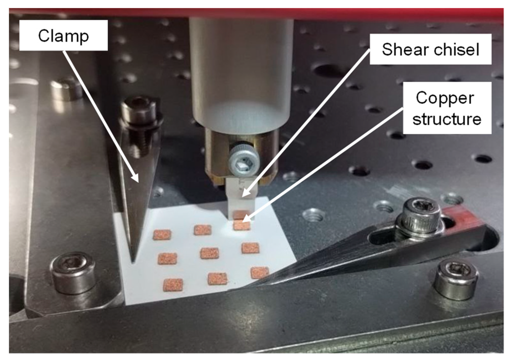
To assess the adhesion, shear testing is conducted according to DIN EN 15340 [31]. An XYZTec Condor Sigma (Panningen, The Netherlands) machine is used with a 5 mm shear chisel, a shear height of 0.05 mm, and a shear speed of 0.05 mm/s. The tested Cu structures have dimensions of 3 mm × 3 mm × 0.36 mm. Figure 3 shows the shear testing arrangement for this study.
Electrical resistance measurement is conducted by applying four-point measurements on PBF-LB/M-manufactured Cu lines, which have a length of 30 mm, a width of 1 mm, and a height of 0.36 mm. The actual geometric data is verified using a Keyence laser scanning microscope.
To evaluate the reliability of conventional electronic modules, environmental simulation tests such as the temperature shock test (TST) are applied according to the standard IEC 60068 [32]. A TST program consists of both temperature alternations and dwelling times; in this study, temperatures of −40 °C and +150 °C with dwelling times of 15 min are applied. Hereby, failures such as delamination or crack initiation can be evoked in the conductive structure, frequently owing to the different thermomechanical expansion behaviors of the material compound (CTE mismatch). Electrical resistance values and adhesion values are measured initially and after 250, 500, 750, and 1000 cycles. The geometry of the conductive lines is determined microscopically [33].
With this geometric data, the specific electrical conductivity σ is calculated using Formula (1), where R is the measured electrical resistance, l is the considered length of the sample, and A is the cross-sectional area of the conductive line.
σ = l R · A

4. Results and Discussion

The following section displays the essential results of this study, from the PBF-LB/M process to measurements of adhesion and specific electrical conductivity to the evaluation of the reliability of the copper–ceramic components.

4.1. Parameter Study of PBF-LB/M with Cu on AlN

To adapt the PBF-LB/M process to AlN substrates, four process parameters are systematically varied in a factorial design of experiments, as follows: laser power P in W, scan velocity v in mm/s, pre-heating temperature T in °C, and the height of the first layer d 1 in µm. The hatch distance h is constantly kept at 55 µm, the focus diameter of the laser d F at 48 µm, and the layer thickness d at 30 µm. With these factors, the volumetric energy density V E D is given in Formula (2):
V E D = P v · d · h
It is known from the literature that the photon density decisively influences the material behavior of the generated metal–ceramic bond [9]. Therefore, it should be noted that energy inputs of the same value do not necessarily lead to the same results if realized by different combinations of laser power and scan velocity.
The selection of the parameters and their respective values is based on preliminary investigations on Al2O3 substrates conducted at the same institute with the same machine [9].
An overview of the considered parameter settings is given in Table 2. With those parameters, 12 layers of Cu are generated; each layer has a height of 30 µm, except for the first one, whose height is varied between 30 µm and 80 µm, leading to total height values of 360 µm and 410 µm, respectively. We should note that 30 µm is a common value in PBF-LB/M [9], while the usage of 80 µm evaluates the influence of a higher first layer on adhesion and conductivity.
For adhesion assessment, Cu cubes (3 mm side length) are generated; for electrical resistance measurements, cuboids with a base area of 25 × 1 mm2 are produced (see Figure 4).

4.2. Adhesion

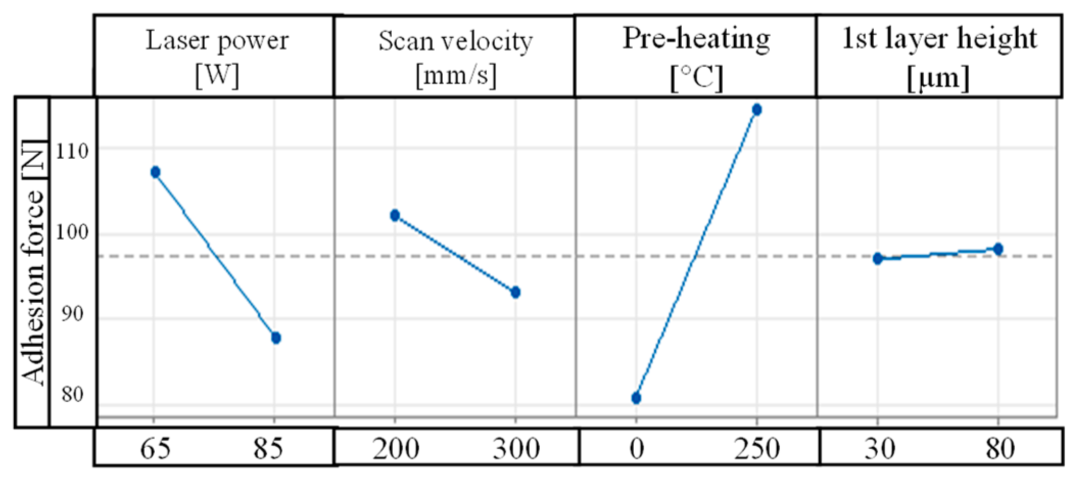
One major focus of this study lies in the evaluation of the adhesion of the processed Cu structures on the AlN substrates. For each parameter setting, six samples are produced and sheared off. The mean standard deviation is 18.8%. The evaluation of the main factors is given in Figure 5.
While the lower of the considered laser power levels leads to higher adhesion values, the scan velocity should rather be set high. More clearly, the positive effects of pre-heating on the adhesion of the Cu powder are visible. As reported in [7], pre-heating of the substrate in PBF-LB/M can successfully decrease thermal gradients during processing and influence residual stresses; also, the coupling of the laser beam into the ceramic surface is favored, leading to improved adhesion due to enhanced interlocking and material bonding at the interface. According to Figure 5, the height of the first layer is rather irrelevant to final adhesion.
A Pareto chart of standardized effects is used to identify and visualize the most important factors influencing the adhesion. It displays the absolute values of the standardized effects in descending order. The vertical, red reference line indicates the effects that are statistically significant. Accordingly, the laser power (factor A) and the pre-heating temperature (factor C) are statistically relevant to the adhesion; however, relevant interactions include scan velocity (factor B) and first layer height (factor D) (see Figure 6).
Maximum mean value of measured adhesion is 15.08 MPa (n = 6), achieved by applying a laser power of 65 W, a scanning velocity of 200 mm/s, pre-heating at 250 °C, and a first layer height of 80 µm. This adhesion value is lower than that reported in previous work achieved with PBF-LB/M-manufactured Cu on Al2O3, which reported values between 20 and 30 N/mm2 [9].
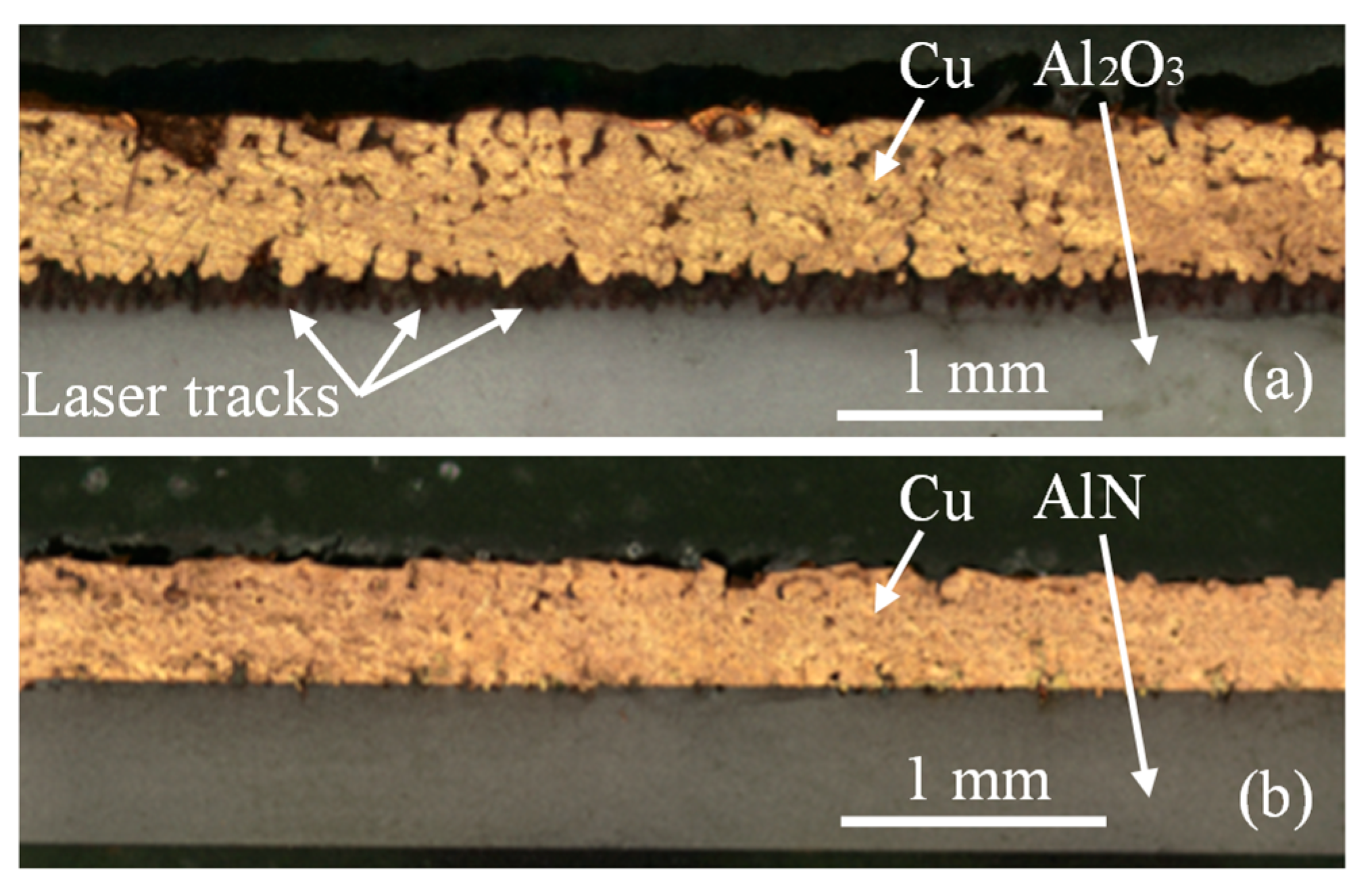
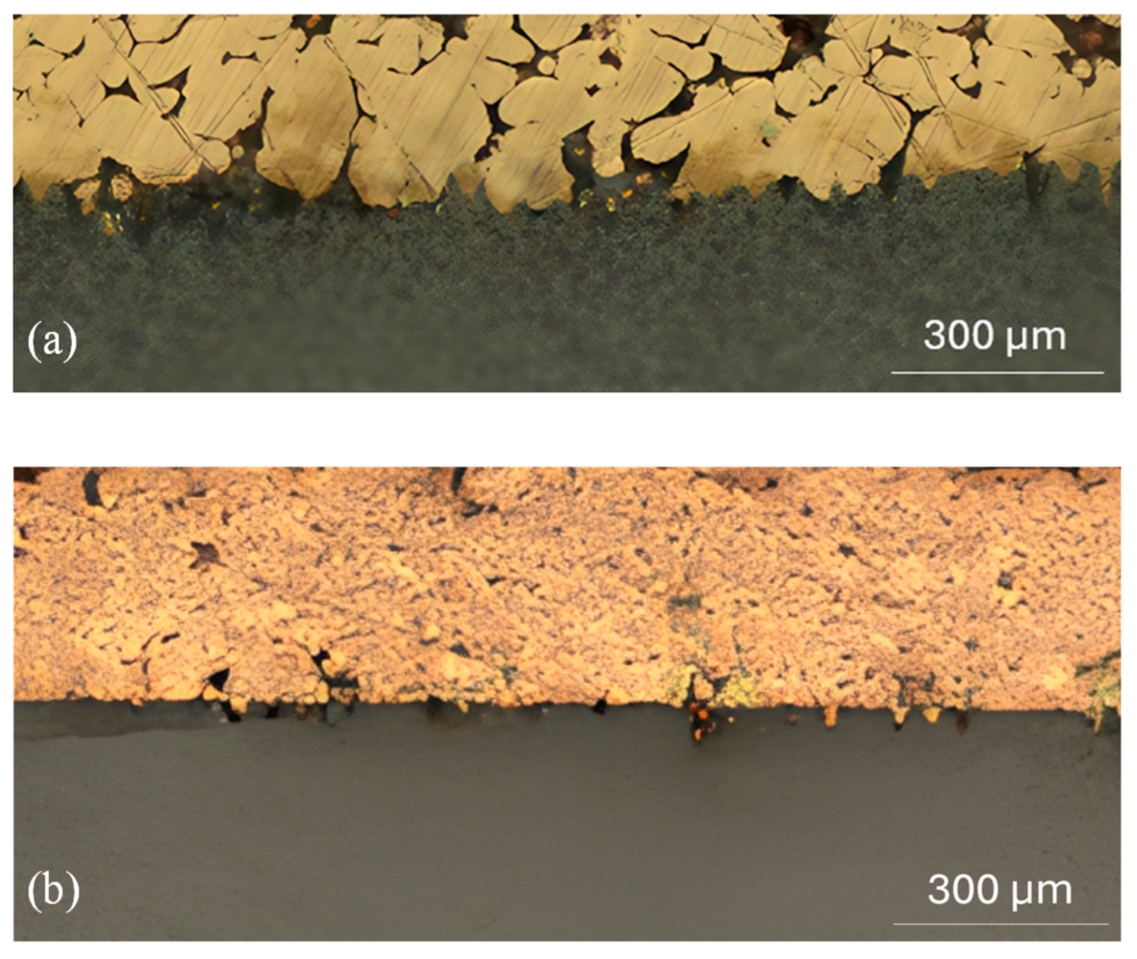
For microstructural analysis, cross-sections are prepared for PBF-LB/M-manufactured Cu on Al2O3 and AlN. As microscope pictures show, processing tracks of the laser are seen in the surface of the Al2O3 (see Figure 7a), while significantly fewer tracks are seen in the surface of AlN (see Figure 7b). The coupling of the laser beam into the AlN surface is likely inhibited by the higher hardness of AlN and by its higher thermal conductivity, which quickly dissipates parts of the heat generated by the laser beam.
The mean standard deviation of these adhesion tests turns out to be 18.8%. Thus, the process stability should be improved, and further experiments should be conducted to expand the amount of data collected.
The adhesion mechanism at work in the Cu-AlN interface is expected to be mechanical interlocking only, while Cu-Al2O3 interfaces exhibit additional chemical bonding owing to the oxygen content in the alumina surface [9,13].
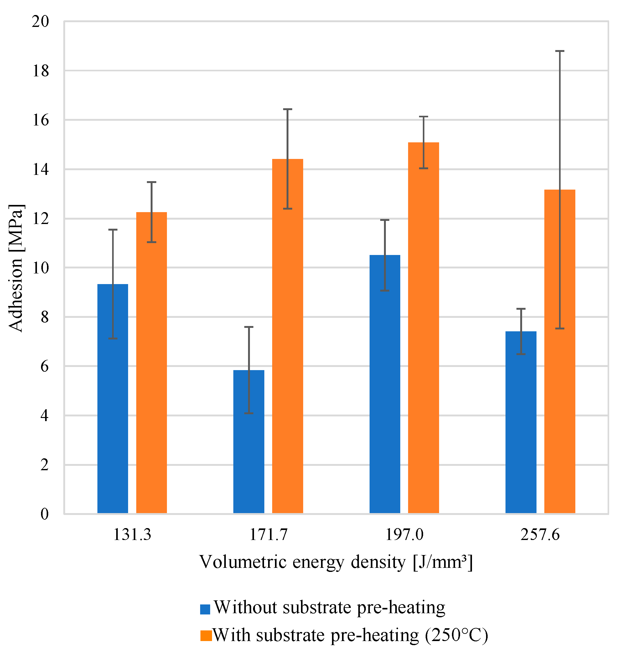
Table 3 and Figure 8 show the relationship between V E D and the resulting adhesion. V E D values between 131.3 J/mm3 and 257.6 J/mm3 are reached, while the parameter levels from Table 2 are used. The layer height is always 30 µm, except for the first one (80 µm). The adhesion values are mean values from six measurements per applied V E D .
To calculate the V E D , d = 30 µm is always used; this simplification may be justified by referring to Figure 7, where the layer height is considered the least relevant factor with regard to adhesion. With pre-heating (orange bars in Figure 9), neither a very high V E D nor a very low V E D results in the maximum adhesion. Too little energy prevents the powder from interlocking with the ceramic surface, whereas too high energy damages the surface rather than creates an interface. Also in [9], a trend is observed, which includes a rise in adhesion when V E D increases up to a maximum point, after which a decrease in adhesion occurs with further increases in V E D starting again, so the best adhesion values are reached with medium V E D values. The fracture codes showed mostly adhesion fractures with some cohesive shares.

4.3. Specific Electrical Conductivity

Since both high adhesion and high specific electrical conductivity are essential for later applications, the influence of process parameters on the electrical conductivity is also investigated. Based on the assumption that only the lower layers of the Cu structure are mainly responsible for adhesion, as suggested in [9], the Cu structure is divided into two regions, and the printing parameters for the upper layers are adjusted to increase energy density (see Figure 9).
For this part of the study, the first five layers are generated with a laser power of 65 W, a scan velocity of 300 mm/s, and a first layer height of 30 µm. The pre-heating temperature is always set to 250 °C. Three variations of process parameters for region 2 are investigated (see Table 4). An increase in the laser power to 100 W leads to σ = 18.7 MS/m (variant 1). A reduction of the scan velocity to 200 mm/s results in σ = 16.7 MS/m (variant 2), while increasing the laser power to 120 W and the scan velocity to 300 mm/s leads to σ = 18.2 MS/m (variant 3). Specimens created with this third variant are subsequently tempered in a tube furnace under a nitrogen atmosphere for 8 h at 650 °C and for 10 h at 850 °C, respectively. This enhances σ to 22.1 MS/m and 31.3 MS/m, respectively.
This data suggests that the adjustment of printing parameters is not as influential as the subsequent tempering process. Notably, maximum values of 31.3 MS/m are comparable to literature values for Al2O3 [9], which, however, considered metallization thicknesses of 600 µm, not only 360 µm, as in this study.
Cross-sections display the increasing homogeneity and growing density of the copper compound, depending on the thermal treatment. While porosity in the Cu structure is clearly visible before heat treatment (see Figure 10a), due to increased homogeneity and reduced porosity after 850 °C for 10 h (see Figure 10b), the values of the specific electrical conductivity significantly increase.

4.4. Reliability

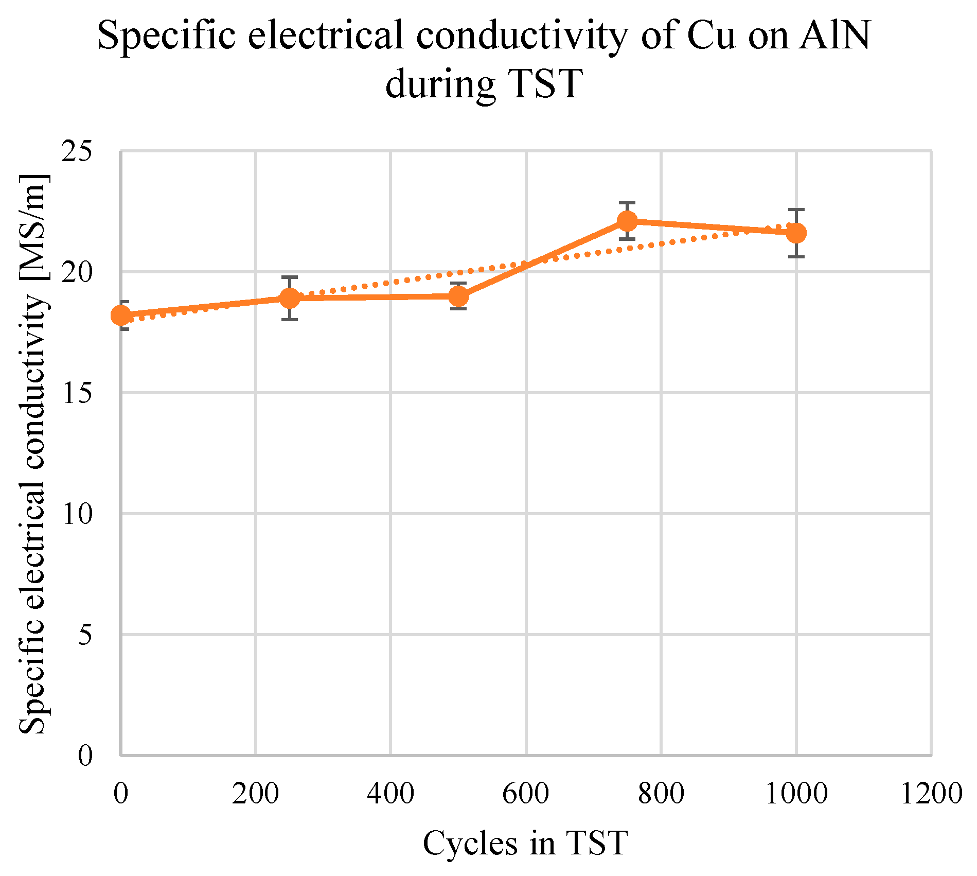
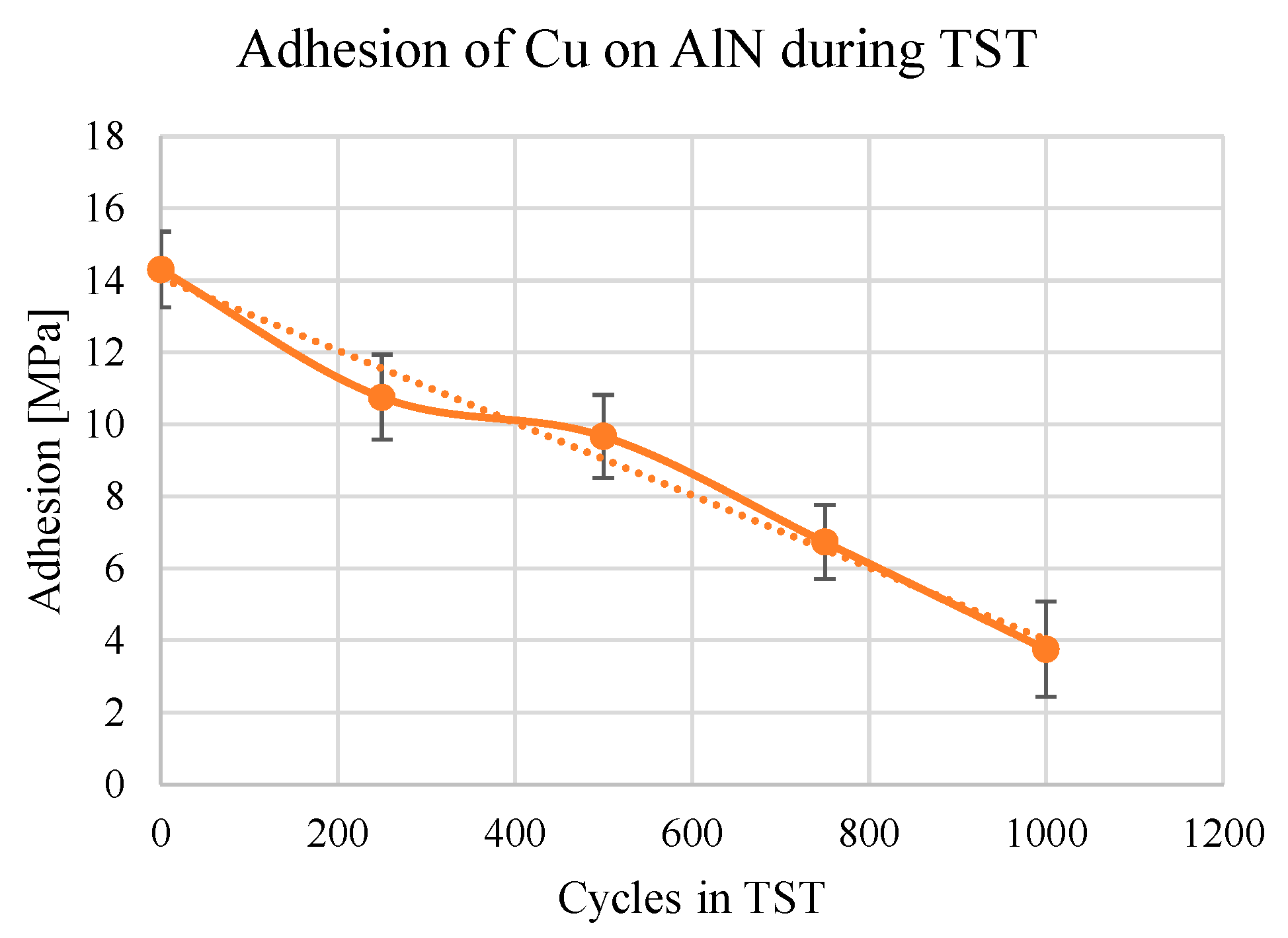
The results of reliability analysis using up to 1000 cycles in a TST are displayed in the following. Initially, the measurements of the considered samples show σ = 18.2 MS/m (n = 5) and 14.3 MPa (n = 4) in adhesion measured by shear testing (see Figure 11 and Figure 12).
The presented values are mean values of three adhesion measurements and five conductivity measurements. After 250 cycles, σ slightly increases to 18.9 MS/m, while the adhesion decreases to 10.8 MPa. In the following, σ still tends to grow, being 19 MS/m after 500 cycles and 21.6 MS/m after 1000 cycles. However, the adhesion declines to 9.7 MPa after 500 cycles and only 3.8 MPa after 1000 cycles. The results underline the relevance of aging tests for assessing the long-term reliability of additively manufactured conductive structures under the alternating thermal load. The decline in the measured adhesion values suggests ongoing thermo-mechanical damage, affecting the mechanical bonding between copper and ceramic. This is not new to copper–ceramic substrates. In [34], Cu-AlN substrates with a metallization thickness of 300 µm, manufactured with conventional DCB technology, are tested under thermal loads between −30 °C and +180 °C with a dwelling time of 30 min. This is neither exactly the geometry nor the testing condition used in this study, but fairly comparable, nonetheless. The results show that all samples fail after 50 cycles [34]. In [35], Cu-AlN substrates with a thickness of 300 µm, manufactured with conventional AMB technology, are tested under thermal loads between −55 °C and +150 °C with a dwell time of 15 min. After 40 cycles, more than 50% of the samples already display some degree of delamination. After 80 cycles, adhesion measured by the peeling test is reduced by up to 50%. Compared to these references, a 25% decrease in adhesion after 250 cycles in this study seems to be quite acceptable.
In [9], no failure is reported in PBF-LB/M-manufactured copper structures on Al2O3 with a metallization thickness of 600 µm after 240 cycles in TST (−30 °C/+150 °C, dwell time: 30 min). With thermal post-treatment of the samples, up to 615 cycles without reported failure are achievable. The higher values achieved by PBF-LB/M samples compared to conventional substrates may result from the lower porosity of the metallization layer, which in turn reduces the CTE mismatch [9].
The noted rise in specific electrical conductivity in this study can be explained by post-sintering effects, that is, the ongoing exposure of the samples to 150 °C may trigger further physical contact between copper powder particles, forming sintering necks between particles, as known from conductive inks in the field of printed electronics [33]. Then, the increased contact area of copper particles slightly increases the electrical conductivity values.

5. Summary and Outlook

This work investigated the use of AlN substrates in a laser-based powder bed fusion process of Cu powder for ceramic circuit carriers in power electronic applications.
While hatch distance and focus diameter of the laser were kept constant during the PBF-LB/M process, laser power, scan velocity, pre-heating temperature, and the height of the first layer were systematically varied and evaluated. Particularly influential on positive results in adhesion of Cu onto AlN was the usage of substrate pre-heating as well as setting the laser power not too high (65 W instead of 85 W). For the specific electrical conductivity σ , a thermal post-treatment step proved promising. Determined conductivity values reached σ = 31 MS/m, which is comparable to literature values for Al2O3. Adhesion reached 15 MPa, which is lower than comparable investigations with Al2O3, probably owing to the lack of chemical bonding between Cu and AlN. Notably, TST analysis outlined a relatively long stability of the additively manufactured Cu-AlN specimens compared to conventional DCB.
To conclude, the feasibility of the PBF-LB/M process of Cu powder on AlN substrates was demonstrated. In order to increase adhesion, further studies should evaluate the influence of pre-oxidizing AlN substrates in a furnace on the adhesion of Cu structures, creating an oxide layer on the AlN surface (see [36,37,38]), which is expected to enable not only mechanical interlocking but also chemical bonding between the copper and the ceramic. Direct experimental validation, such as TEM/EDS analysis of the Cu/AlN interface, should be used to confirm elemental diffusion/reaction layers. Furthermore, future research should include adhesion properties of the tempered samples from Table 4, since the influence of the thermal post-treatment on the adhesion of Cu on AlN has not yet been investigated.
Moreover, the connection of components like bare dies using soldering processes onto the additively manufactured Cu structures has to be investigated in future work in order to specifically exploit the high potential of additive manufacturing processes for real power electronic applications.

Author Contributions

Conceptualization, D.U.; Methodology, D.U.; Validation, C.H.; Investigation, T.T. and D.U.; Writing—original draft, D.U.; Writing—review & editing, C.H.; Visualization, M.O.; Supervision, J.F. and F.R.; Project administration, N.T.; Funding acquisition, D.U. All authors have read and agreed to the published version of the manuscript.

Funding

This research was funded by the German Aerospace Center (DLR) within the Research Association Mechatronic Integrated Devices 3-D MID e.V. in the IGF-project 01IF22835N, “MultiPower”.

Data Availability Statement

The data presented in this study are available on request from the corresponding author.

Conflicts of Interest

The authors declare no conflicts of interest.

References

  1. Lopera, L.; Rodriguez, R.; Yakout, M.; Elbestawi, M.; Emadi, A. Current And Potential Applications Of Additive Manufacturing For Power Electronics. IEEE Open J. Power Electron. 2021, 2, 33–42. [Google Scholar] [CrossRef]
  2. Yang, Y.; Dorn-Gomba, L.; Rodriguez, R.; Mak, C.; Emadi, A. Automotive Power Module Packaging: Current Status and Future Trends. IEEE Access 2020, 8, 160126–160144. [Google Scholar] [CrossRef]
  3. Khazaka, R.; Mendizabal, L.; Henry, D.; Hanna, R. Survey of High-Temperature Reliability of Power Electronics Packaging Components. IEEE Trans. Power Electron. 2015, 30, 2456–2464. [Google Scholar] [CrossRef]
  4. CeramTec. Advanced Ceramics for Electronic Applications. Material Properties of Rubalit, Alunit, Zirkolit and Sinalit. 2024. Available online: https://www.ceramtec-industrial.com/fileadmin/user_upload/Corporate/11_Downloads/06_Electronic_Heatsinks/Datasheet_Electronic_Applications.pdf (accessed on 30 May 2025).
  5. Kumar, A.; Moradour, M.; Losito, M.; Franke, W.-T.; Ramasamy, S.; Baccoli, R.; Gatto, G. Wide Band Gap Devices and Their Application in Power Electronics. Energies 2022, 15, 9172. [Google Scholar] [CrossRef]
  6. Rafin, S.; Ahmed, R.; Mohammed, O. Wide Band Gap Semiconductor Devices for Power Electronic Converters. In Proceedings of the 2023 Fourth International Symposium on 3D Power Electronics Integration and Manufacturing (3D-PEIM), Miami, FL, USA, 1–3 February 2023; pp. 1–8. [Google Scholar] [CrossRef]
  7. Hecht, C.; Ockel, M.; Stoll, T.; Franke, J. Fabrication of metal-ceramic substrates by laser powder bed fusion using a high-power green laser and high temperature preheating. In Proceedings of the Laser 3D Manufacturing XI27, San Francisco, CA, USA, 27 January–1 February 2024; ISBN 9781510670129. [Google Scholar]
  8. Syed-Khaja, A.; Schwarz, D.; Franke, J. Advanced substrate and packaging concepts for compact system integration with additive manufacturing technologies for high temperature applications. In Proceedings of the 2015 IEEE CPMT Symposium Japan (ICSJ), Kyoto, Japan, 9–11 November 2015; pp. 156–159, ISBN 978-1-4799-8814-3. [Google Scholar]
  9. Stoll, T. Laser Powder Bed Fusion von Kupfer auf Aluminiumoxid-Keramiken; FAU University Press: Erlangen, Germany, 2023; ISBN 978-3-96147-632-9. [Google Scholar]
  10. Rogers Corp.; CURAMIK (R). curamik (R) Ceramic Substrates. Technical Datasheet. 2019. Available online: https://rogerscorp.com/-/media/project/rogerscorp/documents/advanced-electronics-solutions/english/product-information/curamik-ceramic-substrates-product-information-and-data-sheet.pdf (accessed on 26 May 2025).
  11. Specovius, J. Grundkurs Leistungselektronik. Bauelemente, Schaltungen, Systeme. 7; Springer: Wiesbaden, Germany, 2015; ISBN 978-3658033088. [Google Scholar]
  12. Eustathopoulos, N.; Hodaj, F.; Kozlova, O. The wetting process in brazing. In Advances in Brazing; Elsevier: Amsterdam, The Netherlands, 2013; pp. 3–30. ISBN 9780857094230. [Google Scholar]
  13. Hromadka, K.; Stulik, J.; Reboun, J.; Hamacek, A. DBC Technology for Low Cost Power Electronic Substrate Manufacturing. Procedia Eng. 2014, 69, 1180–1183. [Google Scholar] [CrossRef]
  14. Chua, S.; Siow, K.S. Microstructural studies and bonding strength of pressureless sintered nano-silver joints on silver, direct bond copper (DBC) and copper substrates aged at 300 °C. J. Alloys Compd. 2016, 687, 486–498. [Google Scholar] [CrossRef]
  15. Schmenger, M.; Meisser, M.; Hamilton, D.; Leyrer, B.; Bernd, M.; Mawby, P. Highly integrated power modules based on copper thick-film-on-DCB for high frequency operation of SiC semiconductors—Design and manufacture. In Proceedings of the 2015, 17th European Conference on Power Electronics and Applications (EPE’15 ECCE-Europe), Geneva, Switzerland, 8–10 September 2015; pp. 1–8. [Google Scholar] [CrossRef]
  16. Durand, C.; Klingler, M.; Coutellier, D.; Naceur, H. Power Cycling Reliability of Power Module: A Survey. IEEE Trans. Device Mater. Reliab. 2016, 16, 80–97. [Google Scholar] [CrossRef]
  17. DIN EN ISO/ASTM 52900; Additive Fertigung. DIN Deutsches Institut fuer Normung e.V. Beuth Verlag GmbH: Berlin, Germany, 2022.
  18. Colopi, M.; Caprio, L.; Demir, A.G.; Previtali, B. Selective laser melting of pure Cu with a 1 kW single mode fiber laser. Procedia CIRP 2018, 74, 59–63. [Google Scholar] [CrossRef]
  19. Ikeshoji, T.-T.; Nakamura, K.; Yonehara, M.; Imai, K.; Kyogoku, H. Selective Laser Melting of Pure Copper. JOM 2018, 70, 396–400. [Google Scholar] [CrossRef]
  20. Jadhav, S.D.; Dadbakhsh, S.; Goossens, L.; Kruth, J.-P.; Humbeeck, J.V.; Vanmeensel, K. Influence of selective laser melting process parameters on texture evolution in pure copper. J. Mater. Process. Technol. 2019, 270, 47–58. [Google Scholar] [CrossRef]
  21. Kaden, L.; Matthäus, G.; Ramm, R.; Ullsperger, T.; Seyfarth, B.; Nolte, S. Additive manufacturing of pure copper using ultrashort laser pulses. In Proceedings of the Laser 3D Manufacturing VI, San Francisco, CA, USA, 2–7 February 2019; ISBN 9781510624603. [Google Scholar]
  22. Shibata, T.; Tsukamoto, M.; Sato, Y.; Masuno, S. Effect of input energy on densification for pure copper fabricated by SLM with blue diode laser. In Proceedings of the Laser 3D Manufacturing VI, San Francisco, CA, USA, 2–7 February 2019; ISBN 9781510624603. [Google Scholar]
  23. Stoll, T.; Kirstein, M.; Franke, J. A novel approach of copper-ceramic-joints manufactured by selective laser melting. In Proceedings of the Material Technologies and Applications to Optics, Structures, Components, and Sub-Systems IV, San Francisco, CA, USA, 11–15 August 2019; ISBN 9781510628953. [Google Scholar]
  24. Hecht, C.; Schueller, D.; Utsch, D.; Stoll, T.; Franke, J. Investigations on processing copper-titanium powder blends via PBF-LB/M. In Proceedings of the Lasers in Manufacturing Conference, Munich, Germany, 26–29 June 2023. [Google Scholar]
  25. Hecht, C.; Schadow, E.; Sprenger, M.; Häußler, F.; Stoll, T.; Franke, J. Additive Metallization of Alumina with Copper-Titanium Powder Blends for Power Electronic Applications. In Proceedings of the 2023 24th European Microelectronics and Packaging Conference & Exhibition (EMPC), Cambridge, UK, 11–14 September 2023; pp. 1–6, ISBN 978-0-9568086-9-1. [Google Scholar]
  26. Hecht, C.; Sprenger, M.; Franke, J. Laser powder bed fusion of titanium alloyed copper powder for power electronic substrates. In Proceedings of the 2024 47th International Spring Seminar on Electronics Technology (ISSE), Prague, Czech Republic, 15–19 May 2024; pp. 1–6, ISBN 979-8-3503-8547-2. [Google Scholar]
  27. Wallis, C.; Buchmayr, B.; Bermejo, R.; Supancic, P. Fabrication of 3D metal-ceramic (Al-AlN) architectures using laser-powder bed fusion process. Addit. Manuf. 2021, 38, 101799. [Google Scholar] [CrossRef]
  28. Werdecker, W.; Aldinger, F. Aluminum Nitride-An Alternative Ceramic Substrate for High Power Applications in Microcircuits. IEEE Trans. Compon. Hybrids Manuf. Technol. 1984, 7, 399–404. [Google Scholar] [CrossRef]
  29. Harris, J.H. Sintered aluminum nitride ceramics for high-power electronic applications. JOM 1998, 50, 56–60. [Google Scholar] [CrossRef]
  30. Hickman, A.L.; Chaudhuri, R.; Bader, S.J.; Nomoto, K.; Li, L.; Hwang, J.C.M.; Xing, H.G.; Jena, D. Next generation electronics on the ultrawide-bandgap aluminum nitride platform. Semicond. Sci. Technol. 2021, 36, 044001. [Google Scholar] [CrossRef]
  31. DIN EN 15340; Thermisches Spritzen—Bestimmung des Scherbeanspruchungs widerstandes bei thermisch gespritzten Schichten. DIN Deutsches Institut fuer Normung e.V. Beuth Verlag GmbH: Berlin, Germany, 2007.
  32. IEC 60068-2-14; Umweltpruefungen. DIN Deutsches Institut fuer Normung e.V. Beuth Verlag GmbH: Berlin, Germany, 2000.
  33. Utsch, D.; Häußler, F.; Sprenger, M.; Zirn, J.; Franke, J. Reliability of Piezojet-Printed Conductive Lines on Alumina Substrates Produced by Fused Filament Fabrication. In Proceedings of the 2023 15th International Congress Mechatronic Integration Discourse (MID), Amberg, Germany, 21–22 June 2023; pp. 1–6, ISBN 979-8-3503-7473-5. [Google Scholar]
  34. Dupont, L.; Lefebvre, S.K.; Bontemps, S. Evaluation of Substrate Technologies under High Temperature Cycling. In Proceedings of the International Conference on Integrated Power Systems, Naples, Italy, 7–9 June 2006. [Google Scholar]
  35. Mitic, G.; Beinert, R.; Klofac, P.; Schultz, H.J.; Lefranc, G. Reliability of AlN substrates and their solder joints in IGBT power modules. Microelectron. Reliab. 1999, 39, 1159–1164. [Google Scholar] [CrossRef]
  36. Lee, J.W.; Radu, I.; Alexe, M. Oxidation behavior of AlN substrate at low temperature. J. Mater. Sci. Mater. Electron. 2002, 13, 131–137. [Google Scholar] [CrossRef]
  37. Wei, X.; Xu, H.; Zhan, J.; Zhang, H.; Cao, Y.; Cui, S.; Tang, W. Comparative studies on microstructures, strengths and reliabilities of two types of AlN direct bonding copper substrates. Ceram. Int. 2018, 44, 18935–18941. [Google Scholar] [CrossRef]
  38. Yeh, C.-T.; Tuan, W.-H. Oxidation mechanism of aluminum nitride revisited. J. Adv. Ceram. 2017, 6, 27–32. [Google Scholar] [CrossRef]
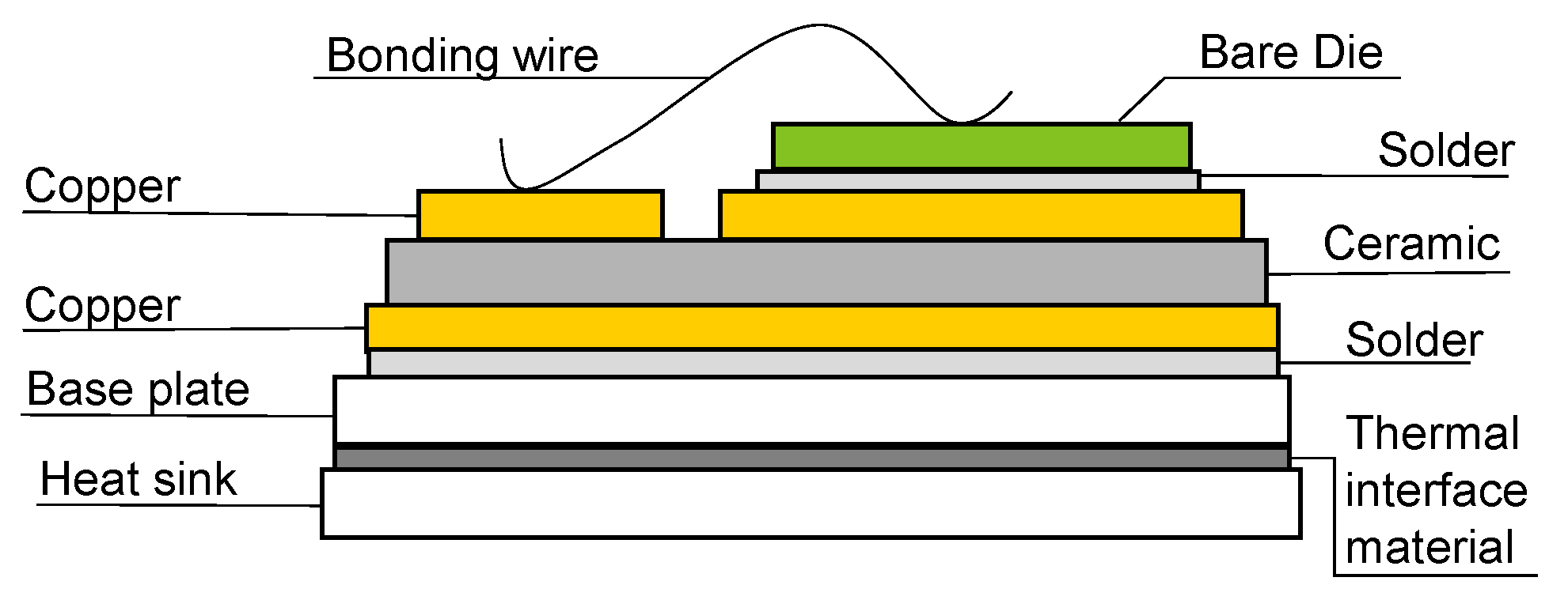
Figure 1. Typical build-up of a conventional power module based on [11].
Ceramics 08 00105 g001
Figure 2. Schematic representation of the PBF-LB/M process based on [8].
Ceramics 08 00105 g002
Figure 3. Shear testing of PBF-LB/M-manufactured copper on a ceramic substrate with an XYZTec Condor Sigma.
Ceramics 08 00105 g003
Figure 4. AlN substrate with PBF-LB/M-manufactured Cu.
Ceramics 08 00105 g004
Figure 5. Main factor diagram for mean adhesion values of PBF-LB/M-manufactured Cu on AlN.
Ceramics 08 00105 g005
Figure 6. Pareto diagram of standardized effects for adhesion on AlN (α = 0.05).
Ceramics 08 00105 g006
Figure 7. Cross-sections of PBF-LB/M-manufactured Cu on Al2O3 (a) and AlN (b) substrates.
Ceramics 08 00105 g007
Figure 8. Relationship between volumetric energy density during PBF-LB/M process and adhesion of Cu on AlN.
Ceramics 08 00105 g008
Figure 9. Two-region buildup of Cu structure.
Ceramics 08 00105 g009
Figure 10. Cross-sections of Cu on AlN before (a) and after (b) tempering in nitrogen atmosphere for 10 h at 850 °C.
Ceramics 08 00105 g010
Figure 11. Development of specific electrical conductivity values of PBF-LB/M-manufactured copper on AlN during TST (−40 °C/+150 °C; dwell time: 15 min).
Ceramics 08 00105 g011
Figure 12. Development of adhesion values (shear testing) of PBF-LB/M manufactured Cu on AlN during TST (−40 °C/+150 °C; dwell time: 15 min).
Ceramics 08 00105 g012
Table 2. Used parameter settings in the PBF-LB/M process.
FactorLaser Power
[W]
Scan Velocity [mm/s]Pre-Heating Temperature [°C]First Layer Height
[µm]
Level 165200030
Level 28530025080
Table 3. Achieved volumetric energy density (VED) as a function of laser power and scan velocity.
FactorsLaser Power [W]Scan Velocity [mm/s]VED
[J/mm3]
Variant 165300131.3
Variant 285300171.7
Variant 365200197.0
Variant 485200257.6
Table 4. Specific electrical conductivity σ as a function of varying parameters and subsequent tempering.
ParametersLaser Power [W]Scan Velocity [mm/s] Specific   Electrical   Conductivity   σ [MS/m]
Layers 1–565300-
Layers 6–12 (var. 1)10030018.7
Layers 6–12 (var. 2)10020016.7
Layers 6–12 (var. 3)12030018.2
Var. 3 and tempering with 650 °C/8 h22.1
Var. 3 and tempering with 850 °C/10 h31.3
Disclaimer/Publisher’s Note: The statements, opinions and data contained in all publications are solely those of the individual author(s) and contributor(s) and not of MDPI and/or the editor(s). MDPI and/or the editor(s) disclaim responsibility for any injury to people or property resulting from any ideas, methods, instructions or products referred to in the content.