Article

Structural and Dielectric Properties of Titania Co-Doped with Yttrium and Niobium: Experimental Evidence and DFT Study

by
Deborah Y. B. Silva
,
Reginaldo Muccillo
and
Eliana N. S. Muccillo
*
Energy and Nuclear Research Institute–IPEN, São Paulo 05508-000, SP, Brazil
*
Author to whom correspondence should be addressed.
Ceramics 2024, 7(1), 411-425; https://doi.org/10.3390/ceramics7010026
Submission received: 23 January 2024 / Revised: 7 March 2024 / Accepted: 15 March 2024 / Published: 17 March 2024
(This article belongs to the Special Issue Advances in Ceramics, 2nd Edition)

Abstract

:
This work explores the impact of the sintering temperature and co-dopant contents on the microstructure and dielectric properties of (Y0.5Nb0.5)xTi1−xO2 (0.025 ≤ x ≤ 0.10) ceramics synthesized by the solid state reaction method. The physical mechanism underlying the colossal electric permittivity was systematically investigated with experimental methods and first principles calculations. All specimens exhibited the characteristic tetragonal structure of rutile, besides secondary phases. A niobium- and yttrium-rich secondary phase emerged at the grain boundaries after heating at 1500 °C, changing the main sintering mechanism. The highest value of the electric permittivity (13499 @ 60 °C and 10 kHz) was obtained for (Y0.5Nb0.5)0.05Ti0.95O2 sintered at 1480 °C, and the lowest dissipation factor (0.21@ 60 °C and 10 kHz) for (Y0.5Nb0.5)0.1Ti0.90O2 sintered at 1500 °C. The dielectric properties of Y3+ and Nb5+ co-doped TiO2 are attributed to the internal barrier layer capacitance (IBLC) and electron-pinned dipole defect (EPDD) mechanisms.

1. Introduction

Ceramic materials are relevant in the electronic industry, due to their characteristics like durability and stability when exposed to severe conditions. Dielectric ceramics with colossal electric permittivity (ε′), in general higher than 1000, have been intensively investigated over the last decades, due to their potential application in several technological devices such as sensors and filters, and for high-energy storage [1,2,3]. Examples of dielectric ceramics with colossal electric permittivity are pure and doped BaTiO3 (BTO), CaCu3Ti4O12 (CCTO), and co-doped NiO [4,5,6]. Application of dielectric ceramics in microelectronics requires a low dissipation factor (tan δ) and good stability over wide ranges of temperature and frequency.
Titanium oxide, typically found with the rutile structure, displays a wide range of technological applications, due to its interesting electrical and photocatalytic properties, among others. Those special properties are attributed to deviation from stoichiometry and the presence of point defects within the TiO2 lattice [7]. Pure TiO2 exhibits a moderate electric permittivity (ε′~200 at room temperature [8]). In the last decade, TiO2 co-doped with acceptor and donor cations has emerged as a new family of dielectric ceramics with promising properties such as colossal permittivity and low dissipation factor [9,10,11,12,13]. The combination of the pure titanium oxide properties with those acquired by co-doping opens a promising route to obtain high-performance dielectric ceramics for applications in microelectronics and energy storage devices.
The mechanism underlying the impressive properties of co-doped TiO2 is still unclear. A model based on electron-pinned defect dipoles (EPDD) was first proposed to explain the colossal permittivity of TiO2 co-doped with niobium and indium oxide. The model was based on defect analysis substantiated by experimental results (X-ray diffraction, X-ray photoelectron spectroscopy and electron paramagnetic resonance) coupled with density functional theory (DFT) modeling [9]. The introduction of donor cations such as Nb5+ in the rutile lattice promoted reduction of some Ti4+ ions to Ti3+ and yielded free electrons. In addition, incorporation of acceptor cations like In3+ assisted in localizing those defects and led to the creation of oxygen vacancies. These effects are described by the following defect reactions:
2 T i O 2 + M 2 O 5 2 T i T i + 2 M T i + 8 O O + 1 2 O 2
T i 4 + + e T i 3 +
N 2 O 3 2 N T i + V O . . + 3 O o
where M and N stand for the donor and acceptor cations, respectively.
The DFT modeling revealed the changes in the supercells of TiO2 containing donor and acceptor cations leading to distinct defect structures, namely the triangular I n 2 3 + V O · · T i 3 + and the diamond N b 2 5 + T i 3 + A T i (A = Ti4+, Ti3+, In3+) complexes. Those complexes were obtained for the low energy configuration. Structures lacking either the triangular or the diamond complexes were found to be energetically less favorable, emphasizing the significance of both defect structures for stability. These complexes were found to be correlated according to configuration energy minimization leading to large clusters with localized electrons, thereby reducing the dissipation factor [9]. According to this model, these clusters of defects act inside the grains and not at grain boundaries or other interfaces.
Other models are the well-known internal barrier layer capacitance (IBLC) and the surface barrier layer capacitance (SBLC) related to interfaces; the former occurs at the grain boundaries, due to a Schottky type potential barrier formed in materials consisting of conducting grains and insulating grain boundaries; the latter is due to the interface between the dielectric material and the electrodes.
Several factors may influence the dielectric properties of co-doped TiO2 ceramics, such as the difference in the ionic radii of the co-dopants and that of the host (Ti), secondary phases, compositional gradients, and other microstructure features [10,14,15,16]. The microstructure of ceramics may be tailored by the processing steps, particularly by the sintering process. In vanadium and tantalum co-doped TiO2, for example, increases in both the electric permittivity and thermal stability of the ceramic with increasing grain size were reported [17].
The dielectric properties of yttrium and niobium co-doped TiO2 prepared by the combustion method [18] and by the solid-state reaction method [19] were reported to exhibit colossal permittivity, attributed to the IBLC model. In this work, a systematic study on the influence of the sintering temperature and total co-dopant contents on the microstructure, electrical and dielectric properties of (Y0.5Nb0.5)xTi1−xO2 (hereafter YNTO) ceramics prepared by the solid state reaction method is reported. The main purposes were to evaluate the effects of the sintering temperature and concentration of co-dopants on the final microstructure, and on the microstructure-dependent electrical and dielectric properties of TiO2. In addition, theoretical calculations based on DFT were undertaken to correlate the dielectric properties and the local structure and induced defects in co-doped TiO2.

2. Materials and Methods

2.1. Preparation of Materials

Polycrystalline ceramics of Y and Nb co-doped TiO2 with nominal composition (Y0.5Nb0.5)xTi1−xO2, x = 0.025, 0.05 and 0.10 were prepared by the solid-state reaction method. The starting materials were titanium oxide, TiO2 (99.5%, Alfa Aesar, Ward Hill, MA, USA), yttrium oxide, Y2O3 (99.99%, Sigma Aldrich, St. Louis, MO, USA) and niobium oxide, Nb2O5 (99.95%, Alfa Aesar, Ward Hill, MA, USA).
The TiO2 and Nb2O5 powders were dried in an oven at 100 °C overnight to remove the physically adsorbed water. The Y2O3 precursor was thermally treated at 800 °C for 2 h to eliminate residual carbonates and ammonia. Afterwards, stoichiometric amounts of the oxides were wet ball milled for 5 h with isopropyl alcohol and yttria stabilized zirconia as milling media to promote an intimate mixture and random distribution of the powder particles. After drying, the milled powder mixture was calcined at 1100 °C for 1 h, and then dry ball milled for 5 h for deagglomeration. Polyvinyl alcohol (PVA, QEEL, São Paulo, Brazil, molecular weight = 100,000) organic binder was added (3 wt.%) to the powder mixture and homogenized under ultrasound to improve the mechanical strength of the conformed samples. Disc-shaped pellets were prepared by uniaxial pressing (Kratos, Z2T, São Paulo, Brazil) in a stainless steel die (ϕ 10 mm and 2 mm thickness), followed by cold isostatic pressing (National Forge Co., Irvine, PA, USA) at 200 MPa. Sintering experiments were conducted in a resistive furnace (Lindberg, Blue M, Watertown, NY, USA) with dwell temperatures of 1480 and 1500 °C and soaking time of 4 h. Sintered specimens are hereafter named YNTO2.5, YNTO5 and YNTO10 for x = 0.025, 0.05 and 0.10, respectively.

2.2. Characterization

The structural characterization of powders and sintered pellets was performed by X-ray diffraction (Bruker–AXS, D8 Advance, Karlsruhe, Germany) with Cu Kα radiation (λ = 1.54056 Å), in the 20° ≤ 2θ ≤ 80° range, with 0.05° step size and 2 s counting time per step. Peak identification was carried out with PDF files: 73-1765 (TiO2), 27-1313 (Nb2O5) and 82-2415 (Y2O3). The sintered pellets were polished, thermally etched at 1380 ºC for 30 min, and coated with carbon film for microstructure characterization. The main microstructure features were observed in a field emission gun scanning electron microscope, SEM (FEI, Inspect F50, Brno, Czech Republic) with secondary electrons. The mean grain size was estimated with the ImageJ (1.4.3.67 version) software. Energy dispersive spectroscopy, EDS (Octane Elect Plus, Pleasanton, CA, USA) coupled to the SEM was utilized for elemental mapping.
Electrical characterization of sintered pellets was carried out by electrochemical impedance spectroscopy, EIS (Solartron, SI 1260, Allentown, PA, USA) in the 10 to 106 Hz range, with 200 mV of applied signal. For electrical measurements, silver paste was applied onto pellet surfaces and cured at 400 °C.

2.3. Computational Details
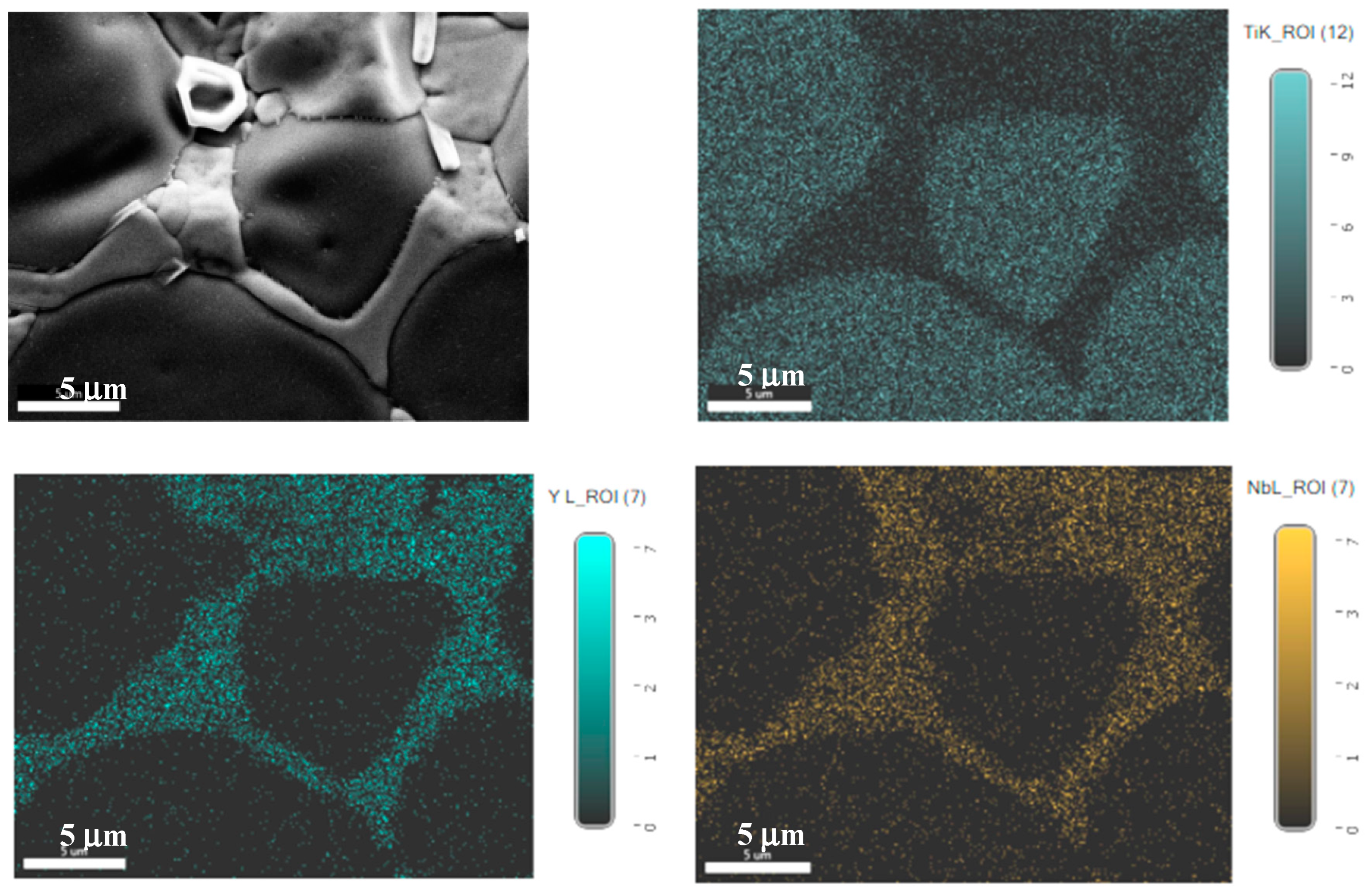
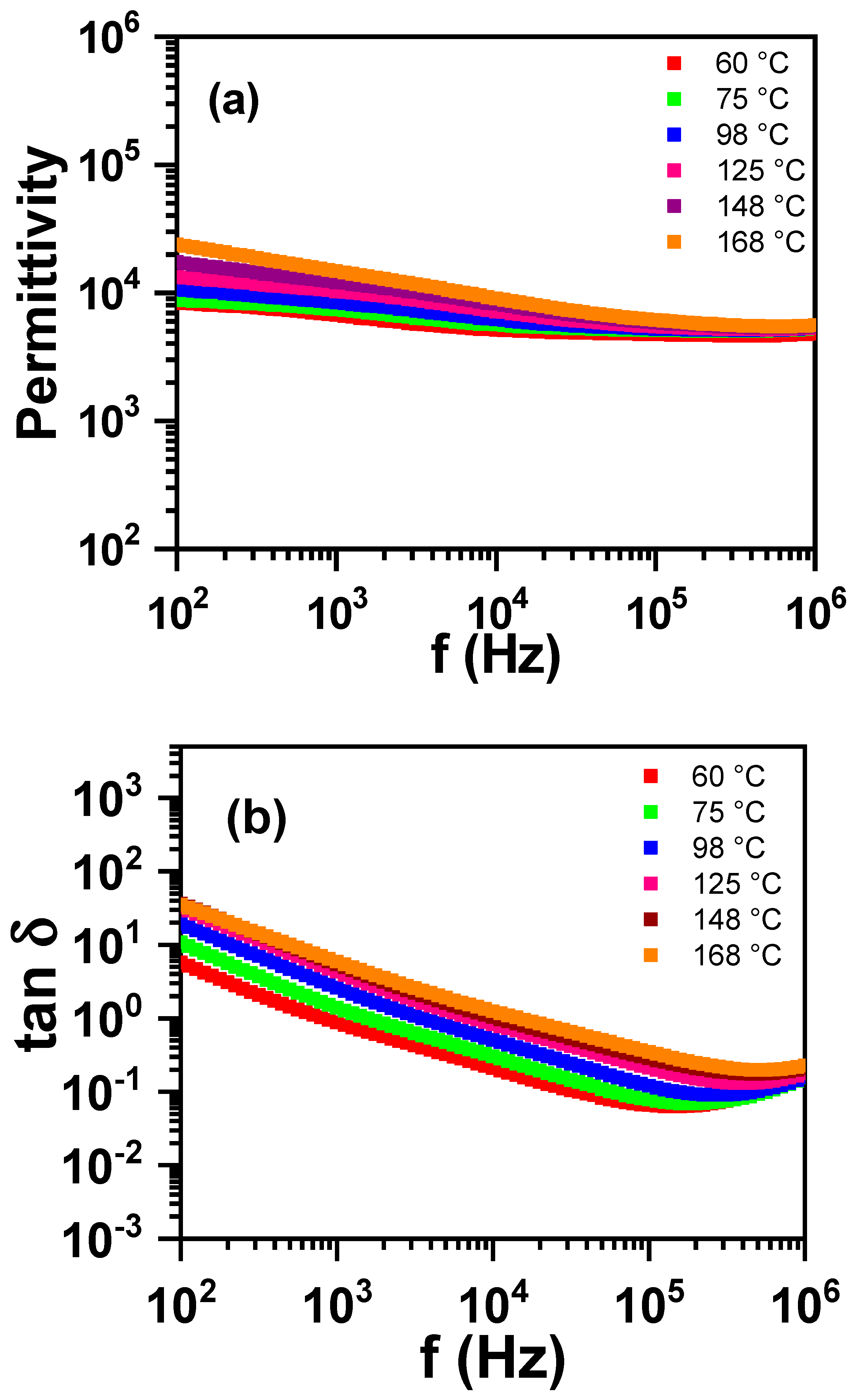
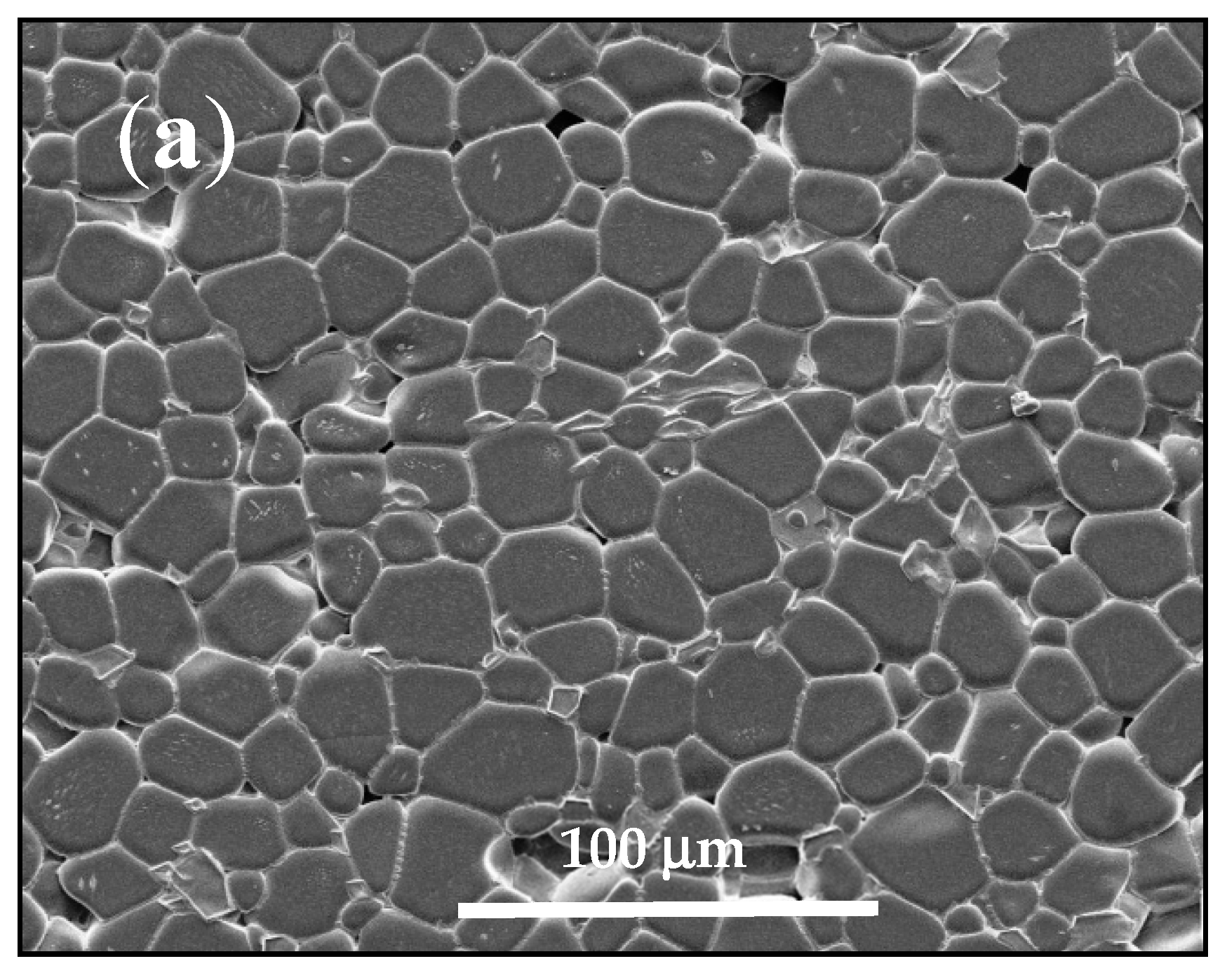
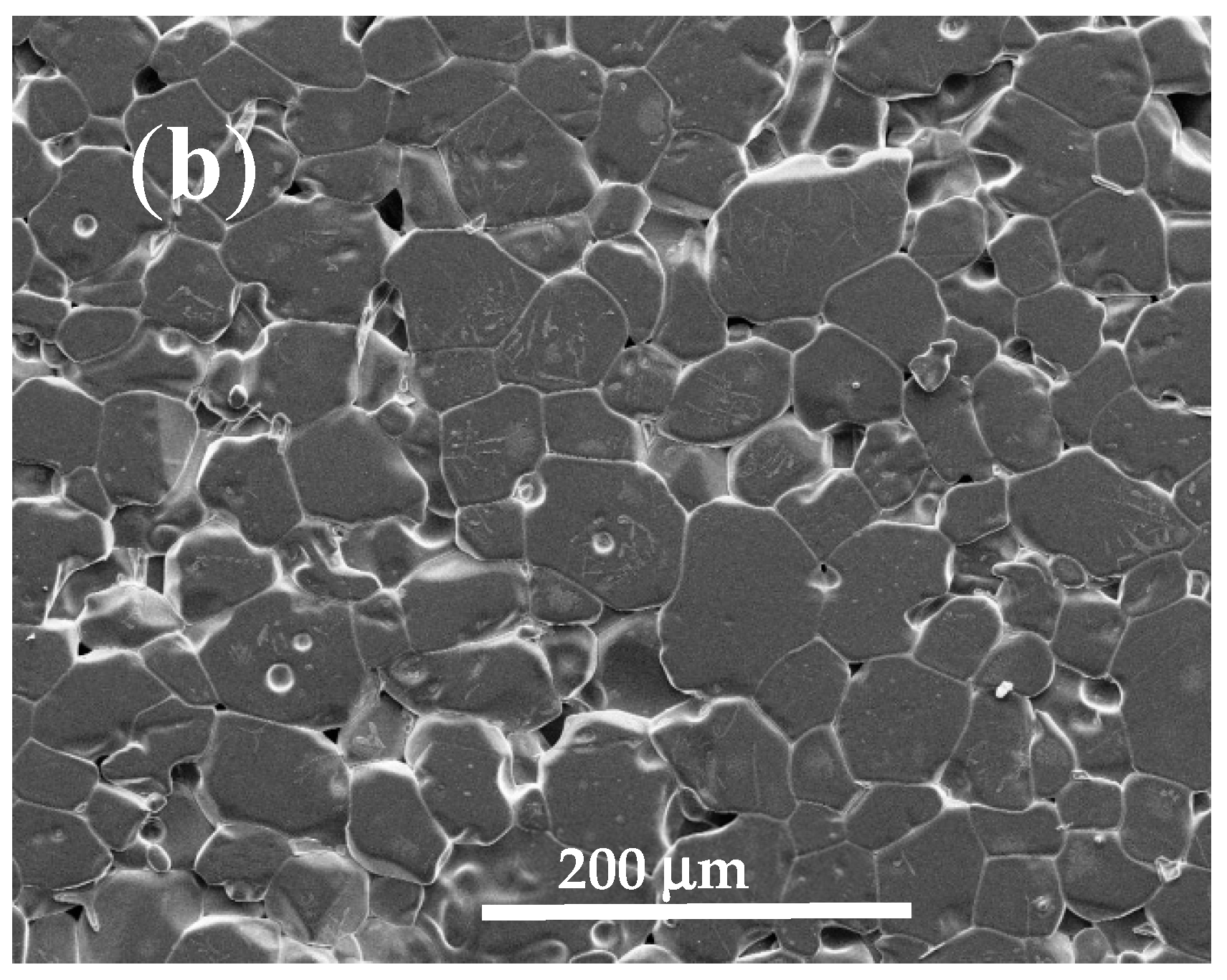
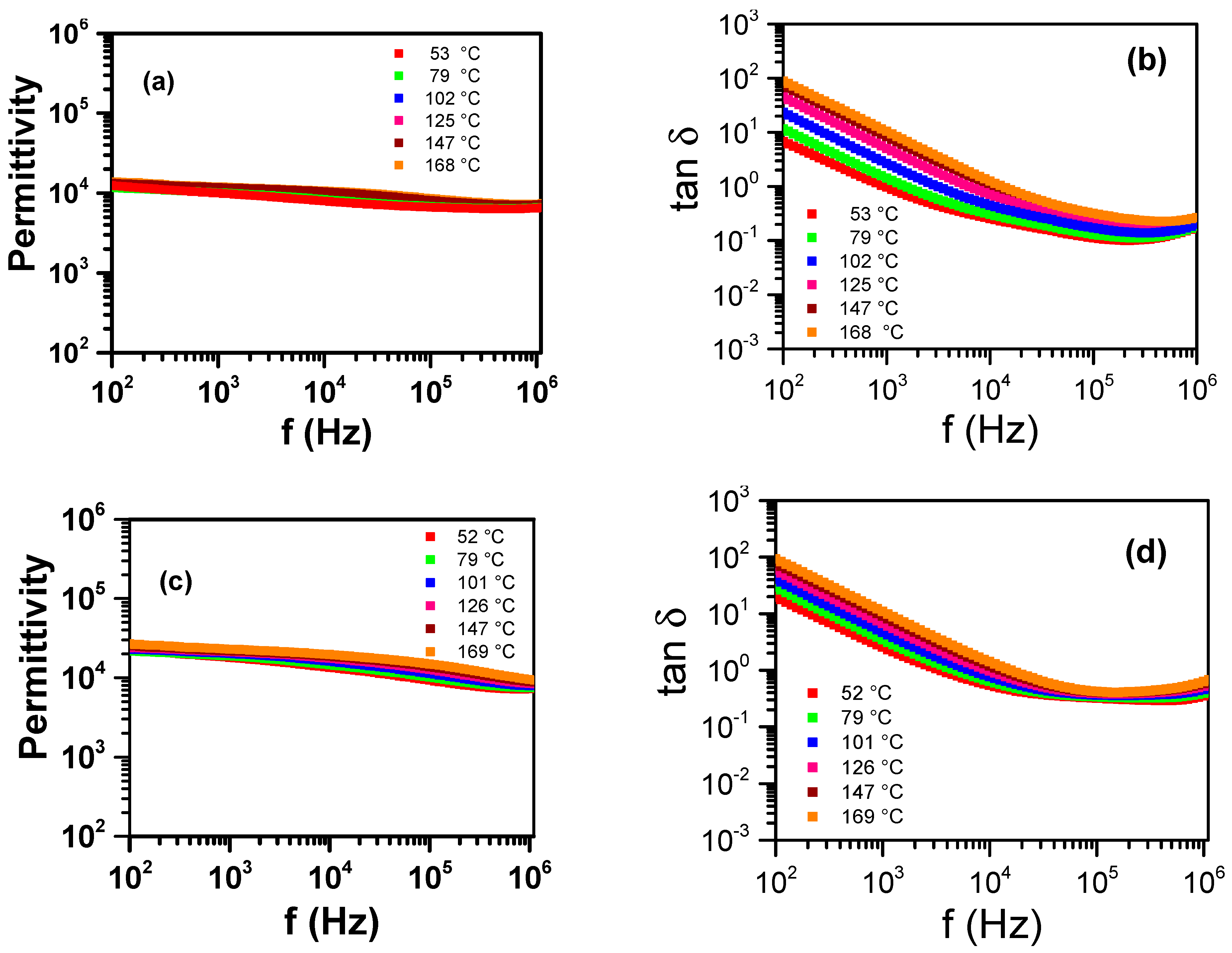
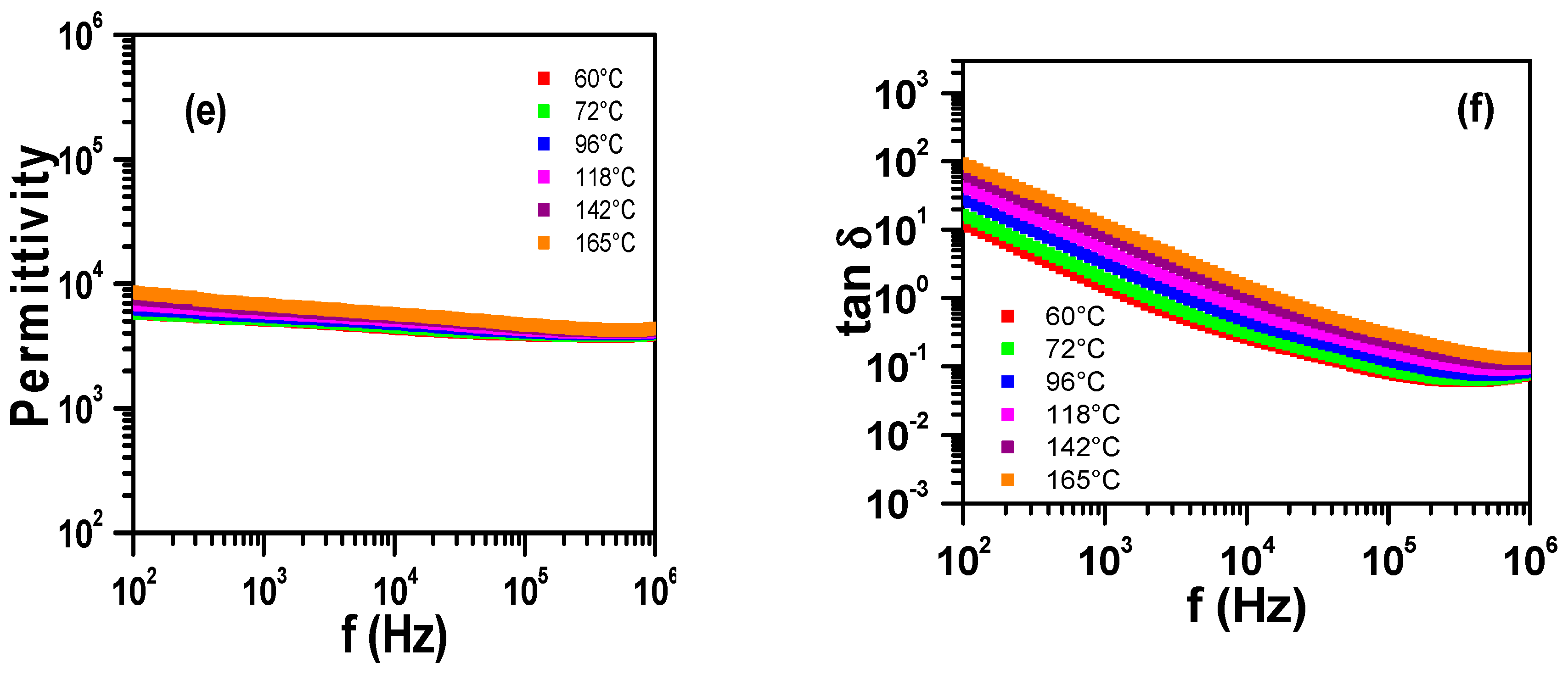
The stable configuration of TiO2 co-doped with Y3+ and Nb5+ was studied using the density functional theory (DFT) utilizing the Quantum Espresso (7.0 version) software. The ultrasoft pseudopotential wave (USPP) and the GGA-PBE (Perdew–Burke–Ernzerhof) methods were employed to describe the ionic potentials and exchange correlation energy of electrons, respectively. Supercells of 3 × 2 × 4 and 2 × 2 × 6 were created from the rutile cell. Several ab initio calculations of self-consistent field were performed with the PWscf package, with the energy varying in the 163.26 to 680.28 eV range, to evaluate the cutoff of the plane-wave. The optimized structures were observed with XCrysden (1.6.2-4 version) software.

3. Results

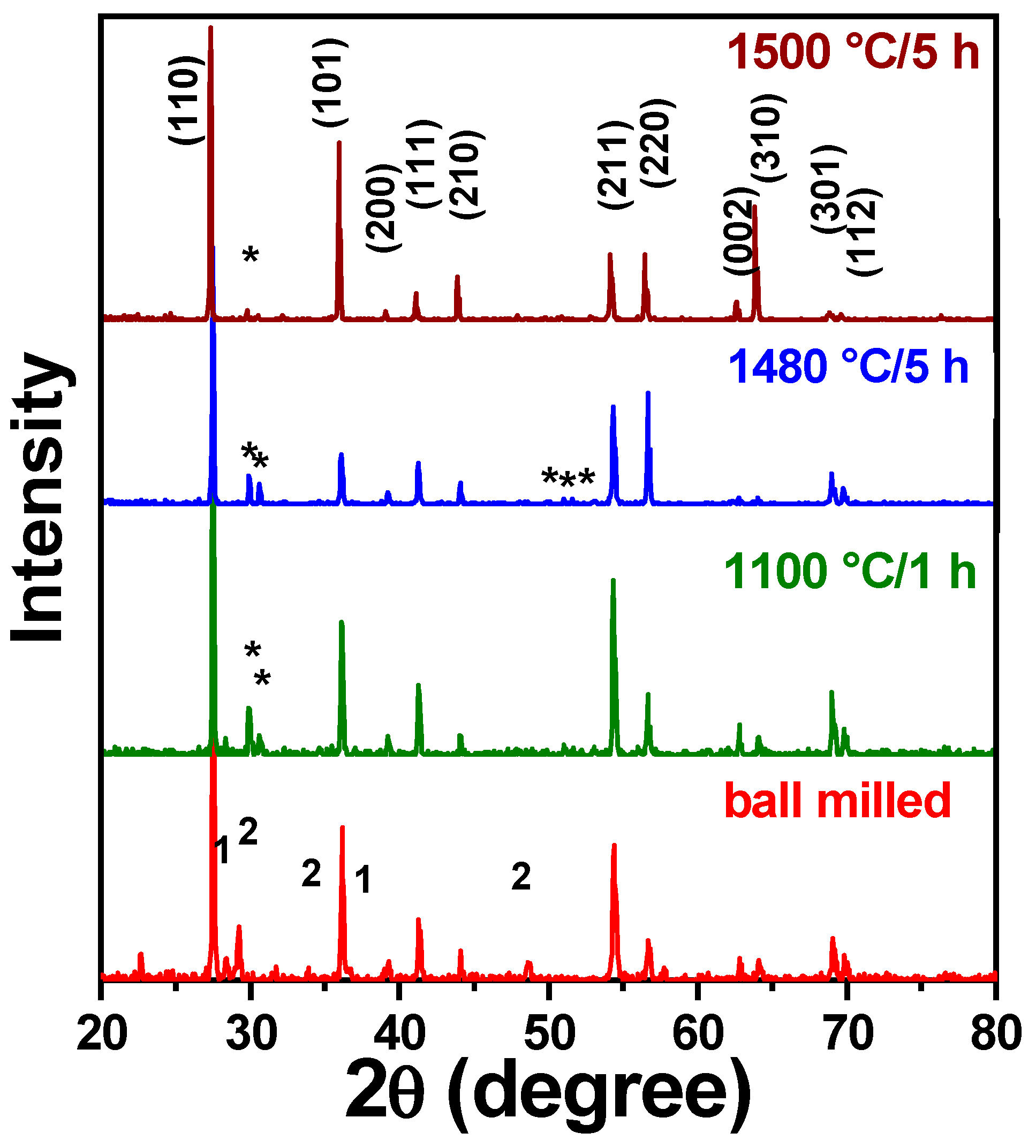
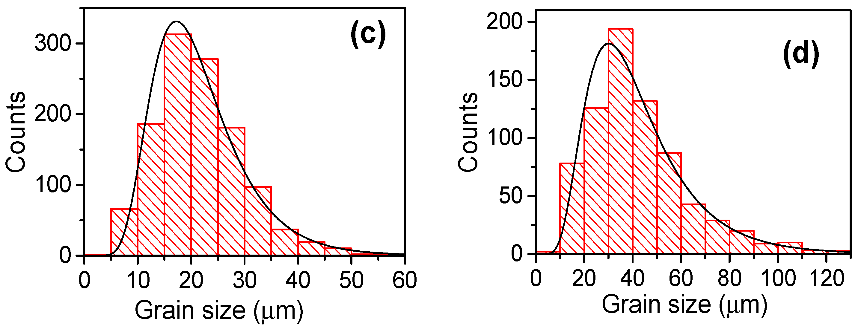
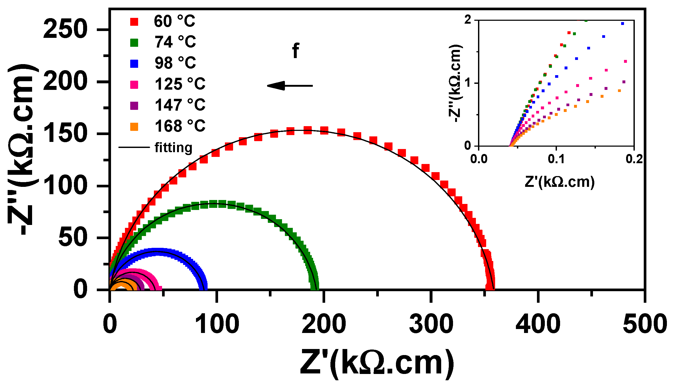
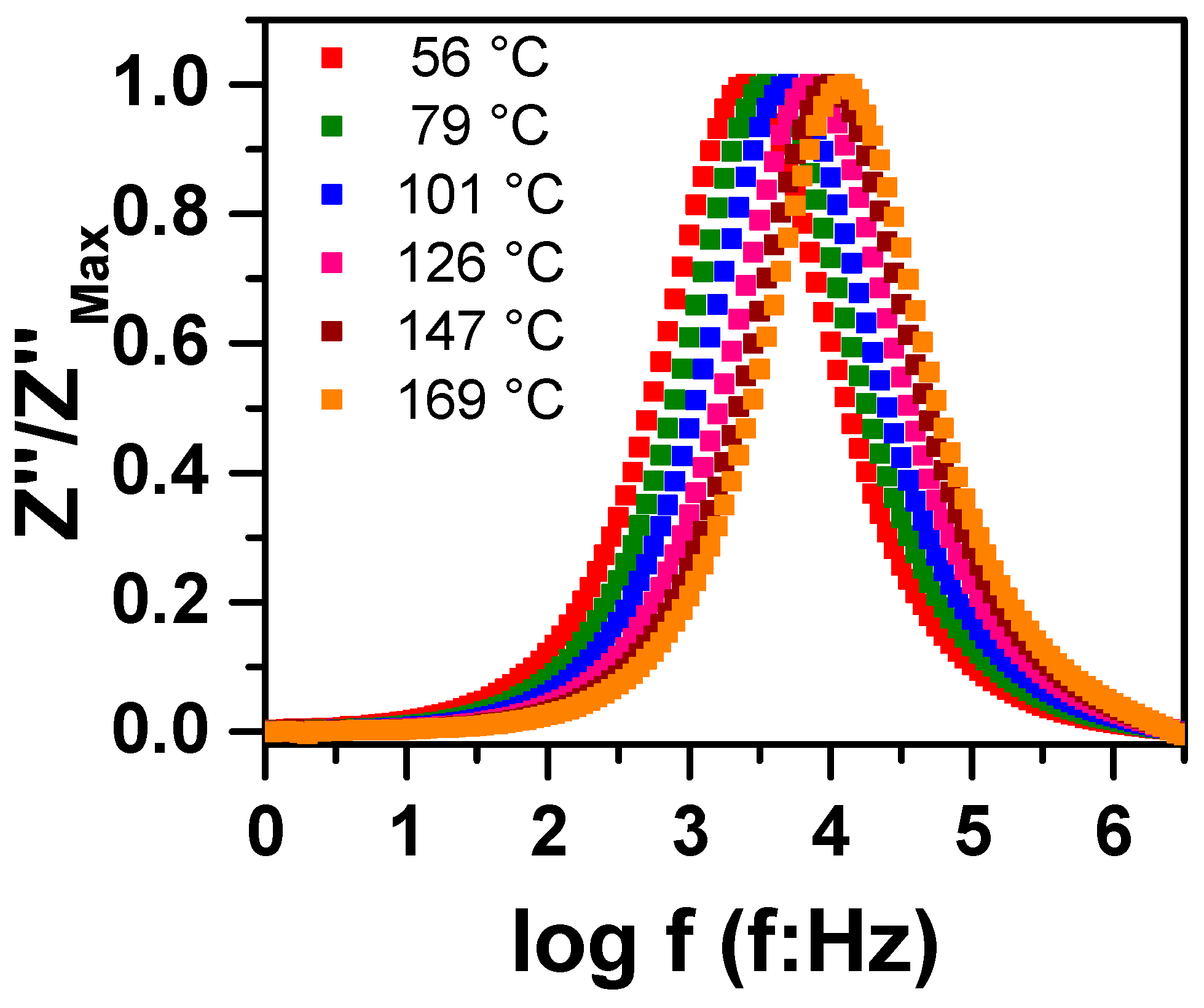
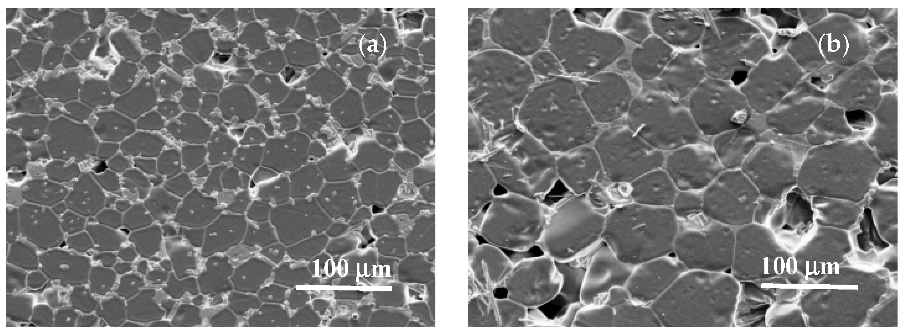
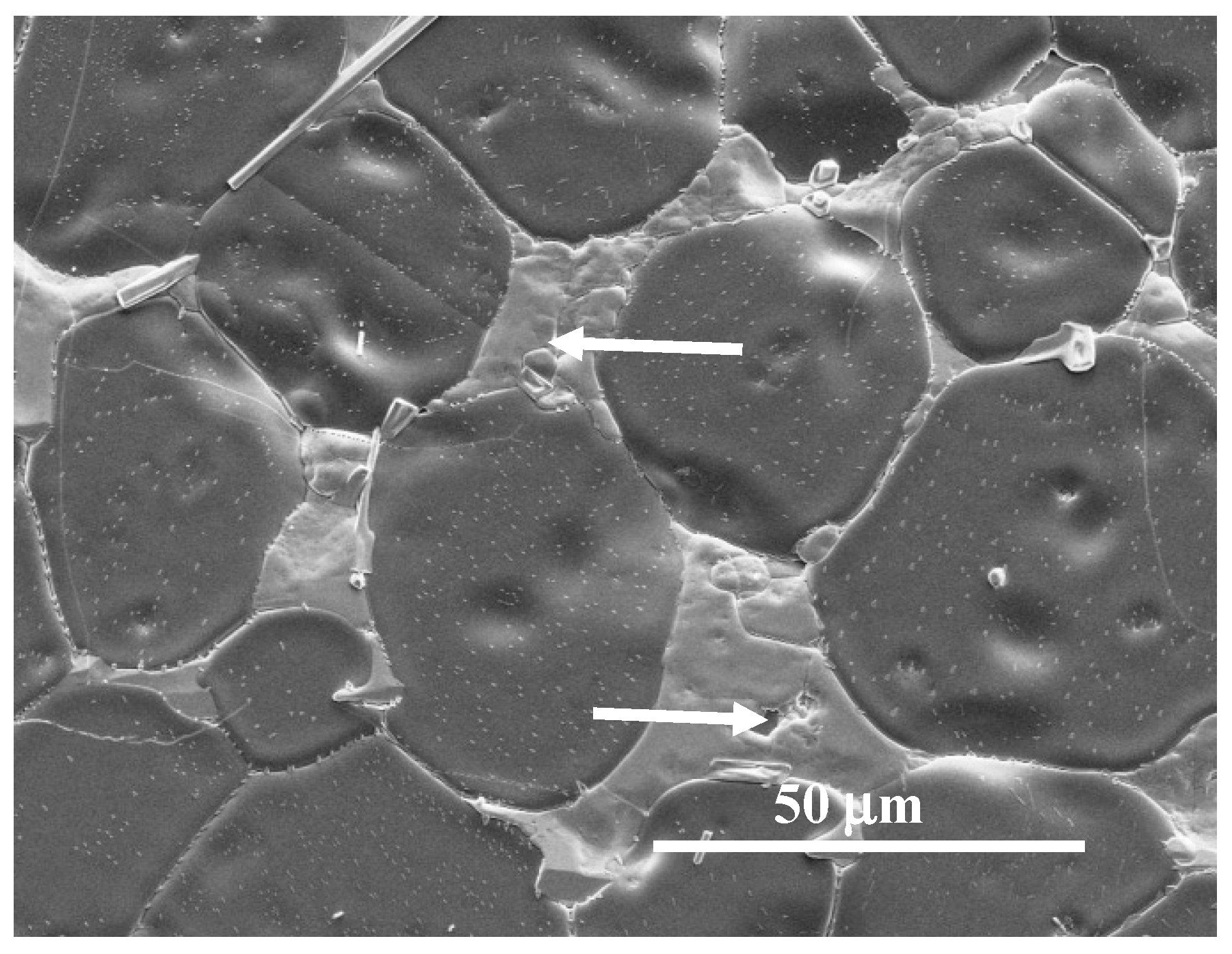
3.1. Sintering Temperature

Figure 1 depicts XRD patterns of YNTO10 mixed powders after wet ball milling and calcination, and of sintered pellets. The XRD profile of the milled powder exhibits, as expected, the characteristic peaks of the starting materials: TiO2 (indexed), Nb2O5 (1) and Y2O3 (2). The diffraction peaks of the powder calcined at 1100 °C match those of the tetragonal structure of rutile. Small intensity peaks, marked with *, are associated with a secondary phase, YNbTiO6 (PDF 83-1318). After sintering, the XRD patterns are essentially like that of the calcined powder, except for the peak intensity of the secondary phase that decreases with increasing sintering temperature. No other phases were detected under experimental uncertainties of the technique.
Typical microstructure features of sintered YNTO10 are shown in Figure 2. The specimen sintered at 1480 °C (Figure 2a) exhibits polygonal grains of varying sizes. In addition, small cubic- and prism-like grains are observed at grain boundaries and triple grain junctions, due to YNbTiO6 secondary phase. Moreover, nanosized rounded grains randomly distributed at the grain boundaries and on the surface of grains are observed. It was found by transmission electron microscopy that the solubility limit of yttrium in rutile was only ~0.1 mol%, and that the excess of dopant segregates at the grain boundaries [20]. Then, the observed nanosized grains may be related to free yttrium oxide, not detected in XRD experiments due to its low concentration and/or size. The increase in the sintering temperature to 1500 °C promoted grain growth, and the shape of the grains of the matrix turned to rounded (Figure 2b). The fraction of secondary phases at grain boundaries is comparatively small, in this case. The distributions of grain sizes shown in Figure 2c (1480 °C) and Figure 2d (1500 °C) are of log normal type. The grains of secondary phases were not considered in this analysis. The wider distribution of grain sizes of the specimen sintered at the highest temperature is remarkable. The mean grain sizes are listed in Table 1. It may be noted that the mean grain size of the specimen sintered at 1500 °C is almost twofold that of specimens sintered at 1480 °C.
Figure 3 shows a specific microregion of YNTO10 sintered at 1500 °C with high magnification. A light-gray color non-crystalline phase (indicated by arrows) spreading out the grain boundaries may be seen. This phase is barely observed in the micrographs of the specimens sintered at 1480 °C. These results evidence the relatively low solubility (<5 mol%) of both Y and Nb in the rutile matrix, leading to segregated secondary phases.
The increase in the sintering temperature by only 20 °C, from 1480 to 1500 °C, accelerated the grain growth, promoted a change in the shape of the grains, and yielded a non-crystalline phase at the grain boundaries. These effects seem to be a consequence of a change from solid-state to liquid-phase sintering mechanism. The origin of a liquid-phase during sintering of YNTO10 may be attributed to the closeness of the melting point of Nb2O5 (~1512 °C) and the sintering temperature, and to a relatively long sintering time.
To obtain better insight into the constitution of the non-crystalline phase, the elemental mapping of a selected microregion of the specimen sintered at 1500 °C is shown in Figure 4. The grains consist mostly of Ti, whereas the non-crystalline phase seems to contain primarily Nb and Y, as further evidence of the low solubility of these co-dopants in TiO2. The overall results indicate a complex microstructure evolution of TiO2 containing yttrium and niobium as a function of the sintering temperature, which may impact the dielectric properties of YNTO10.
The electrical measurements carried out by electrochemical impedance spectroscopy reveal a similar behavior of co-doped TiO2 specimens, independent of the sintering temperature. Hence, in this section, only results for specimens sintered at 1500 °C will be shown.
The dielectric properties of YNTO10 as a function of the frequency, measured at several temperatures, are depicted in Figure 5. Colossal permittivity values were obtained (≥103) over a wide range of frequencies. The electric permittivity decreases slowly with increasing frequency. The evolution of the dissipation factor with the frequency follows the same trend, achieving lower values at ~102 kHz. Values of ε′ and tan δ obtained for specimens sintered at different temperatures and measured at ~60 °C are summarized in Table 1. The electric permittivity increases with increasing sintering temperature, whereas the dissipation factor does not vary considerably.
Figure 6 shows the EIS plots in the complex plane [−Z′′(ω) × Z′(ω)] of YNTO10. The Z′′(ω) and Z′(ω) are the imaginary and real components of the impedance, respectively, and ω = 2πf is the relaxation frequency. These plots, recorded at several temperatures, were normalized for specimen dimensions for comparison purposes. The impedance spectroscopy plots consist of a single arc in the low frequency (≤103 Hz) range corresponding to the resistive and capacitive effects of the interfaces and grain boundaries (henceforward, these will be simply called interfaces). The diameter of the interface arc decreases with increasing temperature, due to ohmic conduction. The inset highlights the high-frequency region of the impedance diagrams, where the nonzero intercept is the electrical resistivity of the bulk. The very low resistivity of the bulk compared to that of the interfaces is noticeable. This type of EIS spectrum looks like that of CCTO with a low resistivity and semiconductor type bulk along with an insulating interface [21]. The shift of the high frequency intercept with the measuring temperature is sluggish. Then, the analysis of the EIS spectra was focused on the interface arc assumed to correspond to an equivalent electric circuit with a resistance in parallel with a constant phase element (CPE). The CPE represents the deviation from an ideal (Debye) capacitor behavior. The main parameters related to CPE are the pseudo capacitance Q and the index n reflecting the deviation from the ideal Debye behavior, such that
C = Q 1 / n R 2 ( 1 n ) n
where C is the capacitance and R 2 the interface resistance.
Table 1 summarizes C and n values obtained from fitting the experimental data. Differences in the capacitance values of YNTO10 sintered at different temperatures are attributed to the relatively large amount of the non-crystalline phase at grain boundaries in specimens sintered at 1500 °C. Lowering the sintering temperature leads to a near unity value of the index n, indicating a small deviation from the ideal capacitor behavior. Activation energy, Ea, values calculated from Arrhenius plots obtained from fitting the electrical conductivity data are also listed in Table 1 and correlate with previously determined values [19]. The activation energy values in the ~0.2 to ~0.3 eV range are much higher than that of the bulk, roughly estimated as 21 meV. Therefore, the microstructure of TiO2 co-doped with Y3+ and Nb5+ consists of semiconducting grains and low-conductivity interfaces, suggesting that the IBLC mechanism is, at least, partially responsible for the electrical behavior of this ceramic. Moreover, the secondary phases resulting from segregation of co-dopants contribute to the small increase in the electric permittivity and decrease in the dissipation factor (Table 1).
Figure 7a shows the evolution of the imaginary component of the total impedance [−Z″(ω)] as a function of the frequency. At 60 °C, a peak occurs at ~1 kHz, characterizing the relaxation of the interfaces. This peak shifts to higher frequencies with increases in the measuring temperature, revealing a thermally activated process. The frequency dependence of the complex electric modulus, M″, of YNTO10 sintered at 1500 °C is shown in Figure 7b. The complex electric modulus exhibits a peak with maximum amplitude in the same range as that of Z″, suggesting that the relaxation mechanism is related to long-range transport of charge carriers [22]. At high frequencies (>1 MHz) a second relaxation mechanism seems to occur, which is indicated by the rise in the complex modulus spectra. This second relaxation is related to the bulk of the ceramic. In the low-frequency limit, M″ tends to zero, highlighting a minor impact of the electrodes in the relaxation mechanism of YNTO10; thereby, a negligible influence of the SBLC mechanism may be advanced.

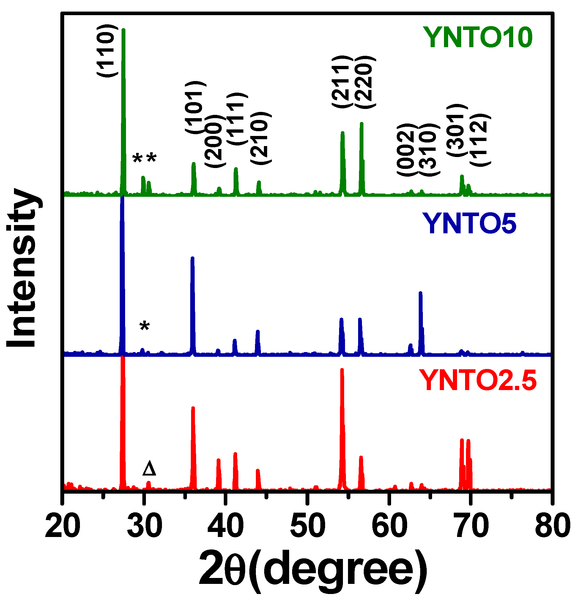
3.2. Concentration of Co-Dopants

The influence of the concentration of co-dopants on the properties of YNTO was investigated in specimens sintered at 1480 °C.
The XRD patterns of YNTO with different co-dopant contents are shown in Figure 8. The profile of YNTO10 is displayed here for comparison. The overall XRD patterns are like each other, with minor differences attributed to secondary phases. Specimens with total co-dopant contents of 0.05 and 0.10 show reflections of the YNbTiO6 phase (indicated with *). The concentration of this phase seems to increase with increasing the total concentration of co-dopants, apparently due to the limited solubility of these cations into the rutile lattice. The XRD pattern of YNTO2.5, in contrast, does not exhibit reflections of that secondary phase, but some of Y2Ti2O7 (PDF 87-1849), characteristics of the pyrochlore structure. This result indicates a high solubility of Nb5+ compared to Y3+ in the TiO2 matrix.
SEM micrographs of polished and etched surfaces of YNTO2.5 and YNTO5 are depicted in Figure 9. Polygonal grains of varying sizes are observed in both images.
The determined mean grain sizes are summarized in Table 1. It is noteworthy that the mean grain size of YNTO5 is larger than that of YNTO10 sintered at the same temperature. Then, the total co-dopant content incorporated into the crystal lattice of TiO2 and promoting grain growth is higher than x = 0.025, but lower than 0.10. The excess of co-dopants segregates at the grain boundaries and probably inhibits grain growth during sintering.
Figure 10 shows the frequency dependence of the electric permittivity (a, c and e) and dissipation factor (b, d and f) of YNTO2.5 (a,b), YNTO5 (c,d) and YNTO10 (e,f) measured at several temperatures. Colossal permittivity values, in the 103 to 104 range were obtained for all specimens. Those values varied slightly with both temperature of measurement and frequency. The value of ε′ increases with increasing content of co-dopants and it is maximum for YNTO5 (Table 1). Related to the sintering temperature, the electric permittivity is higher for specimens sintered at 1500 °C (Figure 5a) than at 1480 °C (Figure 10e). In contrast, specimens sintered at 1480 °C show enhanced temperature stability. The dissipation factor exhibits similar behavior for all specimens, decreasing with increasing frequency. The minimum value of the dissipation factor was obtained at approximately 102 kHz.
All sintered specimens display similar impedance plots. Figure S1 (Supplementary Materials) shows [−Z″(ω) × Z′(ω)] plots collected at several temperatures for YNTO5. The nonzero intercept at high frequencies (Figure S1 inset) corresponds to the bulk resistivity, whereas the intercept at low frequencies is related to the resistivity of interfaces. Fitting of EIS plots at several temperatures allowed for obtaining the Arrhenius plots of the electrical conductivity of YNTO specimens; thereby, the values of C, n and Ea were determined (Table 1). The capacitance of interfaces for YNTO5 is more than twice those of other compositions. The same occurs with the electric permittivity. In contrast, the dissipation factor is higher for YNTO5, whereas the index n does not vary considerably.
Figure 11 shows the frequency dependence of the normalized complex impedance, Z″/Z″MAX, of YNTO5. The single peak with maximum close to 1 kHz and characterizing the relaxation of interfaces shifts to higher frequencies with increasing temperature, similarly to specimens sintered at 1500 °C. The full width at half maximum (~1.4) is larger than that of the ideal Debye behavior (1.14), due to a distribution of relaxation time.

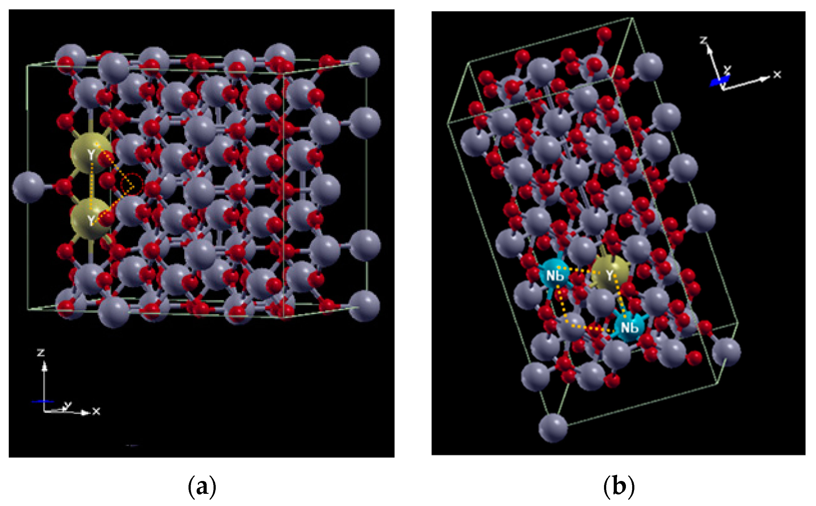
3.3. Computational Structural Modeling

Even though the experimental results point to the IBLC mechanism as dominant in the dielectric properties of YNTO, theoretical calculations were performed to evaluate the effects of the introduction of cations with dissimilar valences and sizes into the rutile lattice.
Figure S2 (Supplementary Materials) shows the initial structures of (a) rutile 3 × 2 × 4 supercell, (b) replacement of one Ti4+ for twoY3+ and one oxygen vacancy, (c) rutile 2 × 2 × 6 supercell, and (d) replacement of one Ti4+ for two Nb5+ and one Y3+.
The optimized structures after full relaxation through ab initio calculations showing the triangular and diamond defects are shown in Figure 12, and the parameters from DFT simulations and calculations are summarized in Table 2. Insertion of cations with different sizes and valences than those of Ti4+ promoted a redistribution of ions inside the rutile lattice and distortion of the bond angles of Ti ions neighboring the dopants. The lattice parameters are in general agreement with those calculated from X-ray diffraction patterns. The rutile lattice is distorted by doping with niobium and yttrium, with consequent increases in the a and c parameters, but the c/a ratio varies only slightly. The lattice angles also experience some deviation from 90°, indicating a tendency to change from tetragonal to orthorhombic structure. It is also noted that the Ti-O bond length decreases with the formation of defect clusters.
Analysis of the electronic structure was also carried out, and Figure S3 shows results for the density of states (DOS). The band gap energy increases by about 0.2 eV with the introduction of triangular- or diamond-type defects through substitutions into the rutile lattice.
The above results indicate that substantial changes are produced by defects in the crystal lattice of TiO2 co-doped with aliovalent cations. Despite the relatively low solubility of Y3+ and Nb5+ in the TiO2 matrix, their effects are not negligible, as evaluated by DFT calculations. Therefore, it is reasonable to assume that the dielectric properties of TiO2 co-doped with Y and Nb are due to both mechanisms, the EPDD acting on the bulk response and the IBLC at the interfaces.

4. Conclusions

Secondary phases were found to emerge at the grain boundaries of co-doped TiO2, due to the relatively low solubility of Y2O3 and Nb2O5 in the matrix. The content of the YNbTiO6 secondary phase decreases with increasing sintering temperature. The relatively low melting point of Nb2O5 favors the liquid-phase mechanism during sintering at 1500 °C. An increase in the mean grain size in sintered co-doped TiO2 was acquired, either by tuning the total amount of co-dopants or by increasing the sintering temperature; the former allowed for achieving higher electric permittivity, whereas the low dissipation factor was obtained with the latter. DFT calculations showed that significant changes in the crystal lattice and band gap of TiO2 occur with Y3+ and Nb5+ co-doping.

Supplementary Materials

The following supporting information can be downloaded at: https://www.mdpi.com/article/10.3390/ceramics7010026/s1, Figure S1. EIS spectra of YNTO5 sintered at 1480 °C. Inset: high frequency region.; Figure S2. Structures of (a) rutile 3 × 2 × 4 supercell, (b) substitution of one Ti for two Y and one oxygen vacancy, (c) rutile 2 × 2 × 6 supercell, and (d) substitution of Ti for two Nb and one Y.; Figure S3. Density of states (DOS) of (a) rutile 3 × 2 × 4 supercell, (b) substitution of one Ti for two Y and one oxygen vacancy, (c) rutile 2 × 2 × 6 supercell, and (d) substitution of Ti for two Nb and one Y.

Author Contributions

Conceptualization, E.N.S.M.; methodology, E.N.S.M. and D.Y.B.S.; software, D.Y.B.S.; validation and formal analysis, D.Y.B.S. and E.N.S.M.; resources, R.M. and E.N.S.M.; writing—original draft preparation, E.N.S.M. and R.M.; writing—review and editing, E.N.S.M. and R.M.; supervision, E.N.S.M. All authors have read and agreed to the published version of the manuscript.

Funding

The authors acknowledge financial supports from FAPESP (Proc. 2013/07692-2), CNPq (Proc. 305557/2022-0, 302357/2018-1), CAPES (Finance code 0001) and CNEN.

Institutional Board Review Statement

Not applicable.

Informed Consent Statement

Not applicable.

Data Availability Statement

The data presented in this study are available on reasonable request from the corresponding author.

Acknowledgments

The authors acknowledge A. P. Suaide from the University of São Paulo, for providing computational resources.

Conflicts of Interest

The authors declare no conflict of interest.

References

  1. Buchanan, R.C. Ceramic Materials for Electronics; CRC Press: Boca Raton, FL, USA, 2018; ISBN 978-0-8247-4028-3. [Google Scholar]
  2. Li, J.; Cho, K.; Wu, N.; Ignatiev, A. Correlation between dielectric properties and sintering temperatures of polycrystalline CaCu3Ti4O12. IEEE Trans. Dielectr. Electr. Insul. 2004, 11, 534–541. [Google Scholar] [CrossRef]
  3. Krohns, S.; Lunkenheimer, P.; Meissner, S.; Reller, A.; Gleich, B.; Rathgeber, A.; Glauger, T.; Buhl, H.U.; Sinclair, D.C.; Loidl, A. The route to resource-efficient novel materials. Nat. Mater. 2011, 10, 899–901. [Google Scholar] [CrossRef] [PubMed]
  4. Guillemet-Fritsch, S.; Valdez-Nava, Z.; Tenailleau, C.; Lebey, T.; Durand, B.; Chane-Ching, J.Y. Colossal permittivity in ultrafine grain size BaTiO3−x and Ba0.95La0.05TiO3−x materials. Adv. Mater. 2008, 20, 551–555. [Google Scholar] [CrossRef]
  5. Wu, J.; Nan, C.W.; Lin, Y.; Deng, Y. Giant dielectric permittivity observed in Li and Ti doped NiO. Phys. Rev. Lett. 2002, 89, 217601. [Google Scholar] [CrossRef] [PubMed]
  6. Zhang, L.; Tang, Z.J. Polaron relaxation and variable-range-hopping conductivity in the giant-dielectric-constant material CaCu3Ti4O12. Phys. Rev. B 2004, 70, 174306. [Google Scholar] [CrossRef]
  7. Bak, T.; Nowotny, J.; Rekas, M.; Sorrell, C. Defect chemistry and semiconducting properties of titanium dioxide: II Defect diagrams. J. Phys. Chem. Solids 2003, 64, 1057–1067. [Google Scholar] [CrossRef]
  8. Bonkerud, J.; Zimmermann, C.; Weiser, P.M.; Vines, L.; Monakhov, E.V. On the permittivity of titanium dioxide. Sci. Rep. 2021, 11, 12443. [Google Scholar] [CrossRef]
  9. Hu, W.; Liu, Y.; Withers, R.L.; Frankcombe, T.J.; Norén, L.; Snashall, A.; Kitchin, M.; Smith, P.; Gong, B.; Chen, H.; et al. Electron-pinned defect-dipoles for high-performance colossal permittivity materials. Nat. Mater. 2013, 12, 821–826. [Google Scholar] [CrossRef]
  10. Dong, W.; Hu, W.; Berlie, A.; Lau, K.; Chen, H.; Withers, R.L.; Liu, Y. Colossal dielectric behavior of Ga+Nb co-doped rutile TiO2. Appl. Mater. Interfaces 2015, 7, 25321–25325. [Google Scholar] [CrossRef]
  11. Peng, H.; Liang, P.; Zhou, X.; Peng, Z.; Xiang, Y. Good thermal stability giant permittivity, and low dielectric loss for X9R-type (Ag1/4Nb3/4)0.005Ti0.995O2 ceramics. J. Am. Ceram. Soc. 2019, 102, 970–975. [Google Scholar] [CrossRef]
  12. Nachaithong, T.; Moontragoon, P.; Chanlek, N.; Thongbai, P. Fe3+/Nb5+ co-doped rutile-TiO2 nanocrystalline powders prepared by a combustion process: Preparation and characterization and their giant dielectric response. RSC Adv. 2020, 10, 24784–24794. [Google Scholar] [CrossRef] [PubMed]
  13. Zhou, L.; Peng, Z.; Zhu, J.; Shi, Q.; Liang, P.; Chao, X.; Yang, Z. High temperature stability and low dielectric loss in colossal permittivity TiO2 based ceramics co-doped with Ag+ and Mo6+. Mater. Chem. Phys. 2023, 295, 127072. [Google Scholar] [CrossRef]
  14. Wang, Z.; Li, Y.; Chen, H.; Fan, J.; Wang, X.; Ma, X. Correlation between the radius of acceptor ion and the dielectric properties of co-doped TiO2 ceramics. Ceram. Int. 2019, 45, 14625–14633. [Google Scholar] [CrossRef]
  15. Wang, W.; Li, L.; Lu, T.; Zhang, N.; Luo, W. Multifarious polarization in high-performance colossal permittivity titanium dioxide ceramics. J. Alloys Compd. 2019, 806, 89–98. [Google Scholar] [CrossRef]
  16. Hu, W.; Lau, K.; Liu, Y.; Withers, R.L.; Chen, H.; Fu, L.; Gong, B. Colossal dielectric permittivity in (Nb + Al) codoped rutile TiO2 ceramics: Compositional gradient and local structure. Chem. Mater. 2015, 27, 4934–4942. [Google Scholar] [CrossRef]
  17. Tuichai, W.; Danwittayakul, S.; Chanlek, N.; Thongbai, P. Effects of the sintering temperature on microstructure and giant dielectric properties of (V + Ta) co-doped TiO2 ceramics. J. Alloys Compd. 2017, 725, 310–317. [Google Scholar] [CrossRef]
  18. Nachaithong, T.; Tuichai, W.; Kidhhunthod, P.; Chanlek, N.; Thongbai, P.; Maensiri, S. Preparation, characterization, and giant dielectric permittivity of (Y3+ and Nb5+) co-doped TiO2 ceramics. J. Eur. Ceram. Soc. 2017, 37, 3521–3526. [Google Scholar] [CrossRef]
  19. Wang, X.; Zhang, B.; Xu, L.; Wang, X.; Hu, Y.; Shen, G.; Sun, L. Dielectric properties of Y and Nb co-doped TiO2 ceramics. Sci. Rep. 2017, 7, 8517. [Google Scholar] [CrossRef]
  20. Wang, Q.; Lian, G.; Dickey, E.C. Grain boundary segregation in yttrium-doped polycrystalline TiO2. Acta Mater. 2004, 52, 809–820. [Google Scholar] [CrossRef]
  21. Porfírio, T.C.; Muccillo, E.N.S. Effects of LiF addition on microstructure and dielectric properties of CaCu3Ti4O12 ceramics. Ceram. Int. 2016, 42, 12005–12009. [Google Scholar] [CrossRef]
  22. Gerhardt, R. Impedance and dielectric spectroscopy revisited: Distinguishing localized relaxation from long-range conductivity. J. Phys. Chem. Solids 1994, 55, 1491–1506. [Google Scholar] [CrossRef]
Figure 1. XRD patterns of YNTO10 mixed powders after wet ball milling and calcination, and of sintered pellets. 1—Nb2O5, 2—Y2O3, *—YNbTiO6.
Ceramics 07 00026 g001
Figure 2. SEM micrographs (a,b) and grain size distribution (c,d) of YNTO10 sintered at (a,c) 1480 °C and (b,d) 1500 °C.
Ceramics 07 00026 g002aCeramics 07 00026 g002b
Figure 3. High-magnification SEM micrograph of a selected microregion of YNTO10 sintered at 1500 °C. A secondary phase is indicated by arrows.
Ceramics 07 00026 g003
Figure 4. SEM micrograph (top left) and elemental mapping of a selected microregion of YNTO10 sintered at 1500 °C.
Ceramics 07 00026 g004
Figure 5. Frequency dependence of the (a) electric permittivity and (b) dissipation factor of YNTO10 sintered at 1500 °C and measured at several temperatures.
Ceramics 07 00026 g005
Figure 6. EIS spectra of YNTO10 sintered at 1500 °C. Inset: high-frequency region.
Ceramics 07 00026 g006
Figure 7. Frequency dependence of (a) imaginary impedance and (b) complex modulus of YNTO10 sintered at 1500 °C.
Ceramics 07 00026 g007
Figure 8. XRD patterns of YNTOx, x = 0.025, 0.050 and 0.10 sintered at 1480 °C. ∆—Y2Ti2O7, *—YNbTiO6.
Ceramics 07 00026 g008
Figure 9. SEM micrographs of (a) YNTO2.5 and (b) YNTO5 sintered at 1480 °C.
Ceramics 07 00026 g009aCeramics 07 00026 g009b
Figure 10. Frequency dependence (a,c,e) of the electric permittivity and (b,d,f) dissipation factor of YNTO2.5 (a,b), YNTO5 (c,d) and YNTO10 (e,f) sintered at 1480 °C and measured at several temperatures.
Ceramics 07 00026 g010aCeramics 07 00026 g010b
Figure 11. Frequency dependence of the normalized complex impedance of YNTO5.
Ceramics 07 00026 g011
Figure 12. Crystalline structure of rutile with (a) triangular and (b) diamond defects.
Ceramics 07 00026 g012
Table 1. Values of the mean grain size (G), capacitance (C), n index, and activation energy (Ea) of interfaces, electric permittivity, and dissipation factor in YNTO sintered at 1480 °C and 1500 °C.
ParameterYNTO2.5YNTO5YNTO10YNTO10
(1480 °C)(1480 °C)(1480 °C)(1500 °C)
G (μm)18.8 ± 0.137.1 ± 0.120 ± 0.137.9 ± 0.2
ε′ (@ ~60 °C/10 kHz)794613,49944105490
tan δ (@ ~60 °C/10 kHz)0.260.540.270.21
n0.92 ± 0.010.90 ± 0.020.94 ± 0.010.85 ± 0.05
C (nF)3.1 ± 0.17.0 ± 0.52.1 ± 0.153.3 ± 0.5
Ea (eV)0.31 ± 0.050.19 ± 0.050.27 ± 0.050.33 ± 0.05
Table 2. Values of lattice parameters, bond angle and Ti-O bond length calculated by DFT, and lattice parameters determined by X-ray diffraction for YNTO sintered at 1480 °C.
a,b (Å)c (Å)c/aα (°)β (°)γ (°)Ti-O (Å)
3 × 2 × 44.6122.9600.6429090901.965
triangular4.6382.9810.643909090.241.953
2 × 2 × 64.6212.9540.6399090901.965
diamond4.6432.9910.64489.9889.9889.961.963
YNTO2.54.6042.9610.643----
YNTO54.6042.9630.643----
YNTO104.6042.9650.644----
Disclaimer/Publisher’s Note: The statements, opinions and data contained in all publications are solely those of the individual author(s) and contributor(s) and not of MDPI and/or the editor(s). MDPI and/or the editor(s) disclaim responsibility for any injury to people or property resulting from any ideas, methods, instructions or products referred to in the content.

