Article

Thermoelectric Properties of Si-Doped In2Se3 Polycrystalline Alloys

Department of Materials Science and Engineering, University of Seoul, Seoul 02504, Korea
*
Author to whom correspondence should be addressed.
These authors contributed equally to this work.
Ceramics 2022, 5(3), 281-287; https://doi.org/10.3390/ceramics5030022
Submission received: 30 April 2022 / Revised: 8 June 2022 / Accepted: 4 July 2022 / Published: 9 July 2022
(This article belongs to the Special Issue Advances in Ceramics)

Abstract

:
Post-metal chalcogenides, including InSe, In2Se3, and In4Se3, have attracted considerable attention as potential thermoelectric materials because of their intrinsically low thermal conductivity, which is attributed to their layered structure with weak van der Waals bonds. In this study, we examined the electrical and thermoelectric properties of Si-doped In2Se3 (In2−xSixSe3, x = 0, 0.005, 0.01, 0.015, and 0.02) polycrystalline samples. Hexagonal α(2H)-In2Se3 phase was synthesized without any impurity, and gradual changes in the lattice parameters were observed with Si doping. Drastic changes were observed for the measured electrical and thermal transport properties at 450–500 K, due to the phase transition from α to β at 473 K. The highest power factors were achieved by the sample with x = 0.015 for both α and β phases, exhibiting the values of 0.137 and 0.0884 mW/mK2 at 450 and 750 K, respectively. The total thermal conductivities of the α phase samples decreased gradually with increasing Si doping content, which is attributed to the point defect phonon scattering by Si doping. The total thermal conductivities of the β phase samples significantly decreased compared to those of the α phase samples. Therefore, the sample with x = 0.015 (In1.985Si0.015Se3) showed the maximum thermoelectric figure of merit values of 0.100 and 0.154 at 450 and 750 K, which are enhanced by 152 and 48% compared with those of the undoped α- and β-In2Se3 samples, respectively.

1. Introduction

Post-transition metal chalcogenides (PTMCs), such as Ga-, In-, and Sn-based semiconductors, have been studied in various fields. Primarily, PTMCs have been extensively investigated for transistors, photodetectors, solar cells, and thermoelectric materials [1,2,3]. In particular, the layered structure of most PTCMs facilitates them as thermoelectric materials; this is because the layered structure has a weak van der Waals bonding between the layers. Therefore, PTMCs have poor thermal transport properties, which indicates that they can be promising thermoelectric materials. Furthermore, thermoelectric technology directly converts temperature gradients into electrical potential, which facilitates the utilization of large amounts of waste heat from industries and automobiles, creating the potential for sustainable energy harvesting technologies [4,5]. The performance of thermoelectric materials is evaluated using dimensionless figure of merit, zT = S2σT/κtot, where S, σ, κtot and T are the Seebeck coefficient, electrical conductivity, total thermal conductivity, and absolute temperature, respectively. Herein, zT can be improved by increasing power factor (PF = S2σ) or decreasing κtot. However, this approach is complex because S and σ exhibit a trade-off relationship [6]. In addition, as σ increases, κtot also increases, because κtot can be expressed as κtot = κelec + κlatt, where κelec and κlatt are the electronic thermal conductivity and lattice thermal conductivity, respectively. The κelec is determined by the Wiedemann–Franz law (κelec = LσT, where L is the Lorentz number) [7]. Therefore, in recent years, the strategies of enhancing power factor and reducing the κlatt have been studied [8,9]. The effective use of various scattering mechanisms is important because the κlatt is inversely proportional to the phonon scattering [9,10,11].
To improve a zT, doping strategy has been actively applied to thermoelectric PTMCs. In the case of InSe, a zT for Si-doped InSe was improved to 0.18 (approximately by 210%) at 795 K, compared to pristine InSe [12]. Furthermore, a zT of 0.62 was observed for SnSe1.98Br0.02 at 750 K, which is 50% higher than that for pristine SnSe2 [13]. Rhyee et al. reported a zT of 1.48 for In4Se3−x at 705 K and a low thermal conductivity of ~0.74 Wm−1 K−1 [14]. Qian et al. reported a maximum zT of 1.35 for Ca-doped SnTe at 873 K [15]. To enhance zT of materials effectively, enhancing the effective mass, m*, reducing κlatt, and selecting the appropriate dopant are essential [16,17].
In2Se3, one of the PTMCs, has two primary phases, α and β. The α and β phases are stable below 473 K and above 473 K, respectively, and both of them have a layered structure [18,19]. Owing to this structural characteristic, they have low thermal conductivities. Indeed, the α phase has two crystal structures: hexagonal (2H) and rhombohedral (3R) [20,21,22,23]. The α(2H) phase is stable and α(3R) phase is unstable at room temperature. The complex phase change in In2Se3 may imply larger possibility of the intrinsic defects [23]. To synthesize a stable α(2H) phase, quenching process is necessary.
We investigated the effect of Si doping on the thermoelectric transport behavior of In2Se3. A series of In2−xSixSe3 (x = 0, 0.005, 0.01, 0.015, and 0.02) polycrystalline samples were synthesized and their electrical and thermal transport properties were analyzed. The zT were calculated to determine the optimum compositions for thermoelectric materials in Si-doped In2Se3.

2. Experimental Method

A series of In2−xSixSe3 compositions with nominal x = 0, 0.005, 0.01, 0.015 and 0.02 were synthesized via the conventional solid-state reaction in a vacuum-sealed quartz tube. High purity elements, In (99.999%, pellet), Si (99.999%, pellet), and Se (99.999%, pellet), were weighed with stoichiometric compositions. The loaded quartz ampules were heated at 1273 K for 10 h. In addition, pure α(2H) phases were obtained by quenching in ice water. The synthesized α(2H)-In2−xSixSe3 ingots were pulverized into powder using high-energy ball milling (SPEX 8000D, SPEX). All powders were densified via spark plasma sintering (SPS, SPS-1030, Sumitomo Coal Mining Co., Ltd., Tokyo, Japan) by heating at 923 K for 2 min at a pressure of 70 MPa. During sintering, the inside of the SPS chamber was kept under a vacuum (~10−5 Torr). Structural analysis of the powders was performed using X-ray diffraction (XRD, D8 Discover, Bruker) at 40 kV and 40 mA. Cu Kα radiation (λ = 1.5406 Å) and a scan rate of 0.02° s−1 were used to record patterns in the 2θ range of 20°–80°. Subsequently, the lattice parameter was calculated for each synthesized sample.The thermoelectric transport properties (S and σ) were simultaneously measured in the temperature range of 300–750 K using a thermoelectric property measurement system (ZEM-3, Advanced-Riko, Yokohama, Japan) in a He atmosphere along parallel direction of the SPS pressing direction, and the PF was calculated by measured S and σ. Hall measurement was performed in a Van der Pauw configuration at 300 K using a Hall measurement system (HMS5300, Ecopia) in the same direction. Furthermore, κtot was calculated using the relationship, κtot = ρsCpλ, where ρs, Cp and λ are the sample density, heat capacity, and thermal diffusivity, respectively, and ρs is the theoretical density of the α- and β-phases of In2Se3. Cp was measured using a differential scanning calorimeter (DSC8000, Perkin Elmer, Waltham, USA) in the temperature range of 273–473 K, and the measured values at 300 K and 473 K were used for the α and β phases, respectively. The measured Cp by differential scanning calorimetry (DSC) was shown in Figure S1 in Supplementary Information. λ was measured using the laser flash method (LFA457, Netzsch, Selb, Germany) in the temperature range of 300–750 K along SPS pressing direction so the zT can be calculated appropriately. The zT was evaluated based on the measured data. Energy-dispersive spectroscopy (EDS) by scanning electron microscopy (SEM) was performed for In2−xSixSe3 with nominal x = 0.01 and 0.02 to verify the existence of Si dopants (See Figure S2 and Table S1 in Supplementary Materials).

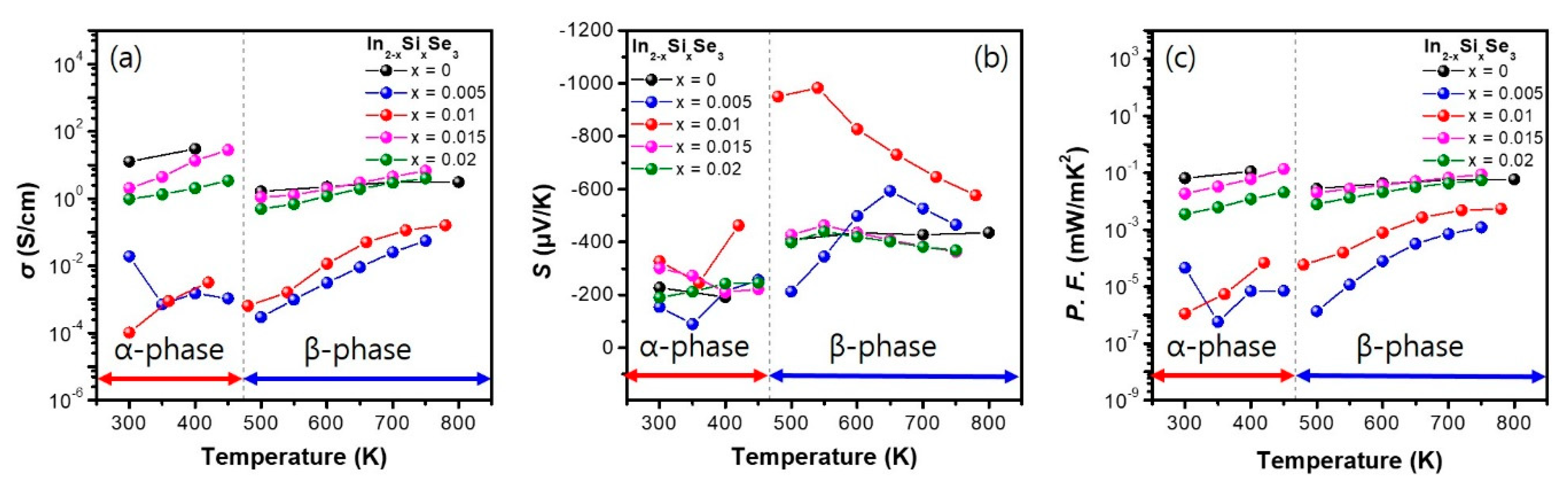
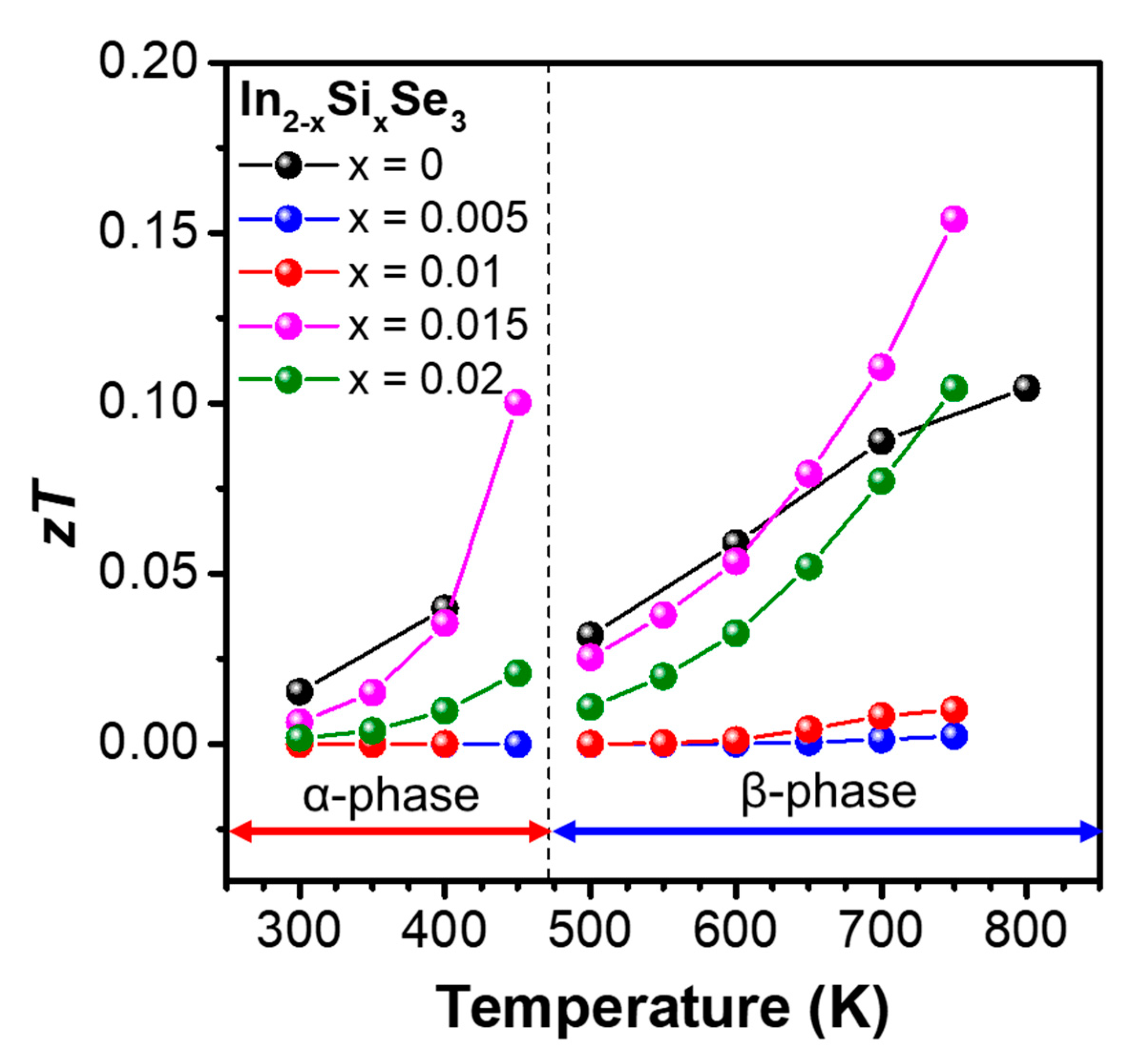
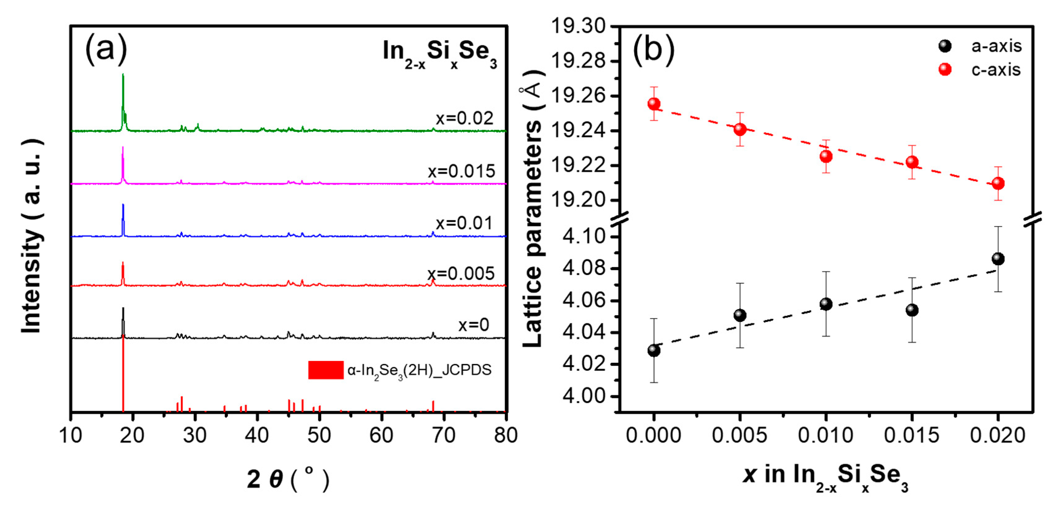
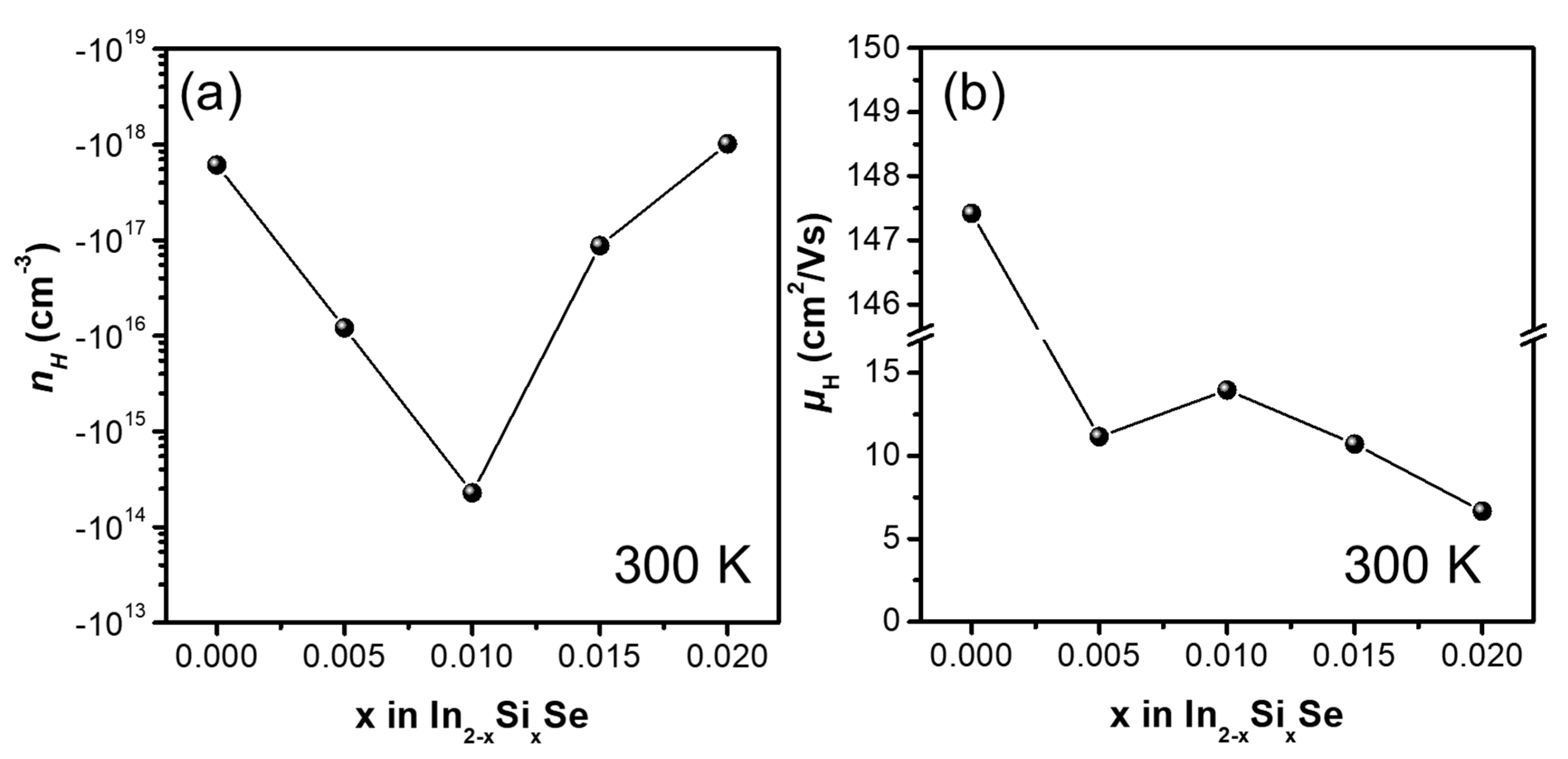
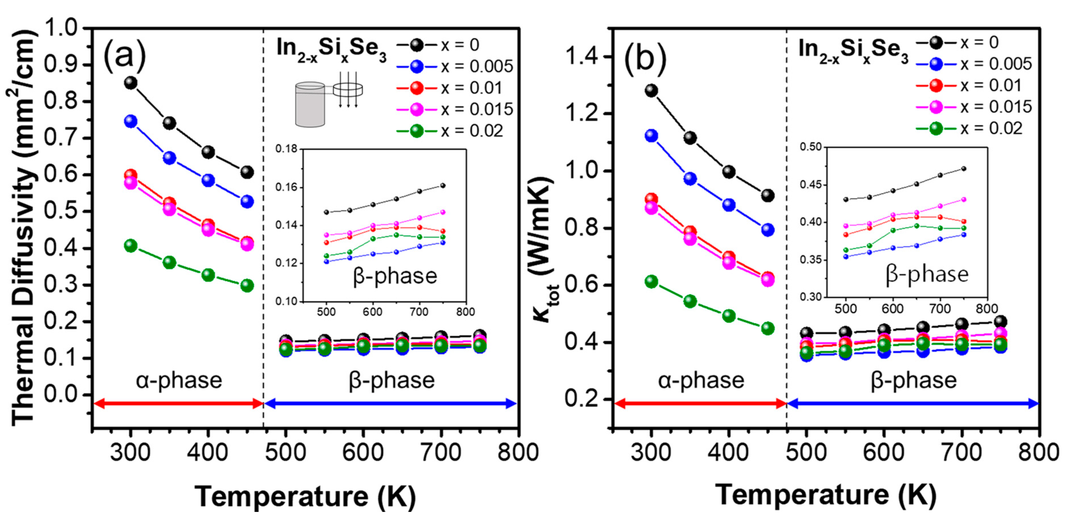
3. Results and Discussion

Figure 1a shows the XRD patterns of the synthesized Si-doped In2Se3. A series of In2−xSixSe3 samples were successfully synthesized as a α(2H) phase. Figure 2b shows the lattice parameters, which were calculated using the (004) and (102) diffraction peaks. The lattice parameter a gradually increases from 4.03 to 4.09 Å with increasing Si content. In contrast, the lattice parameter c gradually decreases from 19.3 to 19.2 Å. A gradual decrease in lattice parameter c can be explained by the fact that the ionic size of Si4+ is 54 pm, which is smaller than that of In3+ (94 pm), even though the modest increase in the lattice parameter a was seen. This unusual opposite change in lattice parameters was also seen in Si-doped InSe compounds [12]. However, these gradual changes of the lattice parameters indicate that Si is successfully substituted at the In sites. Additionally, Table 1 shows the atomic percentage directly measured by EDS-SEM for In2−xSixSe3 with x = 0.01 and 0.02.
Figure 2a,b show the plotted σ and S values of the In2−xSixSe3 (x = 0, 0.005, 0.01, 0.015, and 0.02) samples with different x values, measured using ZEM-3. The σ of all the samples decreased significantly during the α-β phase transition. The σ values at 450 K for the In2−xSixSe3 samples with x = 0, 0.005, 0.01, 0.015 and 0.02 were 30.3, 0.00108, 0.00322, 28.0 and 3.42 S/cm, respectively, and at 500 K, the σ values decreased to 3.11, 3.01 × 10⁻⁴, 6.47 × 10⁻⁴, 1.10 and 0.497 S/cm, respectively. Generally, the σ exhibited semiconductor behavior in both the α and β phases. The highest σ value for α phase was 30.30 S/cm for x = 0 at 400 K, and that for β phase was 6.705 S/cm for x = 0.015 at 750 K. Along with the σ, the magnitude of S values of the samples increased due to the phase transition at 500 K. The largest |S| values for both α and β phases were observed for the sample with x = 0.01; the value of S of the sample with x = 0.01 was −465.3 μV/K at 400 K and −950.4 μV/K at 500 K.
Figure 2c shows the calculated PF of the In2−xSixSe3 samples based on the measured σ and S. The PF gradually increased with increasing temperature in both the α and β phases. For all the samples, the PF decreased during the phase transition from α to β, which is mainly attributed to decreases in the σ. The maximum PF for the α phase samples was 0.137 mW/mK2 for x = 0.015 at 450 K, and that for the β phase samples was 0.0884 mW/mK2 for x = 0.015 at 750 K. Another phase transition from β phase to γ phase was reported in literature at ~ 620 K, however, the abrupt change of electrical transport properties was not seen in the experiment [23].
For better understanding of the electrical transport properties, Hall carrier concentration (nH) and Hall mobility (μH) were measured and are shown in Figure 3a and Figure 3b, respectively. The nH values of the samples were –6.10 × 10¹⁷, –1.21 × 10¹⁶, –2.27 × 10¹⁴, –8.78 × 10¹⁶, and −1.02 × 1018 cm−3 for x = 0, 0.005, 0.01, 0.015, and 0.02, respectively. The nH values of the samples decreased up to x = 0.01 and then increased to the largest value beyond x = 0.01, which seems to be abnormal. At this stage, the clear reason for this abnormal behavior is unknown, but it can be speculated that the various intrinsic defects, including vacancies, interstitials, and antisite defects, in In2Se3, seem to play complex roles as doping increases. Various intrinsic defects exist for this complex structure of α(2H)-In2Se3 [24]. The complex phase change in In2Se3 may imply larger possibility of the intrinsic defects [19,20,21,22,23]. In Figure 3b, the μH of all the doped samples decreased significantly, compared to pristine sample of x = 0. The μH of the sample with x = 0 was 147 cm2/Vs, whereas the μH of the samples with x = 0.005, 0.01, 0.015 and 0.02 were 11.2, 14.0, 10.7 and 6.66 cm2/Vs, respectively; the μH values of the doped samples decreased by more than 10 times compared with those of the undoped sample.
Figure 4a shows the temperature dependence of λ for the In2−xSixSe3 (x = 0, 0.005, 0.01, 0.015, and 0.02) samples. For the α phase samples, the λ values gradually decreased with increasing doping contents, which is caused by the point-defect phonon scattering via Si doping. Notably, the λ decreased significantly when the crystal structure was changed from the α to β phase. The measured λ values of the β phase samples were very low (less than 0.15 mm2/s) and increased gradually with temperature. Figure 4b shows the temperature dependence of κtot for the samples. The κtot values were 1.28, 1.12, 0.90, 0.87, and 0.61 W/mK at 300 K and 0.43, 0.35, 0.38, 0.40 and 0.36 W/mK at 500 K for x = 0, 0.005, 0.01, 0.015 and 0.02, respectively. The κtot values decreased by 41–68% due to the phase transition from α to β, and the measured κtot value for β phase were quite low (less than 0.5 W/mK).
Using the measured σ, S, and κtot values of the samples, zT were calculated and are shown in Figure 5. The highest zT value for the α phase was 0.100 at 450 K for the sample with x = 0.015, which is attributed to its highest PF and second-lowest κtot. The zT decreased once at 500 K by the phase transition from α to β, but the zT of all the β phase samples exhibited higher zT than those of the α phase samples, owing to their low κtot values. For β phase, the sample with x = 0.015 showed the highest zT value of 0.154 at 750 K, which is improved by 48% compared to pristine β-In2Se3. The zT of the samples shows a non-linear behavior with Si doping contents, mainly due to the abnormal behavior seen for electrical transport properties (Figure 2 and Figure 3). As a result, the optimal Si doping for both α and β phase was achieved for the sample with x = 0.015 (In1.985Si0.015Se3) with the maximum zT values ~0.154 at 750 K, whereas the maximum zT of the intrinsic In2Se3 was 0.11 at 790 K. The state-of-the-art In2Se3 polycrystalline samples with proper doping was reported for Cu-doped or Ag-added In2Se3, which shows the maximum zT values higher than 0.5–0.6 at 900 K [20,25].

4. Conclusions

We investigated the influence of Si doping on the thermoelectric transport properties of In2Se3 by synthesizing a series of In2−xSixSe3 (x = 0.005, 0.01, 0.015, and 0.02) polycrystalline samples. Hexagonal α(2H)-In2Se3 phase was synthesized without any impurity, and gradual changes in the lattice parameters were observed with Si doping. Drastic changes were observed for the measured electrical and thermal transport properties at 450–500 K, due to the phase transition from α to β at 473 K. The highest power factors were reached by the sample with x = 0.015 for both α and β phases, exhibiting the values of 0.137 and 0.0884 mW/mK2 at 450 and 750 K, respectively. The total thermal conductivities of the α phase samples decreased gradually with increasing Si doping content, which is attributed to the point defect phonon scattering by Si doping. The total thermal conductivities of the β phase samples significantly decreased compared to those of the α phase samples. As a result, the sample with x = 0.015 (In1.985Si0.015Se3) showed the maximum thermoelectric figure of merit values of 0.100 and 0.154 at 450 and 750 K, which are enhanced by 152 and 48% compared with those of the undoped α- and β-In2Se3 samples, respectively.

Supplementary Materials

The following supporting information can be downloaded at: https://www.mdpi.com/article/10.3390/ceramics5030022/s1, Figure S1: Cp of the In2Se3 as a function of temperature measured by differential scanning calorimetry; Figure S2: EDS results of for In2−xSixSe3 with x = 0.01 and 0.02; Table S1: Atomic percentage measured by energy-dispersive spectroscopy (EDS) for In2−xSixSe3 with x = 0.01 and 0.02.

Author Contributions

Conceptualization, O.P. and S.W.L.; methodology, O.P. and S.W.L.; writing, O.P. and S.W.L.; supervision, S.-i.K. All authors have read and agreed to the published version of the manuscript.

Funding

This research was funded by the National Research Foundation of Korea (NRF) (NRF-2019R1C1C1005254 and NRF-2022R1F1A1063054).

Data Availability Statement

Data available on request from the authors.

Conflicts of Interest

The authors declare no conflict of interest.

References

  1. Luxa, J.; Wang, Y.; Sofer, Z.; Pumera, M. Layered Post-Transition-Metal Dichalcogenides (X-M-M-X) and Their Properties. Chem. Eur. J. 2016, 22, 18810–18816. [Google Scholar] [CrossRef] [PubMed]
  2. Ramakrishna Reddy, K.T.; Koteswara Reddy, N.; Miles, R.W. Photovoltaic properties of SnS based solar cells. Sol. Energy Mater. Sol. Cells 2006, 90, 3041–3046. [Google Scholar] [CrossRef]
  3. Kim, J.; Kim, H.Y.; Kim, S. Electrical and thermal transport properties of S- and Te-doped InSe alloys. J. Phys. D Appl. Phys. 2019, 52, 295501. [Google Scholar] [CrossRef]
  4. Champier, D. Thermoelectric generators: A review of applications. Energy Convers. Manag. 2017, 140, 167–181. [Google Scholar] [CrossRef]
  5. Wang, H.; Jasim, A.; Chen, X. Energy harvesting technologies in roadway and bridge for different applications—A comprehensive review. Appl. Energy 2018, 212, 1083–1094. [Google Scholar] [CrossRef]
  6. Dusastre, V.; Snyder, G.J.; Eric, S.T. Complex thermoelectric materials. In Materials for Sustainable Energy: A Collection of Peer-Reviewed Research and Review Articles from Nature Publishing Group; Macmillan Publishers Ltd.: London, UK, 2011; pp. 101–110. [Google Scholar]
  7. Lin, Z.; Zhigilei, L.V. Temperature dependences of the electron–phonon coupling, electron heat capacity and thermal conductivity in Ni under femtosecond laser irradiation. Appl. Surf. Sci. 2007, 253, 6295–6300. [Google Scholar] [CrossRef]
  8. Yin, L.; Liu, W.; Shi, X.; Gao, H.; Li, M.; Wang, D.; Wu, H.; Kou, L.; Guo, H.; Wang, Y.; et al. High near-room temperature figure of merit of n-type Bi2GeTe4-based thermoelectric materials via a stepwise optimization of carrier concentration. Chem. Eng. J. 2022, 433, 133775. [Google Scholar] [CrossRef]
  9. Wang, D.; Li, W.; Li, M.; Yin, L.; Gao, H.; Sun, Q.; Wu, H.; Wang, Y.; Shi, X.; Yang, X.; et al. Simultaneously achieving high ZT and mechanical hardness in highly alloyed GeTe with symmetric nanodomains. Chem. Eng. J. 2022, 441, 136131. [Google Scholar] [CrossRef]
  10. Holland, M.G. Phonon Scattering in Semiconductors From Thermal Conductivity Studies. Phys. Rev. 1964, 134, A471. [Google Scholar] [CrossRef]
  11. Broido, D.A.; Malorny, M.; Birner, G.; Mingo, N.; Stewart, D.A. Intrinsic lattice thermal conductivity of semiconductors from first principles. Appl. Phys. Lett. 2007, 91, 231922. [Google Scholar] [CrossRef] [Green Version]
  12. Lee, K.H.; Oh, M.W.; Kim, H.S.; Shin, W.H.; Lee, K.; Lim, J.H.; Kim, J.; Kim, S. Enhanced thermoelectric transport properties of n-type InSe due to the emergence of the flat band by Si doping. Inorg. Chem. Front. 2019, 6, 1475–1481. [Google Scholar] [CrossRef]
  13. Kim, S.; Bang, J.; An, J.; Hong, S.; Bang, G.; Shin, W.H.; Kim, T.W.; Lee, K. Effect of Br substitution on thermoelectric transport properties in layered SnSe2. J. Alloys Compd. 2021, 868, 159161. [Google Scholar] [CrossRef]
  14. Rhyee, J.S.; Lee, K.H.; Lee, S.M.; Cho, E.; Kim, S.I.; Lee, E.; Kwon, Y.S.; Shim, J.H.; Kotliar, G. Peierls distortion as a route to high thermoelectric performance in In4Se3-δ crystals. Nature 2009, 459, 965–968. [Google Scholar] [CrossRef] [PubMed]
  15. Qian, Z.; Bolin, L.; Yucheng, L.; Kevin, L.; Weishu, L.; Keivan, E.; Cyril, O.; David, B.; Gang, C.; Zhifeng, R. High thermoelectric performance by resonant dopant indium in nanostructured SnTe. Proc. Natl. Acad. Sci. USA 2013, 110, 13261–13266. [Google Scholar]
  16. Wei, T.R.; Wang, H.; Gibbs, Z.M.; Wu, C.F.; Snyder, G.J.; Li, J.F. Thermoelectric properties of Sn-doped p-type Cu3SbSe4: A compound with large effective mass and small band gap. J. Mater. Chem. A 2014, 2, 13527–13533. [Google Scholar] [CrossRef] [Green Version]
  17. Wang, S.; Su, L.; Qiu, Y.; Xiao, Y.; Zhao, L.D. Enhanced thermoelectric performance in Cl-doped BiSbSe3 with optimal carrier concentration and effective mass. J. Mater. Sci. Technol. 2021, 70, 67–72. [Google Scholar] [CrossRef]
  18. Nian, T.; Wang, Z.; Dong, B. Thermoelectric properties of α-In2Se3 monolayer. Appl. Phys. Lett. 2021, 118, 033103. [Google Scholar] [CrossRef]
  19. Okamoto, H.; Schlesinger, M.E.; Mueller, E.M. Binary Alloy Phase Diagrams; ASM International: Novelty, OH, USA, 2016; p. 86. [Google Scholar]
  20. Cui, J.L.; Zhang, X.J.; Deng, Y.; Fu, H.; Yan, Y.M.; Gao, Y.L.; Li, Y.Y. Modified structures and improved thermoelectric property in Ag-added polycrystalline In2Se3. Scr. Mater. 2011, 64, 510–512. [Google Scholar] [CrossRef]
  21. Song, Z.; Liu, H.; Du, Z.; Liu, X.; Cui, J. Improvement of thermoelectric performance of α-In2Se3 upon S incorporation. Phys. Status Solidi A 2016, 213, 986–993. [Google Scholar] [CrossRef]
  22. Vilaplana, R.; Parra, S.G.; Jorge-Montero, A.; Rodríguez-Hernández, P.; Munoz, A.; Errandonea, D.; Segura, A.; Manjón, F.J. Experimental and Theoretical Studies on α-c at High Pressure. Inorg. Chem. 2018, 57, 8241–8252. [Google Scholar] [CrossRef]
  23. Ye, J.; Seoda, S.; Nakamura, Y.; Nittono, O. Crystal structures and phase transformation in In2Se3 compound semiconductor. Jpn. J. Appl. Phys. 1998, 37, 4264. [Google Scholar] [CrossRef]
  24. Tang, C.; Zhang, L.; Wijethunge, D.; Ostrikov, K.K.; Du, A. Controllable Polarization and Doping in Ferroelectric In2Se3 Monolayers and Heterobilayers via Intrinsic Defect Engineering. J. Phys. Chem. C 2021, 125, 24648. [Google Scholar] [CrossRef]
  25. Cui, J.; Liu, X.; Zhang, X.; Li, Y.; Deng, Y. Bandgap reduction responsible for the improved thermoelectric performance of bulk polycrystalline In2–xCuxSe3 (x = 0–0.2). J. Appl. Phys. 2011, 110, 023708. [Google Scholar] [CrossRef]
Figure 1. (a) X-ray diffraction patterns and (b) calculated lattice parameters for the In2−xSixSe3 (x = 0, 0.005, 0.01, 0.015, and 0.02) samples.
Ceramics 05 00022 g001
Figure 2. (a) Electrical conductivities, (b) Seebeck coefficients and (c) power factors as a function of temperature for the In2−xSixSe3 (x = 0, 0.005, 0.01, 0.015, and 0.02) samples.
Ceramics 05 00022 g002
Figure 3. (a) Hall carrier concentration and (b) Hall mobility for the In2−xSixSe3 (x = 0, 0.005, 0.01, 0.015, and 0.02) samples as a function of x.
Ceramics 05 00022 g003
Figure 4. (a) Thermal diffusivities and (b) calculated total thermal conductivities as a function of temperature for the In2−xSixSe3 (x = 0, 0.005, 0.01, 0.015, and 0.02) samples.
Ceramics 05 00022 g004
Figure 5. Thermoelectric figure of merit as a function of temperature for the In2−xSixSe3 (x = 0, 0.005, 0.01, 0.015, and 0.02) samples.
Ceramics 05 00022 g005
Table 1. Atomic percentage measured by energy-dispersive spectroscopy (EDS) for In2−xSixSe3 with x = 0.01 and 0.02.
In2−xSixSe3InSiSe
x = 0.0144.980.1254.90
x = 0.0240.700.2859.02
Publisher’s Note: MDPI stays neutral with regard to jurisdictional claims in published maps and institutional affiliations.

