Article

Progress of Spark Plasma Sintering (SPS) Method, Systems, Ceramics Applications and Industrialization

NJS Co., Ltd., 301 Office Shinyokohama, 2-14-8, Shinyokohama, Kouhoku-ku, Yokohama, Kanagawa 222-0033, Japan
Ceramics 2021, 4(2), 160-198; https://doi.org/10.3390/ceramics4020014
Submission received: 7 December 2020 / Revised: 16 March 2021 / Accepted: 16 March 2021 / Published: 25 April 2021
(This article belongs to the Special Issue Spark Plasma Sintering Technology)

Abstract

:
The spark plasma sintering (SPS) method is of great interest to the powder and powder metallurgy industry and material researchers of academia for both product manufacturing and advanced material research and development. Today in Japan, a number of SPS products for different industries have already been realized. Today’s fifth-generation SPS systems are capable of producing parts of increasing size, offering improved functionality, reproducibility, productivity, and cost. For instance, pure nano-Tungsten Carbide WC powder (no additives) is fully densified with a nano-grain-sized structure for glass lens application in the optics industry. The SPS is now moving from scientific academia and/or R&D proto-type materials level usage to practical industry use product stage utilizing in the field of electronics, automotive, mold and die, cutting tools, fine ceramics, clean energy, biomaterials industries, and others. This paper reviews and introduces the peculiar phenomenon of SPS and the progress of SPS technology, method, development of SPS systems, and its industrial product applications.

1. Introduction

During the past three decades, the spark plasma sintering (SPS) method has been expanding remarkably in the field of R&D on ceramics materials, in both scientific academia and industry. Especially, for the fabrication of advanced ceramics materials such as nano-structural ceramics, functionally graded materials (FGMs), and ceramic matrix composite materials, and so on, SPS ensures to attain homogenous highly dense sintered compacts faster and lower temperature with finer microstructure than conventional sintering methods. It should be noted that the progress of SPS technology was dependant on various improvements of hardware systems of SPS apparatus, DC pulse generators, materials processing know-how, and applications, along with market demands. In addition, the progress of measuring and analyzing equipment and methods has also assisted and accelerated to expand effective usage of SPS technologies. Figure 1a photo shows the 1st generation of SPS apparatus, which was manufactured more than 50 years ago having an open-air system, and the 1(b) photo is typical current 5th generation SPS system apparatus for R&D use, incorporating a water-cooled vacuum chamber system and advanced DC pulse generator, AC servo sintering pressure mechanism, and temperature control systems in one-box structure as its standard specification.
Pulsed electric current applied sintering of SPS method was originally invented in Japan and its use has been spreading around the world. Figure 2a indicates the progress of SPS technology in materials-based keyword and (b) Industrialization, SPS apparatus manufacturers, hardware/applications/objectives and features. As of January 2020, in Japan, more than 600 units of SPS apparatus have been working among universities, technical colleges, national institutes, and private companies in both the R&D and manufacturing sectors. Using the 5th generation SPS systems indicated in Figure 2, cost-effective SPSed products in different industries have already been commercializing. It is estimated that approx. 1100–1300 SPS machine systems are now working around the world, including in Europe, the USA, Russia, China, Korea, Asian countries, and others. Therefore, SPS processing technology is a promising technology for innovative processing in the field of advanced new materials fabrication in the 21st century [1,2,3,4].
SPS method is sometime called the pressure-assisted pulse energizing process, the electric current activated/assisted sintering (ECAS), pulsed electric current sintering (PECS) or field-assisted sintering technology (FAST). ECAS involves a broad range of Electric current applied processing. SPS is a part of this group, however, SPS or SPS process is currently used the most popular technical term worldwide, so we commonly use “SPS” in this paper.

2. Historical Background and Increase of SPS Market

The SPS was originally born in Japan as spark sintering (SS) in early 1960 by Dr. Kiyoshi Inoue of JAPAX Inc., Kawasaki city, Kanagawa pref., Japan, and patented in Japan and the USA [5,6]. This was the 1st introduction of a pulsed current applied sintering method in the world. A similar method category to SPS was firstly studied in Germany around 1910, which was an electric energizing applied technique to consolidate a powder material. In the USA, G.F.Tayler patented the first resistance sintering method for sheet metals in 1933 [7], and G.D.Cremer in 1944 [8]. They were considered as an origin of a usual hot pressing (HP) technique conventionally applying a high-frequency induction heating method. Thereafter, in 1989, the present SPS was introduced by Sumitomo Coal Mining Co., Ltd. (Tokyo, Japan) [9,10], and was developed as the third generation of a large DC pulse applied sintering technique to advance the first generation of spark sintering (SS) and the second generation of plasma-activated sintering (PAS) from Inoue-JAPAX Research Inc. (Yokohama, Japan). Shown in Figure 2, the historical progress of SPS technology is indicated by the relationship between size effect and shape effect containing functionally, reproducibility and productivity. R&D for the implementation of advanced SPS methods and systems was initiated to design practical hardware and software for industrial applications. Following to the development of third generation of a small to medium-sized box-type experimental use of SPS systems for new material preparation and a single head open-type production systems, from 2001 to 2009 as the 4th generation technology to accommodate for the product manufacturing field, five basic styles of SPS production systems to suit with medium to mass-production scale were developed [11,12]. The systems performed to replace existing traditional sintering processes and to divide SPS technology into four kinds of SPS processing, namely the confirmed availability was not only sintering, but also a solid phase diffusion bonding and joining [13], a surface modification (treatment) [14,15,16], and a synthesis technique for an example of a single crystal fabrication and orientation [17] using SPS technology. After 2010, the progress of SPS technology is now getting into the 5th generation, advanced SPS, with customized SPS apparatus and more practical manufacturing applications era. In 2009, Grasso, et al. investigated the historical progress and relationship of electric current activated/assisted sintering (ECAS) technology and patents precisely [3].
Figure 3 shows the estimated total number of SPS machine system units produced and installed in the world from 1989 to early 2020. In the past 30 years, the graph shows a rapid increase in SPS machine systems demand, particularly between 2010 and 2020. In addition, the appearance of the SPS afterwards, another emerging brand-new sintering technology such as current flash sintering (FS) and/or flash-SPS in the category of electric current activated/assisted sintering field were introduced [3,18,19,20]. The FS sintering mechanism is still uncertain, as well as SPS, however, it is a well-known, innovative future technology, as one of the extraordinary rapid sintering methods amongst sintering and materials researchers. Along with these circumstances, SPS machine manufacturers internationally increased in recent years. At least over 20 manufacturers for SPS-type pulse energizing sintering machines exist in the world.

3. Spark Plasma Sintering (SPS)

It is generally well known that SPS is an advanced processing technology to produce homogenous, highly dense, nano-structural sintered compact, functionally graded materials (FGMs), fine ceramics, composite materials, new wear-resistant materials, thermoelectric semiconductors, and biomaterials.
Figure 4 shows an SPS job-shop center facility in Japan, and examples of various functionally graded materials (FGMs) and FGMs screw components for extruding machine manufactured SPS.
SPS is a synthesis and processing technique that makes sintering and sinter-bonding at low temperatures and in short periods possible by discharging between the power particles surface, and/or secondary in gas discharge and Joule heating. Applying continuous ON-OFF DC pulsed high electric current in a low voltage, with sparking case, it effectively performs a high temperature spark plasma generated at an initial stage of energizing momentarily, and an electromagnetic field by DC pulsed current. As shown in Figure 5, the method is a solid compressive and a large pulsed electric current energizing sintering technique that has lately drawn considerable attention as one of the newest rapid sintering methods with accurate energy density control. This is a novel sintering process featuring energy-saving and highspeed consolidation and has a low power consumption of between 1/5 and 1/3 than that of conventional sintering techniques such as pressureless sintering (PLS), hot press sintering (HP), and hot isostatic pressing (HIP). The system outlook is similar to conventional hot press apparatus without the outer heating element. However, the SPS has demonstrated different superior sintering results, for instance, a structural tailoring effect, minimized grain growth, enhancement of electro-migration, and strong preferential orientation effect in SPS processing.

3.1. Materials for SPS

Table 1 represents an example of suitable materials for SPS processing. Figure 6 indicates a typical example of the SPS sintering effect on MA powder used pure nano-SiC ceramic material in grain growth suppression and Al2O3 in terms of Hv Vickers hardness prepared by different sintering methods. Table 2 shows a comparison of characteristics of SPS methods and conventional hot press (HP) sintering. The SPS process features very high thermal efficiency because of the direct heating of the sintering graphite mold and compressed powder materials by a large DC pulsed current. It can easily consolidate a homogeneous, high-dense high-quality sintered compact because of the uniform heating, surface purification, and activation made possible by dispersing the spark points when it occurred with limited early-stage and/or joule heat points during sintering.

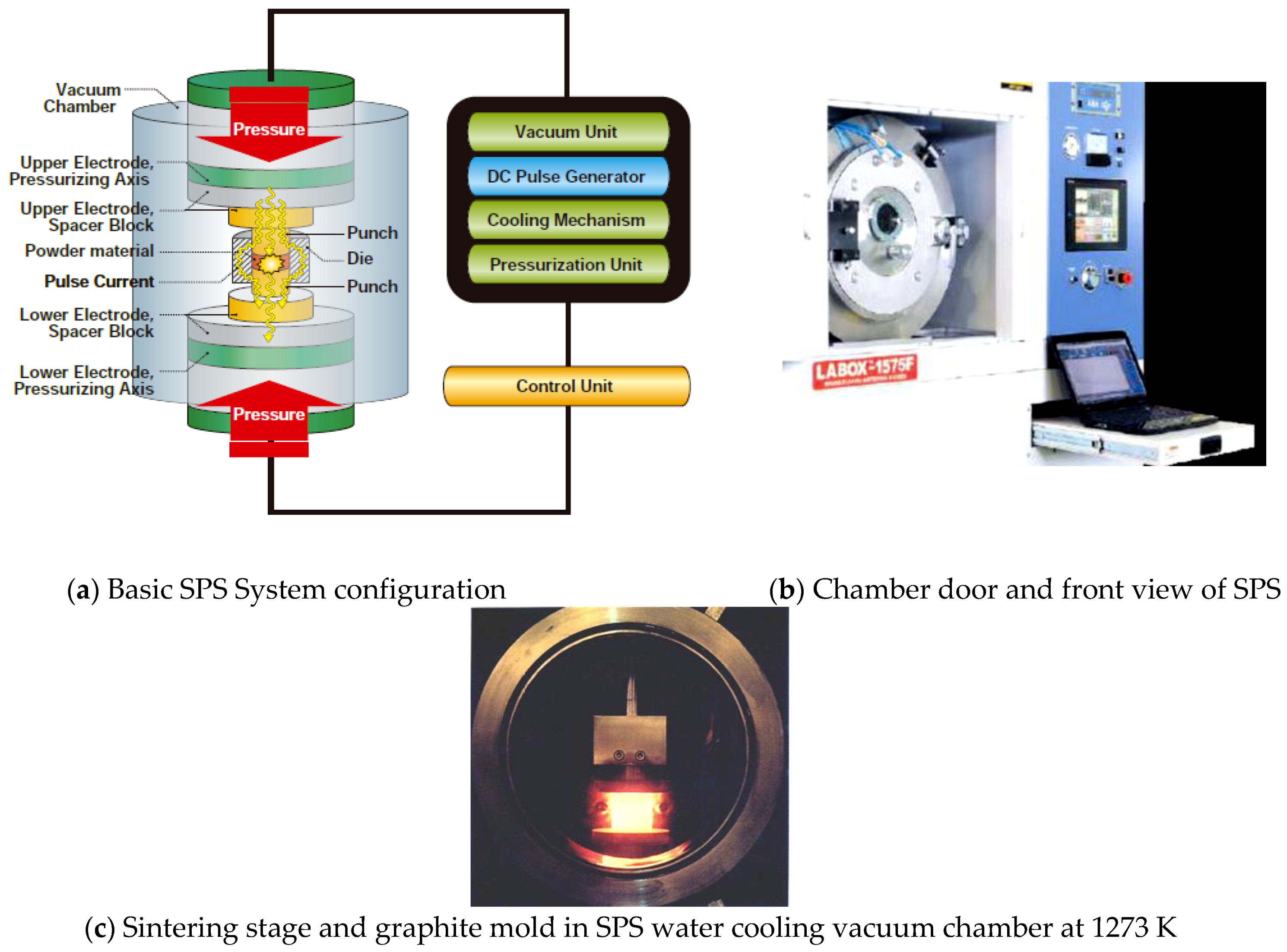
3.2. Basic Configuration of SPS System

Figure 7a shows a schematic diagram of the basic configuration of a typical SPS system. The system consists of a SPS sintering press machine with a vertical single-axis pressurization mechanism, specially designed punch electrodes incorporating a water cooler, a water-cooled vacuum chamber, a vacuum/air/argon-gas atmosphere control mechanism, a special DC-pulsed power generator, a cooling-water control unit, Z-axis position measuring and control unit, temperature measuring and control units, applied pressure display unit, data analyzing unit, and various safety interlock devices. Figure 7b,c photos are a front view of the water-cooled vacuum chamber and inside of the chamber during SPS sintering temperature at 1273 K.

3.3. Basic Mechanism of SPS Process

The SPS process is dynamic non-equilibrium processing whose phenomenon varies from early-stage, mid-stage to late-stage of sintering mechanism, along with reacted material characteristics. Although long years of research work concerning SPS mechanism, by many material researchers, the SPS effect, in other words, the effect of pulsed high current on the generation of spark plasma, peculiar properties in consolidated materials remains unclear [10,21,22,23,24,25,26,27,28,29,30]. There are two major theories on SPS mechanism in discussion. One is with effect of spark and plasma at initial stage, the other is no appearance of spark and plasma during entire SPS process. And, in both theories, it should be noted that metals and ceramics materials show different phenomena. However, based on the theory of with spark example, following is one of the most basic proposed ideas as a mechanism of SPS processing. The ON-OFF DC pulse energizing method generates; (1) spark plasma, (2) spark impact pressure, (3) Joule heating, and (4) an electrical field diffusion effect. In the SPS process, the powder particle surfaces are more easily purified and activated than in conventional electrical sintering processes, and material transfers at both the micro and macro levels are promoted, so a high-quality sintered compact is obtained at a lower temperature and in a shorter time than with conventional processes. Figure 8 illustrates a typical ON-OFF DC current path and how pulse current flows through powder particles inside the SPS sintering using conductive powder material, die, and punch assembly made of graphite material. Conventional electrical hot press processes use DC or commercial AC power, and the main factors promoting sintering in these processes are the Joule heat generated by the power supply (I2R) or high-frequency induction heating elements and the plastic flow of materials caused by the hydraulically or mechanically driving pressure. The SPS process is an electrical sintering technique that applies an ON-OFF DC pulse voltage and high current from a special pulse generator to a powder of particles, and in addition to the factors prompting sintering described above, also effectively discharges between particles of powder to powder and/or graphite die wall surface occurring at the initial stage of the pulse energizing for sintering. When sparking occurred, even one or two sparks, a high-temperature field with sputtering phenomenon generated by spark plasma and spark impact pressure occurs. They work to eliminate adsorptive gases and oxide films and impurities existing on the surface of the powder particles. The action of the electro-magnetic field enhances high-speed diffusion due to the electro-migration effects of ions. The application of the pulse voltage induces various phenomena as shown in Figure 9 in terms of the effects of the ON-OFF DC pulse energizing method. In the case without sparking due to non-conductive material used or the pulse energizing conditions, it is considered that there is still the effect of ON-OFF DC pulse current energizing which provides enhancement of sinterability and densification rate on the material. The large pulsed energy generates an electro-magnetic field-effect such as an electro-migration and preferential orientation of crystalline [31,32].

3.4. Neck Formation and Densification by SPS

When a spark discharge appears in a gap or at the contact point between the particles of a material at an early stage of sintering, a local high temperature-state (discharge column) of several thousands to ten thousands of degrees centigrade is generated momentarily. This causes evaporation and melting on the surface of powder particles in the SPS process, and “necks” are formed around the area of the contact point between particles. Figure 10 shows a basic mechanism of neck formation by spark plasma sintering. Figure 11 is an SEM micrograph showing the result of SPS experiments performed at normal atmospheric pressure (no-load) and 29 MPa applied in a vacuum, with a sintering die and punches made of graphite and a spherical bronze alloy powder (Cu90/Sn10 wt%, particle size 45 μm under). Figure 11a shows the behavior in the initial stage of neck formation due to sparks in the plasma. The heat is transferred immediately from the center of the spark discharge column to the sphere surface and diffused so that the intergranular bonding portion is quickly cooled. As seen in Figure 11b, which shows several necks, the pulse energizing method causes spark discharge one after another between particles. Even with a single particle, the number of portions where necks are formed between adjacent particles increases as the discharges and/or Joule heating is repeated. The Figure 11c shows the condition of an SPS sintered grain boundary which is plastic-deformed after the sintering has progressed further. This state is the result of processing conditions in which the applied pressure was 29 MPa, the SPS sintering temperature was 773 K (measured in the wall of graphite mold), the holding time was 120 s, the SPS current 850 A, and the voltage was 3.9 V. Figure 12a–c and Figure 13 are locally indicating ultra-high temperature field existence between particles as collateral evidence examples of SPS effects on metallic and ceramic materials. It is suggested that the rippled surfaces observed in Figure 12a were caused by the high-temperature state resulting from thermal and sputtering effects of spark plasma and impact pressure by SPS on atomized cast iron at 973 K. Figure 12b shows sintering by pressureless normal sintering at the same temperature affecting only thermal effect. However, as shown in Figure 12c and Figure 13, the local high-temperature state can be observed as a bridging, evaporation, solidification, and/or recrystallization phenomena at SPS sintering temperatures of Fe/973 K, Ni/673 K, Al2O3/1173 K, SiC/1973 K, respectively. These temperatures are 1/2–1/3 lower temperatures than each material’s melting point temperature. Thus, the existence of a local, high-temperature field is suggested [33,34,35,36,37]. It is noticeable that a design of sintering die and punch assembly made of graphite is an extremely important subject to Joule heating according to the sintering progress, interaction of powder material, system resistivity, and the function as direct heating elements in order to assume the role of maintaining the homogeneity of sintering temperature [36,37,38,39].

3.5. DC Pulse Generator for SPS System

Presently, there are two basic types of DC pulse generators for SPS apparatus which are the thyristor-type and invertor-type power supply. The waveform, max/min, ON-time/OFF-time pulse width, peak current, frequency, duty factor settings, control system, energy consumption are different, however, each system has different advantages individually. Therefore, the pulse generator should be chosen to meet the estimated purpose and usage of SPS processing. The majority of SPS systems working in universities, national institutes, and private companies are employed the thyristor-type pulse generator due to its rich reference database on SPS and higher reliability of power supply hardware. The invertor-type with pulse width modulation (PWM) control provides a low power consumption and compact space-saving advantages so that it can be used as an economical low-cost method of production. Dong et al. investigated the effect of a pulsed current waveform on sample temperature and sintering behavior on alumina [40]. However, the detailed development of pulse generators is still in progress. Both thyristor and invertor-types, ON-OFF pulse widths, duty factors, and frequencies are designed to be selectable. Figure 14 and Figure 15 show examples of typical ON-OFF pulse waveforms and different pulse widths and ratios. In thyristor-type generator, pulse ratio of 12:2 is a standard pulse usually.

3.6. Vacuum Exhausting System

SPS processing generally uses a vacuum sintering condition. The system allows operation with an inert gas such as argon gas or nitrogen gas and atmospheric air conditions. By using a rotary vacuum pump with or without a mechanical booster pump, from 1 × 10⁵ Pa (air pressure) to 5–6 Pa within 15 min will normally be applied. Depending on the sintering purpose and usage, SPS vacuum exhausting system can also employ a diffusion pump for a 5–10 × 10−3 Pa high vacuum or a dry pump against a sticky gas.

3.7. SPS Sintering Temperature Measurement Difference

As shown in Figure 8 example, in the SPS process, the sintering temperature is generally measured inside of the graphite die wall by thermo-couple or surface by pyrometer, not in the powder directly. Thus, temperature differences exist between the measured value and an actual filled powder temperature. Figure 16 is an experimental example of nickel powder material indicating 110–120 K difference at 300 s. The heating rate was 2.4 K/s and the open circle in the graph shows sliding surfaces of the graphite punch and die. In accordance with various experiments, it was found that the measured sintering temperatures in both metals and ceramics by SPS were about 50–250 K lower than inside of filled powder material. As with non-equilibrium rapid processing, therefore, SPS sintering temperature in SPS data means this measured temperature [34,36].

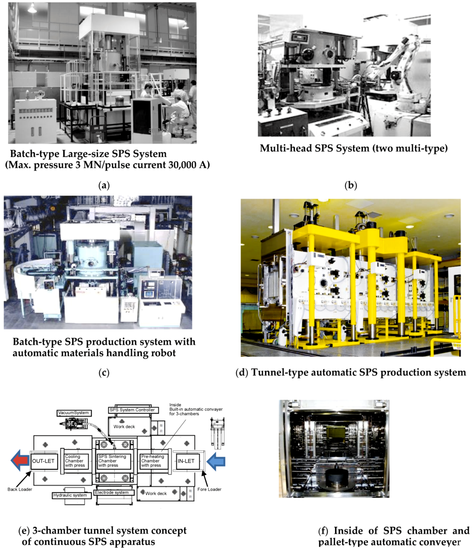
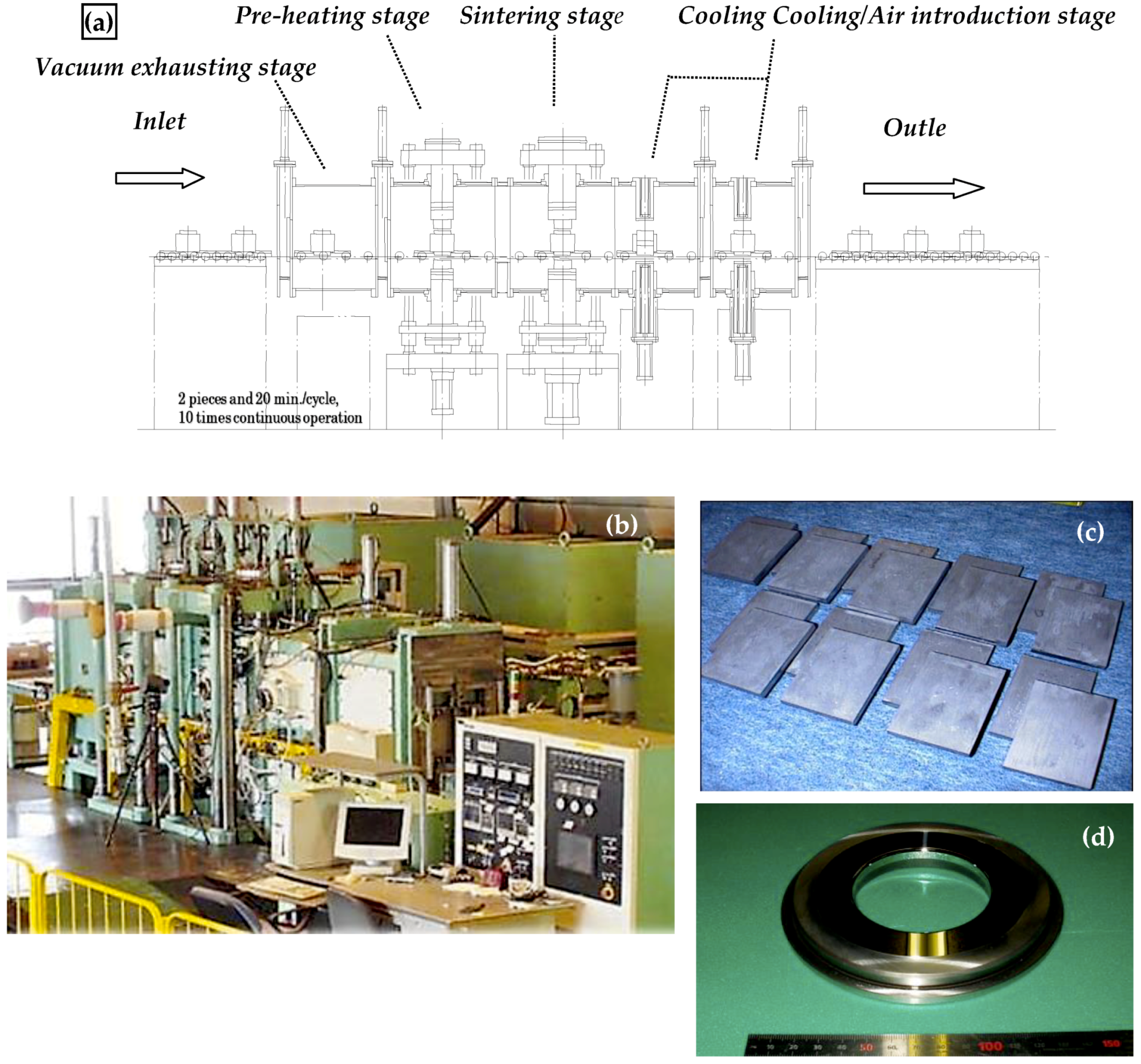
3.8. SPS Production Systems

The development of production type SPS apparatus involves various considerations regarding production strategies which are cycle time, cost and development of optimum systems, and technologies to support scale expansion, automation, mass-production, numerical control (NC) systems, development of process technologies for high functionality, reproducibility, uniformity and structure control, and development of 3D near-net-shape forming techniques so on. Besides, pre and post-process for manufacturing must be considered. As shown in Figure 17, in order to verify SPS productivity, the five basic styles of production-type SPS machine systems have been developed: (1) multi-head SPS systems, (2) batch-type SPS systems, (3) continuous tunnel-type SPS systems, (4) rotary-type SPS systems, and (5) shuttle- type SPS systems. In addition to those, the scaling-up process, automatic handling, powder stacking equipment for materials, and processing optimizers were also developed [12,41,42,43,44,45]. Continuous type of 6 MN SPS press machine incorporated a pallet-type automatic conveyor system manufactured by Sinter land Inc. (Nagaoka, Niigata, Japan) and a single head type of 8 MN SPS with a 150,000 A power supply manufactured by Thermal Technology LLC (Santa Rosa, California, USA) are largest SPS apparatus in the world at present.

4. Typical Example of SPS Phenomena on Ceramics Materials

In past research on SPS, nanophase sintering [46], preferential orientation on TiO2 anatase [32], and single crystal fabrication, etc., [23,47] are typical unique SPS effects. The following are basic SPS effects examples.

4.1. SiC with Al2O3/Yb2O3 Consolidated by SPS and Its Mechanical Properties

Rapid sintering is one of the remarkable futures of SPS. In order to clarify the advantages and mechanism of the SPS method, it was examined on a monolithic ceramic material containing additives. As starting powder materials, 0.28 μm β-SiC with 5 mass%Al2O3/3 mass%Yb2O3 powder was used. Densification behavior and mechanical properties of SPS-consolidated SiC were compared with those of hot-pressed SiC. Figure 18 shows that nearly full densification was attained at about 2023 K for SPS-consolidated SiC and about 2173 K for hot-pressed SiC. In Figure 19, Figure 20 and Figure 21, the optimal bending strength, Vickers hardness, and fracture toughness (not shown) of SPS-consolidated SiC were 720 MPa, 25 GPa, and 4.0 MPa·m1/2, respectively, and these values were higher than those (640 MPa, 23.5 GPa and 3.5 MPa·m1/2) of hot-pressed SiC, respectively, indicating that SPS consolidation can improve the bending strength without degradation of fracture toughness. Pressurization shows a positive effect on the densification enhancement as shown in Figure 21. From XRD and SEM (Figure 22 and Figure 23) and Raman scattering analysis (not shown), it is suggested that a 3C-type disordered structure is preserved in the SPS-consolidated SiC and the improvement of the bending strength without degradation of fracture toughness is attained by the preservation of the 3C-type disordered structure as SPS effect, even enhancement of grain growth of SPSed SiC was larger [48]. When different additives of Al2O3/Y2O3 were used, the SPSed SiC compact had shown a similar tendency as the SPS effect [49].

4.2. Consolidation of Nano-Al2O3, Phase Transformation, and Grain Growth

It is known that the SPS future is to provide microstructure-controlled sintering. The structural tailoring effect in SPS processing was verified in the consolidation of alumina. The capability of SPS processing for the generation of dense nanostructures was investigated by consolidating γ-alumina nano-powder and γ-alumina powders. Up to the present time, SPS consolidation of γ-alumina has been performed for various purposes such as the attainment of high bending strength [50] and the estimation of microstructure inhomogeneity [51], and the relation between process factors and densification behavior [24]. Further, generation of nano-structure due to suppression of grain growth has been indicated in γ-alumina SPS-consolidated at very rapid heating conditions [52,53]. Here, it is shown that the formation of nano-structured dense alumina is possible in conventional SPS conditions by using nano γ-alumina powder. In this study, firstly, the γ-Al2O3 powder particle size of 37 nm, γ-alumina of 0.2 and 0.5 μm were consolidated by SPS method at a heating rate of 160–197 K/min under the pressure conditions of 49 MPa or 690 MPa. Relative density and powder grain size against the consolidating temperature are shown in Table 3. In Figure 24, the γ-alumina was fully densified at 1673 K under the pressurizing condition of 49 MPa, while γ-alumina full densification was attained at 1773 K. When the pressure increased to 690 MPa (Figure 25), nano-structured 98% dense alumina with a grain size less than 500 nm was obtained at the conditions of 1173 K. Figure 26 shows the phase transformation of γ-Al2O3 prepared at 1173–1473 K under 49 MPa.
As shown in Figure 25 and Figure 27, it was found that density decreased at 973 K due to phase change to δ and θ-phase. Under the high pressure of 690 MPa, the sintering underwent nearly full densification of γ-alumina at 600 K, a lower temperature [54]. Secondarily, when α-alumina powder with a grain size of 100 nm used, a consolidation by SPS method performed at the heating rate of 123 K/min under the pressurizing conditions of 30 MPa or 100 MPa shown in Figure 28. Nano-structured dense alumina with a grain size less than 300 nm, 99.18%TD was synthesized under the conditions of 1423 K and 100 MPa. At the same, 1423 K with 30 MPa, the sintered one reached 86.9% TD. To obtain a 98.3% TD-dense alumina compact with 30 MPa, a higher temperature of 1473 K was required. In Figure 28, fractured surfaces of FE-SEM, it is indicated that the difference in the applied pressure at the consolidation temperature of 1423 K drastically changes the microstructure in the SPS-consolidated α-Al2O3. That is, full densification and nano-structure can be attained by SPS consolidation when the preferable pressurizing condition is selected without selecting such a high heating rate. The heating rate is more important for the synthesis of a dense nano-structure and highly transparent alumina, though applied pressure is also correlated with the generation of the structural tailoring. The findings suggest that it is important to select an optimum combination between SPS parameters and heating rate that is delicately effective for generating new micro/nano-structures in the SPS-consolidated ceramics [55]. High-temperature short-period SPS sintering is expected to provide almost all ceramic materials with new characteristics and sintered effects that are different from those obtained by the HP and HIP processes. On Al2O3, Nygren, et al. investigated and reported detailed SPS effects including grain growth and SPS sintering conditions [24].

4.3. Examples of Nano Structural Ceramic Materials

BaTiO3 ceramics are a well-known ferroelectric material with a high permittivity at room temperature and providing various industrial applications, for instance, the thermistor, multilayer capacitor, and optic devices, etc.
Takeuchi et al. prepared dense BaTiO3 ceramics consisting of sub-micrometer grains using the SPS process [56]. As starting powder, a material of 100–500 nm size was used, under 39 MPa pressure, 1000–1200 °C of SPS sintering temperature with 5 min holding time, more than 95% of theoretical density was obtained. The average grain size of the SPSed pellet was less than 800 nm. Compared with the conventional hot press process on the same starting powder, due to minimized grain growth and finer than HPed BaTiO3, SPSed BaTiO3 achieved a much better permittivity of 7000 at 1 kHz at room temperature (Figure 29).
Anselmi-Tamburini, Garay and, Munir prepared and reported nano oxide ceramics of dense ZrO2 and CeO2 with grain sizes approaching 10 nm, applying a high-pressure method up to 1 GPa using a special SPS sintering die and punches assembly as shown in Figure 30. A sample 5 mm in diameter and 1–3 mm thick, starting powder grain size 7–8 nm, under a vacuum condition, up to 1 GPa and holding pressure 530–610 MPa at 625–850 °C, attained over 98% relative density with minimized grain growth of 11–18 nm grain size sintered compacts [57].
Ohyanagi, et al. also researched pure (no additives) nano SiC consolidation using MA powder. A starting powder size of 30 nm was used, applying 40 MPa, SPS sintering temperature 1700 °C, and heating rate 180 °C/min, holding time from 0 to 30 min, specimen size of 19 mm diameter, 5 mm thick, R.D 98% of dense SiC with an approximate grain size of 100 nm was obtained [58]. Comparing to commercially available CVD 30 nm SiC powder material, this result was extremely lower sintering temperature. They found a disorder-order transformation effect on MA-SiC powder material. Presently, it is possible to prepare pure SiC compact R.D 99.4%with minimized grain growth and obtained Hv2380 hardness (refer to Figure 6).
A nano-microstructure controlled sintering method is a major key advantage of the SPS sintering technique. Many nanophase ceramics, ceramics composite material research work has demonstrated this during past ten to fifteen years. Further, performing easy solid-phase sintering effects is one of the SPS features that allow pure nano-WC powder to be sintered at 99–100% relative density and has successfully been commercializing in optical equipment industry for the various glass lens mold and die applications to date.

4.4. Examples of Synthesized Functionally Graded Materials (FGMs) by SPS

SPS has been used successfully to synthesize a wide range of bulk FGM materials with three to eight (or up to 19) intermediate mixed layers utilizing unique a SPS temperature gradient sintering method. FGMs are widely recognized as “dream-like advanced new materials”. For instance, multi-layered ceramic-metal system FGMs represent one material having different characteristics. This concept originated in Japan in 1984. Figure 31 shows typical examples of bulk FGMs compacts synthesized by SPS. From the left, a ZrO2(3Y)/SUS stainless steel compact with 6 interlayers, a ZrO2(3Y)/nickel compact with 7 interlayers, a copper/stainless steel (SUS) compact with 5 interlayers, an aluminum/polyimide compact with 3 interlayers, and on the right, an Al2O3/titanium compact with 3 interlayers. Full density and no micro-cracks were detected in the sintered compacts obtained by the SPS process. All were sintered in ten to twenty-five minutes heating up and keeping time, and a diameter of 20–50 mm after the start of the process. Various combinations of FGMs systems of ZrO2/SUS (stainless steel), ZrO2/TiAl, ZrO2/Ni, Al2O3/SUS, Al2O3/Ti, Al2O3/Ti-6Al-4V, HAP/Ti, TiN/HAP, WC/SUS, WC/Co, WC/Ni, Cu/SUS, SiO2glass/SUS, Al/polyimide resin, Cu/phenol resin, and Cu/polyimide resin materials, etc., were prepared [59,60,61,62,63,64,65]. Figure 32 shows a schematic illustration of SPS temperature gradient die assembly and an example of multi-layered ZrO2(3Y)/SUS stainless steel FGMs compact which contains a 3 mol% yttrium partially stabilized zirconia (PSZ) powder, SUS410L stainless steel (SUS) powder, and mixed powders of the two as intermediate layers with different volume fractions. The FGM powder was stacked in a graphite temperature-gradient die of 20 mm internal diameter. The SUS powder has an average particle size of 9 μm while the PSZ powder consists of granulated particles with an average particle size of 50 μm (its crystalline size is 350 Å). Sintering pressures used were 20 to 40 MPa, SPS temperatures of 1243–1293 K, with a temperature rise rate of 50 K/min. measured near the SUS layer [60].

4.5. 3D Near-Net Shape/Net Shape Forming

Three-dimensional (3D) near-net shape and/or net shape forming is another SPS advantage as an industrial manufacturing process for production cost reduction. Because of a cavity or through-hole die used SPS method, depending on appropriate die material selection and die design, it is possible to provide 3D near-net/net shape sintering. As shown in Figure 33, a healthy dense ceramics-metal system of ZrO2/Ti/Ti-6Al-4V FGMs can be developed by a combination of 3D and FGMs techniques. This SPSed compact 80 mm in diameter has 5 layers consisting of 100% of ZrO2 top layer, ZrO2-Ti, Ti, Ti-Al alloy 3 interlayers, and 100% of Al alloy layer at the bottom. The obtained relative density of ZrO2 100% top layer was 99–100% without any residual pores, cracks, and delaminations.

5. Ceramics Applications by SPS

5.1. Nanoparticle of Pure WC (Tungsten Carbide) Aspheric Glass Lens Mold

The necessity of in-vehicle camera systems, camera devices for monitoring roads, and surveillance cameras are sharply increasing due to upcoming demands under today’s social safety circumstances. The establishment of a cost-effective fabrication method of a high-performance aspheric glass lens for digital cameras is an essential key technology to comply with these recent industrial requirements. Figure 34 is an example of an SPSed component in actual commercial use in the optic industry, which is an aspheric glass lens mold made of a binder-less pure-tungsten carbide (WC single-phase, Hv2600) material without any additives except inevitable impurities. As the starting powder materials, an average particle size of less than 200 nm or 80 nm are used. They were homogeneously consolidated in nano-structured fine grain size. Post-processing using an ultra-precision grinding machine, the superfinishing of mirror surface roughness of Ra 2–6 nm can be obtained to be used in digital camera lens application. The aspheric glass lens mold is consisting of three pieces that of upper punch, lower punch and sleeve die part. Advantages of SPSed pure WC material are no additives solid-phase sintering, finer grain size, and higher oxidation resistance compared to conventionally produced other binder-less WC materials indicated in Figure 34. By running the 10 h oxidization test in an atmospheric furnace at 973 K, it was demonstrated 30–60% better oxidization rate per volume (g/cm2).

5.2. 3-Dimensional Complex Net- Shape Forming of Al2O3 Blasting Nozzle

Figure 35 shows an example of an Al2O3 ceramic nozzle for a sand-blasting machine. The actual lifetime was investigated under the same blast operating conditions. The SPSed Al2O3 nozzle achieved a ten times longer life span than the conventionally sintered one made by an atmospheric pressureless sintering furnace. The photos show sintered nozzle shapes made by SPS without any post-processing such as mechanical grinding and polishing, producing a Vickers hardness of Hv2100–2200, and the 3-D “net-shape” accuracy with Ra 0.64 μm surface roughness. To eliminate the usual mechanical grinding post-process for the nozzle parts finishing, the new production method of nozzle net-shape forming has been developed by SPS.

5.3. Near-Net Shape Formed Si3N4/Al2O3 Composite Compacts for Homogenizer Component

Figure 36 is an example of a fine ceramic sintered compact for homogenizer’s wear-resistant parts. Studying its thermal expansion ratio for the usage, the composition of mixed starting powder was 50% Si3N4 and 50% of Al2O3. SPS rapid sintering process could achieve shorter production time and minimized grain growth resulting in a harder sintered compact of over Hv20 GPa hardness with a high relative density of 99% to 100%. Pressurized sintering allows for the direct sintering from powders to near-net-shape dimensions of ring or cylindrical shape and eliminating the green body compaction process of normal pressureless sintering. The sintering conditions were SPS temperature 1673 to 1873 K with heating–up and holding time of approx. 15–20 min, and applied pressure 30 to 50 MPa. The tolerances of as-sintered parts ensure within 0.2 to 0.3 mm accuracy so that it is easy to obtain a final finishing accuracy by conventional mechanical grinding as its post process.

5.4. Sputtering Target Material and Fabrication of Large-Sized Ceramics and Metals Compact

With the SPS process, highly dense sintered products can be fabricated at a much lower temperature and higher purities, finer microstructures with shorter heating up and holding times compared with conventional hot pressing and HIPing. Thus, sputtering target material fields are one of the very effective suitable industrial applications for SPS. Several companies have already been manufacturing their target material products using several sets of large SPS machine systems simultaneously in their production plant. Figure 37 shows typical examples of large-sized SPSed ceramics materials. Large-sized oxide ceramics (Al2O3, ZrO2, SiO2, etc.), carbide (WC, SiC, B4C), nitride (Si3N4), and boride (TiB2) ceramic materials were well fabricated homogenously with finer grain size and almost full density. As seen in Figure 37, dense Φ300 mm Al2O3 is available, however, due to limited present SPS machine heating capability and operational know-how, in case of high-temperature materials of carbide and nitride ceramics, for full densification, up to 150–200 mm diameter can be manufactured that of smaller size than oxide ceramics. As a practical industrial application, further improvement will be required. The SPSed target materials are investigated by SEM observation that nearly no residual micropores and no cracks were detected in the large-size disk-shaped sintered compacts. Ruthenium sputtering target material in diameters of Φ350 mm also produced by production-type large-size SPS apparatus. The productivity is approximately 7 to 8 times higher than conventional sintering of HP and HIP processes. Because the obtained finer grain size of SPSed sputtering target materials, it can provide superior sputtering performances such as no splashing phenomenon in the coating process. The samples shown in Figure 38, were typical examples of metallic sputtering target materials.

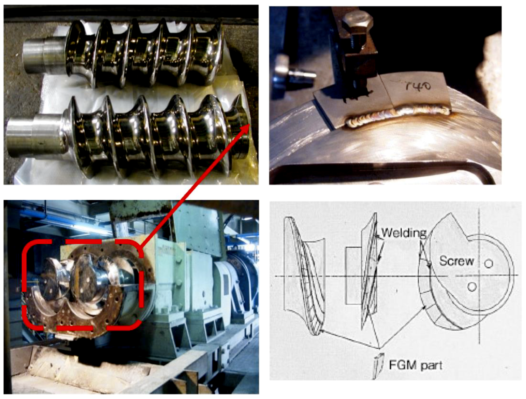
5.5. Development of Al2O3/Ti System FGMs and ZrO2/Ti/Ti-6Al-4V Alloy FGMs Horn Tip Tool for Ultra-Sonic Homogenizer

The 100% ceramic layer was composed of an α-Al2O3 powder with an average particle size of 0.22 μm purity 99.99% and the ceramic-metal interlayers were composed of α-Al2O3 and pure titanium powder with an average particle size 10 μm 99% purity, and 100% metal layer was used Ti-6Al-4V powder with an average particle size 100 μm as substrate material. These powders were combined into the mixtures with wet mixing by a planetary ball milling. The graded layer having 10 layers of Al2O3 100%, Al2O3/Ti composition of 95/5, 95/10, 85/15, 80/20, 70/30, 60/40, 50/50, 30/70 vol%, and Ti-6Al-4V 100% were prepared. Each of the FGM interlayers was of 0.5 mm thickness after sintering. DC pulse voltages from 12 to 2 volts were applied. And it was held at 1223 K-1573 K for holding time 0–10 min, under the sintering pressure of 20–70 MPa in vacuum condition, then the pulse energizing was stopped and the specimen was cooled. To evaluate the microstructure of the sintered FGMs, a cross-section of a mirror-polished specimen was observed using optical microscopy and EDS/EPMA. As shown in Figure 39, observing the healthy dense disk-shaped 8-interlayers FGM sintered compact with a total thickness of 10.5 mm, no micro-cracks, no pores, and no de-laminations were detected. The Vickers hardness of the Al2O3 100% layer was 19.5 GPa.
Industrial applications of Al2O3-Ti-Ti alloy system FGMs and hydroxyapatite (HAP)-Ti system FGMs are mainly investigated for biocompatible materials such as artificial bones, hip bone joints, and dental implants [61,66]. As a practical industrial application based on the optimized sintering conditions of oxide ceramics of Al2O3/Ti-Ti alloy FGMs, 5 layered ZrO2/Ti/Ti-6Al-4V alloy system FGMs was developed and presently commercialized for horn tip parts of ultra-sonic homogenizer equipment shown in Figure 40.
The FGMs profile was studied and finally reached at 5 layers incorporating ZrO2/Ti mixed powder of three interlayers. Figure 41 shows ZrO2/Ti alloy system FGMs profile and optimized sintering conditions on topcoat behavior with SEM image. SPS sintering temperature of 1573 K at sintering pressure 30 MPa attained the lowest 17.0 mg wear amounts after the homogenizing test.
Various types of FGMs horn tip tools for ultrasonic homogenizer were manufactured as shown in Figure 42. Due to a dense ceramic material with a high hardness on the surface, it clearly improved the cavitation corrosion resistance in homogenizing. The lifetime of the horn tip made of ZrO2/Ti/Ti-6Al-4V alloy FGMs achieved more than 8–10 times longer life span than conventional one without cracking, peeling off, and breaking down. The conventional horn tip tool made of titanium is chemically stable and mechanically easy to perform the desired shape, however, its low wear resistance generates needless contamination and a short lifetime. A Brazed ZrO2 plate on the Ti body horn tip also indicates weakness at the brazed layer. The monolithic ceramic horn tip has good hardness, however, brittle and breakable and short lifetime against a high oscillating frequency of 19.5 kHz. On the other hand, the ceramic-metal system FGMs horn tip provided a good hardness of Hv1364, higher toughness, and long life compared to a conventional Ti horn tip. It is expected that fewer contamination effects will present a highly reliable production process for the electronics industry and available large-sized horn tips encourage higher out-put power oscillation with much better productivity [67].

5.6. WC Matrix Diamond Dicing Blade for Cutting Tool Industry

As shown in Figure 43, a typical example of the SPSed mass products has already been realized in the practical use in cutting tools and wear-resistant materials industry. The 2-shifts or 3-shifts per day and continuous night working time in the production factory, simultaneous multi fabrication of 15–20 plates per batch are being carried out. The Co metal bonded WC dicing blade (cutting tool) of 100/150 mm diameter and 0.35/0.4 mm thickness were produced providing the flatness within ±20 μm with minimal residual stresses. Sintered WC/Co plate of relative density 99–100% and Young’s moduli of 500–580 GPa were attained under SPS temperatures of 1473–1523 K. As sintered plates obtained such flatness by SPS, the grinding process was eliminated and the production cost was greatly reduced. This example is an effective SPS near-net/net shape forming process. A Cu-based very thin dicing blade of less than 0.3 mm width is also manufactured by SPS. Several companies have been using multiple units of SPS apparatus for their actual production.

5.7. Fine WC/Co Hard Alloy FGMs for Die & Mold and Wear Resistant Materials Industries

As a typical high wear-resistant material, WC/Co or WC/Ni system cemented carbides are now widely used in various press-stamping dies and cutting tools for industrial applications. Although fabrication of WC/Co system hard alloys usually takes many hours by conventional sintering processes, with the development of a new automated SPS production system, it is now possible to sinter such materials in a significantly shorter period taking advantage of the characteristics inherent in SPS rapid sintering technology. Table 4 is the typical mechanical properties of SPSed fine WC/Co system hard alloy and binder-less nano grain WC products. Figure 44 shows the production machine system configuration and outside view of the fully automated 5-stage chamber type SPS production system (continuous furnace) incorporating pallet-type automatic conveyor. Utilizing this full tunnel-type automated SPS system and optimized SPS conditions, square-shaped large-size WC/Co cemented carbide hard-alloy with dimensions of 70 mm (width) × 100 mm (length) × 5–20 mm (thickness) were homogeneously fabricated in a shorter sintering time and with a finer grain size than with conventional sintering methods while maintaining high quality and repeatability every 10 min or less per piece as shown in Figure 44 (right photo of (c)). The fine-WC/Co hard alloys (product code name TC05/10/20), obtained by SPS, provide higher hardness, transverse rupture strength, and fracture toughness than those obtained by conventional sintering methods. The usage of SPSed WC/Co super-hard alloy materials are mainly wear-resistant drawing die, press stamping die, IC lead frame die, cutting tools, and various kinds of wear-resistant industrial components.

5.8. Examples of WC/Co and WC/Co/Ni FGMs for Industrial Applications

Near-net shape forming and scaling-up process on square-shaped FGMs were studied. The cobalt content compositionally graded square-shaped large-size WC/Co FGMs with dimensions of 100 mm (width) × 100 mm (length) × 40–60 mm (thickness) was successfully synthesized within an hour shown in Figure 45. The sintered bulk FGMs was machined by a numerically controlled wire-cut electrical discharge machine (EDM) to cut off from the large bulk material to the small pieces of FGMs. As indicated in Figure 46, the small piece of WC/Co FGMs is ground to form the specified profiles with necessary accuracies and tolerances as press stamping dies and punches by grinding machine. The SPSed fine WC/Co FGMs hard alloy had high hardness on the topcoat layer and higher strength and fracture toughness on the bottom side than the monolithic WC/Co hard alloy material. When assembled into press stamping progressive die set, it achieved an approximately 3.5 to 10 times longer lifetime compared with conventional commercial WC/Co cemented carbide. The 3-layered weldable WC/Ni FGMs screw for the extruding machine was also developed as shown in Figure 47 and Figure 48. Square-shaped WC/Ni FGM tiles were manufactured in four simultaneous pieces by a 4-multiple sintering method. The assembled screw lifetime was over three times longer (3000 h against 800 h) than a conventional screw. In Japan, this FGMs screw has been working well for many years at the Hokkaido Electric Power company [68].

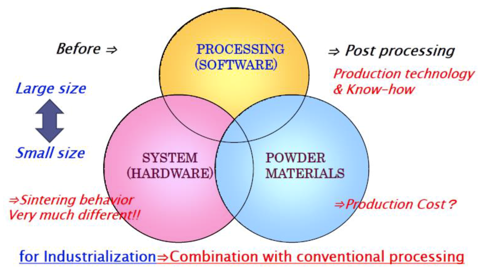
5.9. Other Industrial Applications by SPS and Recent Demands from Industries

Using the SPS process, research work on nanostructured materials and composite materials is very attractive and active to date. Many investigations on ceramics materials have been conducted [69,70,71,72,73]. Considering the effective SPS industrialization, as introduced in Figure 33, Figure 35, Figure 36, and Figure 43, it is expected that the SPS 3D near-net/net shape forming method will be applied for parts production from R&D prototype level to practical mass production use in the near future [74]. Besides, in order to accomplish successful industrialization, the appropriate combination of post-processing techniques is important in the actual product manufacturing process. Conventional mechanical cutting, grinding, electrical discharge machining (EDM), laser machining, and surface treatment techniques are essential production elements. Due to the rapid sintering process, SPS sintering behavior and conditions usually vary between 20–30 mm diameter of small size and 100–300 mm diameter of large size. To comply with the SPS size effect and shape effect, it requires enlargement management know-how to attain dense and homogeneous SPS sintered materials. Although SPS research and development on other categories of materials both of ceramics and metals were not discussed in this paper, such as transparent ceramics [75,76,77,78], MMC/FRC/FRM [79,80,81,82], CNT/CNF various composite materials [83,84,85,86,87,88,89,90,91,92,93], thermo-electric semiconductors of SiGe, Bi2Te3, FeSi2, CoSb3, MnSi2, Mg2Si, MgFe2O4 systems for clean energy generation [94,95,96,97,98], nuclear materials [99], Nd-Fe-B, Sm2Co17 and ferrite for magnetic materials [100,101], MgB2 superconducting materials [102], PbTiO3 dielectric materials [103], lithium battery [104], shape memory alloys, solid cell materials, glassy metals, and optically functional materials, nevertheless, they are promising candidates for industrial SPS applications. Ceramic-ceramic solid-phase SPS bonding processing is also attractive for industries. In order to pursue the optimum manufacturing method by SPS technology, it should be considered the trinity of hardware strategies, software, and powder material technologies as combined R&D factors mentioned in Figure 49. New approaches have been demonstrated to clarify the characteristics of pulsed current sintering of SPS and flash sintering method [105,106,107,108,109,110,111]. Recent demands on SPS technologies from industries are briefly suggested in Figure 50.

6. Conclusions

In this paper, SPS history, fundamentals, and the wider availability of SPS in ceramics materials and its related industrial applications were introduced. Especially, typical advantages of SPS processing were indicated in the synthesis of nanocrystalline materials, FGMs, and wear-resistant hard materials. Because of the versatility of SPS, it should be noted that the remarkable rapid growth in the number of presented papers and patents in the last decade resulted from the worldwide spread of the SPS technology in both the scientific community and the industrial sector. SPS features an electrical energy concentration at areas where current flows easily. In terms of the high energy density of dynamical sintering, the study on these characteristics will lead us to the successful advancement and expanded SPS applications for reasonable commercial production. The SPS technology has a high potential to become a major product manufacturing tool in the automotive, electronics, mold and die, tooling, clean energy, and aerospace industries, therefore, is now focusing on both high-value-added, small scale, and mass-production.

Funding

This research received no external funding.

Institutional Review Board Statement

Not applicable.

Informed Consent Statement

Not applicable.

Conflicts of Interest

Authors declare no conflict of interest.

References

  1. Tokita, M. Development of Advanced Spark Plasma Sintering (SPS) Systems and Its Industrial Applications. Ceram. Trans. Am. Ceram. Soc. 2006, 194, 51–60. [Google Scholar]
  2. Munir, Z.A.; Anselmi-Tamburini, U.; Ohyanagi, M. The effect of electric field and pressure on the synthesis and consolidation of materials: A review of the spark plasma sintering method. J. Mater. Sci. 2006, 41, 763–777. [Google Scholar] [CrossRef]
  3. Grasso, S.; Sakka, Y.; Maizza, G. Electric current activated/assisted sintering (ECAS): A review of patents 1906–2008. Sci. Technol. Adv. Mater. 2009, 10, 1–24. [Google Scholar] [CrossRef]
  4. Hungria, T.; Galy, J.; Castro, A. Spark Plasma Sintering as a Useful Technique to the Nanostructuration of Piezo-Ferroelectric Materials. Adv. Eng. Mater. 2009, 11, 615–631. [Google Scholar] [CrossRef]
  5. Inoue, K. Electric Discharge Sintering. U.S. Patent No. 3,241,956, 22 March 1966. Ser.No.247,387 filed 29 October 1963. [Google Scholar]
  6. Inoue, K. Apparatus for Electrically Sintering Discrete Bodies. U.S. Patent No. 3,250,892, 10 May 1966. filed 29 December 1962. [Google Scholar]
  7. Taylor, G.F. Apparatus for Making Hard Metal Compositions. U.S. Patent No.1,896,854, 7 February 1933. [Google Scholar]
  8. Cremer, G.D. Sintering Together Powders Metals such as Bronze, Brass or Aluminum. U.S. Patent No. 2,355,954, 15 August 1944. [Google Scholar]
  9. Tokita, M. Trends in Advanced SPS Spark Plasma Sintering Systems and Technology. J. Soc. Powder Technol. Jpn. 1993, 30, 790–804. [Google Scholar] [CrossRef] [Green Version]
  10. Tokita, M. Mechanism of Spark Plasma Sintering (SPS). In Proceedings of the PM2000 Powder Metallurgy World Congress, Kyoto, Japan, 12–16 November 2001; Part-I. pp. 252–255. [Google Scholar]
  11. Tokita, M. Development of Automatic FGM Manufacturing Systems by the Spark Plasma Sintering (SPS) Method. Ceram. Trans. Am. Ceram. Soc. 2001, 114, 283–290. [Google Scholar]
  12. Tokita, M. Method and System for Automatic Electrical Sintering. U.S. Patent No. 6,383,446 B1, 7 May 2002. [Google Scholar]
  13. Miyasaka, Y.; Tokita, M.; Karasawa, H.; Nishiyama, F. Electric Joining Methods and Apparatus and a Joined Unit of Members. U.S. Patent No. 6,515,250, 4 February 2003. [Google Scholar]
  14. Kawahara, M.; Tokita, M. New Application Fields of Spark Plasma Sintering (SPS) Technology Application examples of SPS for Surface Modification. In Corrosion Engineering; Allerton Press: Tokyo, Japan, 2001; Volume 50, pp. 63–71. [Google Scholar]
  15. Prawara, B.; Yara, H.; Miyagi, Y.; Fukushima, T. Spark plasma sintering as a post-spray treatment for thermally-sprayed coatings. Surf. Coat. Technol. 2003, 162, 234–241. [Google Scholar] [CrossRef]
  16. Khor, K.A.; Chen, X.J.; Chan, S.H.; Yu, L.G. Microstructure-property modifications in plasma sprayed 20 wt.% yttria stabilized zirconia electrolyte by spark plasma sintering (SPS) technique. Mater. Sci. Eng. 2004, A366, 120–126. [Google Scholar] [CrossRef]
  17. Makino, Y. Crystallographic behaviors of nano-powder anatase consolidated by SPS method. Pulse Electr. Curr. Synth. Process. Mater. 2006, 301–312. [Google Scholar] [CrossRef]
  18. Yu, M.; Grasso, S.; Mckinnon, R.; Saunder, T.; Reece, M. Review of flash sintering: Materials, mechanisms, and modelling. Adv. Appl. Ceram. 2016, 116, 24–26. [Google Scholar] [CrossRef] [Green Version]
  19. Olevsky, E.A.; Rolfing, S.M.; Maximenko, A.L. Flash (Ultra-Rapid) Spark-Plasma Sintering of Silicon Carbide. Sci. Rep. 2016, 6. [Google Scholar] [CrossRef] [Green Version]
  20. Du, B.; Gucci, F.; Porwal, H.; Grasso, S.; Mahajanb, A.; Reece, M.J. Flash spark plasma sintering of magnesium silicide stannide with improved thermoelectric properties. J. Mater. Chem. C 2017, 5, 1514–1521. [Google Scholar] [CrossRef] [Green Version]
  21. Matsugi, K.; Hatayama, T.; Yanagisawa, O. Effect of Direct Current Pulse Discharge on Specific Resistivity of Copper and Iron Powder Compacts. J. Jpn. Inst. Met. 1995, 59, 740–745. [Google Scholar] [CrossRef] [Green Version]
  22. Ozaki, K.; Kobayashi, K.; Nishio, T.; Matsumoto, A.; Sugiyama, A. Sintering Phenomena on Initial Stage in Pulsed Current Sintering. J. Jpn. Soc. Powder Powder Metall. 2000, 47, 293–297. [Google Scholar] [CrossRef]
  23. Omori, M. Sintering consolidation, reaction and crystal growth by the spark plasma system (SPS). Mater. Sci. Eng. 2000, A 287, 183–188. [Google Scholar] [CrossRef]
  24. Shen, Z.; Johnsson, M.; Zhao, Z.; Nygren, M. Spark Plasma Sintering of Alumina. J. Am. Ceram. Soc. 2002, 85, 1921–1927. [Google Scholar] [CrossRef]
  25. Schmidt, J.; Niewa, R.; Schmidt, M.; Grin, Y. Spark Plasma Sintering Effect on the Decomposition of MgH2. J. Am. Ceram. Soc. 2005, 88, 1870–1874. [Google Scholar] [CrossRef]
  26. Song, X.; Liu, X.; Zhang, J. Neck Formation and Self-Adjusting Mechanism of Neck Growth of Conducting Powders in Spark Plasma Sintering. J. Am. Ceram. Soc. 2006, 89, 494–500. [Google Scholar] [CrossRef]
  27. Chaim, R. Densification mechanisms in spark plasma sintering of nanocrystalline ceramics. Mater. Sci. Eng. 2007, A443, 25–32. [Google Scholar] [CrossRef]
  28. Misawa, T.; Shikatani, N.; Kawakami, Y.; Enjoji, T.; Ohtsu, Y. Influence of Internal Pulsed Current on the Sintering Behavior of Pulsed Current Sintering Process. Mater. Sci. Forum. 2010, 638, 2109–2114. [Google Scholar] [CrossRef]
  29. Hulbert, D.M.; Anders, A.; Dudina, D.V.; Andersson, J.; Jiang, D.; Unuvar, C.; Anselmi-Tamburini, U.; Lavernia, E.J.; Mukherjee, A.K. The absence of plasma in “spark plasma sintering”. J. Appl. Phys. 2008, 104, 033305. [Google Scholar] [CrossRef] [Green Version]
  30. Zhang, Z.H.; Liu, Z.F.; Lu, J.F.; Shen, X.B.; Wang, F.C.; Wang, Y.D. The sintering mechanism in spark plasma sintering–Proof of the occurrence of spark discharge. Scr. Mater. 2014, 81, 56–59. [Google Scholar] [CrossRef]
  31. Groza, J.R.; Zavaliangos, A. Sintering activation by external electrical field. Mater. Sci. Eng. 2000, A287, 171–177. [Google Scholar] [CrossRef]
  32. Makino, Y.; Mori, T.; Eguchi, H.; Yoshioka, T.; Saito, H.; Kyoh, B.; Miyake, S. Dense nano-structured and preferentially-oriented anatase synthesized by pulsed high current heating. J. Jpn. Soc. Powder Powder Met. 2005, 52, 805–811. [Google Scholar] [CrossRef]
  33. Nanko, M.; Maruyama, T.; Tomino, H. Neck Growth on Initial Stage of Pulse Current Pressure Sintering for Coarse Atomized Powder Made of Cast-Iron. J. Jpn. Inst. Metals. 1999, 63, 917–923. [Google Scholar] [CrossRef] [Green Version]
  34. Kumeta, K.; Nakamura, Y.; Takada, A.; Ishizaki, K. Surface Observation of Pulsed Electric Sintered Alumina Balls. J. Jpn. Cerem. Soc. 1999, 107, 187–189. [Google Scholar] [CrossRef] [Green Version]
  35. Kim, H.T.; Kawahara, M.; Tokita, M. Specimen Temperature and Sinterability of Ni Powder by Spark Plasma Sintering. J. Jpn. Soc. Powder Powder Metall. 2001, 47, 887–891. [Google Scholar] [CrossRef] [Green Version]
  36. Hirai, T.; Tokita, M.; Pan, W.; Chen, L.D.; Omori, M. Porous Silicon Carbide Sintered Compacts and Fabrication Method. JP. Patent No. 4,398,027, 30 October 2009. [Google Scholar]
  37. Zavaliangos, A.; Zhang, J.; Krammer, M.; Groza, J.R. Temperature evolution during field activated sintering. Mater. Sci. Eng. A. 2004, 379, 218–228. [Google Scholar] [CrossRef]
  38. Matsugi, K.; Kuramoto, H.; Hatayama, T.; Yanagisawa, O. Temperature distribution at steady state under constant current discharge in spark sintering process of Ti and Al2O3 powders. J. Mater. Process. Technol. 2004, 146, 274–281. [Google Scholar] [CrossRef]
  39. Tiwari, D.; Basu, B.; Biswas, K. Simulation of thermal and electric field evolution during spark plasma sintering. Ceram. Int. 2009, 35, 699–708. [Google Scholar] [CrossRef]
  40. Dang, K.Q.; Kawahara, M.; Takei, S.; Nanko, M. Effect of Pulsed Current Waveform on Sample Temperature and Sintering Behavior in PECS of Alumina. J. Jpn. Soc. Powder Powder Metall. 2009, 56, 780–789. [Google Scholar] [CrossRef] [Green Version]
  41. Tokita, M. Apparatus for Multiple Head-Type Spark Plasma Sintering. JP. Patent No.3,618,630, 19 November 2004. [Google Scholar]
  42. Tokita, M.; Nakagawa, K. Method and System for Rotary Table-type Pulsed Electric Current Sintering. JP. Patent No. 3,645,811, 2007. [Google Scholar]
  43. Tokita, M.; Nakagawa, K.; Suzuki, S. Method and Apparatus for Shuttle-type Spark Plasma Sintering System. JP. Patent No. 3,822,174, 30 June 2006. [Google Scholar]
  44. Tokita, M.; Suzuki, S.; Nakagawa, K. Nano-Precision Sintering System. U.S. Patent No. 7,547,204, 16 June 2009. [Google Scholar]
  45. Tokita, M. Method and Apparatus for Automatically Loading Powder into a Mold. U.S. Patent No. 6,881,048 B1, 19 April 2005. [Google Scholar]
  46. Nygren, M.; Shen, Z. On the preparation of bio-, nano- and structural ceramics and composites by spark plasma sintering. Solid State Sci. 2003, 5, 125–131. [Google Scholar] [CrossRef]
  47. Koyanagi, T. Preparation of thermoelectric Material by Spark Plasma Sintering. In Proceedings of the Third Symposium on Spark Plasma Sintering, Kure, Japan, 26–27 November 1998; pp. 54–55. [Google Scholar]
  48. Tokita, M.; Tamari, N.; Takeuchi, T.; Makino, Y. Consolidation behavior and mechanical properties of SiC with Al2O3 and Yb2O3 consolidated by SPS. J. Jpn. Soc. Powder Powder Metall. 2009, 6, 788–795. [Google Scholar] [CrossRef] [Green Version]
  49. Tamari, N.; Tanaka, T.; Tanaka, K.; Kondo, I.; Kawahara, M.; Tokita, M. Effect of Spark Plasma Sintering on Densification and Mechanical Properties of Silicon Carbide. J. Ceram. Soc. Jpn. 1995, 103, 740–742. [Google Scholar] [CrossRef] [Green Version]
  50. Gao, L.; Hong, J.S.; Miyamoto, H.; Torre, S. Bending strength and microstructure of Al2O3 ceramics densified by spark plasma sintering. J. Euro. Ceram. Soc. 2000, 20, 2149–2159. [Google Scholar] [CrossRef]
  51. Wang, S.W.; Chen, L.D.; Hirai, T.; Kang, Y.S. Microstructure inhomogeneity in Al2O3 sintered bodies formed during the plasma-activated sintering process. J. Mater. Sci. Letts. 1999, 18, 1119–1121. [Google Scholar] [CrossRef]
  52. Zhou, Y.; Hirao, K.; Yamauchi, Y.; Kanzaki, S. Densification and grain growth in pulse electric current sintering of alumina. J. Euro. Ceram. Soc. 2004, 24, 3465–3470. [Google Scholar] [CrossRef]
  53. Stanciu, L.A.; Kodash, V.Y.; Groza, J.R. Grain Growth during Field Assisted Sintering of α-Al2O3 and MoSi2 Powders. Metall. Trans. 2001, 32A, 2633–2638. [Google Scholar] [CrossRef] [Green Version]
  54. Kim, H.T.; Kawahara, M.; Tokita, M. Fabrication of Nano-Materials by the Spark Plasma Sintering (SPS) Method. In Proceedings of the PM2000 Powder Metallurgy World Congress, Kyoto, Japan, 12–16 November 2001; pp. 741–744. [Google Scholar]
  55. Makino, Y.; Sakaguchi, M.; Terada, J.; Akamatsu, K. Consolidation of ultrafine alumina powders with SPS method. J. Jpn. Soc. Powder Powder Metall. 2007, 54, 219–225. [Google Scholar] [CrossRef] [Green Version]
  56. Takeuchi, T.; Tabuchi, M.; Suyama, Y.; Kageyama, H. Preparation of Dense BaTiO3 Ceramics with Submicrometer Grains by Spark Plasma Sintering. J. Am. Ceram. Soc. 1999, 82, 939–943. [Google Scholar] [CrossRef]
  57. Anselmi-Tamburini, U.; Garay, J.E.; Munir, Z.A. Fast low-temperature consolidation of bulk nanometric ceramic materials. Scr. Mater. 2006, 54, 823–828. [Google Scholar] [CrossRef]
  58. Ohyanagi, M.; Yamamoto, T.; Kitaura, H.; Kodera, Y.; Ishii, T.; Munir, Z.A. Consolidation of nanostructured SiC with disorder-order transformation. Scr. Mater. 2004, 50, 111–114. [Google Scholar] [CrossRef]
  59. Tokita, M. Development of Large-Size Ceramic/Metal Bulk FGM Fabricated by Spark Plasma Sintering. Mater. Sci. Forum 1999, 308, 83–88. [Google Scholar] [CrossRef]
  60. Tokita, M.; Kawahara, M.; Sonoda, M.; Omori, M.; Okubo, A.; Hirai, T. Preparation and Triborogical Characterization of ZrO2(3Y)+20wt%Al2O3/SUS410L Stainless Steel Composite Functionally Graded Material Fabricated by Spark Plasma Sintering Method. J. Jpn. Soc. Powder Powder Metall. 1999, 46, 269–276. [Google Scholar] [CrossRef] [Green Version]
  61. Watari, F.; Kondo, H.; Matsuo, S.; Miyao, R.; Yokoyama, A.; Omori, M.; Hirai, T.; Tamura, Y.; Uo, M.; Ohara, N.; et al. Development of Functionally Graded Implant and Dental Post for Bio-Medical Application. Mater. Sci. Forum. 2003, 423, 321–326. [Google Scholar] [CrossRef]
  62. Kondo, H.; Yokoyama, A.; Omori, M.; Ohkubo, A.; Hirai, T.; Watari, F.; Uo, M.; Kawasaki, T. Fabrication of Titanium Nitride/Apatite Functionally Graded Implants by Spark Plasma Sintering. Mater. Trans. 2004, 45, 3156–3162. [Google Scholar] [CrossRef] [Green Version]
  63. Casari, F.; Zadra, M.; Girardini, L.; Molinari, A. Design of Layered Metal-Ceramic FGMs Produced by Spark Plasma Sintering. In Proceedings of the Multiscale and Functionally Graded Materials, M&FGM2006, Oahu, HI, USA, 15–18 October 2007; Volume 973, pp. 832–837. [Google Scholar]
  64. Belmonte, M.; Gonzales-Julian, J.; Miranzo, P.; Osendi, M.I. Continuous in situ functionally graded silicon nitride materials. Acta Mater. 2009, 57, 2607–2612. [Google Scholar] [CrossRef]
  65. Omori, M.; Okubo, A.; Gilhwan, K.; Hirai, T. Consolidation of Thermosetting Polyimide by the Spark Plasma System. J. Mater. Synth. Process. 1997, 5, 279–282. [Google Scholar]
  66. Tokita, M. The potential of Spark Plasma Sintering (SPS) method for the fabrication on an industrial scale of Functionally Graded Materials. Adv. Sci. Technol. 2010, 63, 322–331. [Google Scholar] [CrossRef]
  67. Tokita, M.; Mitsui, Y.; Yoshida, H. Development of ZrO2/Ti alloy FGMs Horn tip Tool for Ultra-sonic Homogenizer by Spark Plasma Sintering (SPS) method. In Proceedings of the ISFGMs2018 15th International Symposium on Functionally Graded Materials, Kitakyushu, Japan, 5–8 August 2018; O-17. pp. 1–6. [Google Scholar]
  68. Tokita, M. Development of Square-Shaped Large-size WC/Co/Ni system FGM Fabricated by Spark Plasma Sintering (SPS) Method and Its Industrial Applications. Mater. Sci. Forum. 2005, 492, 711–718. [Google Scholar] [CrossRef]
  69. Zhang, L.; Wang, L.; Shi, L.; Jiang, W.; Chen, L.D. Rapid fabrication of Ti3SiC2-SiC nanocomposite using the spark plasma sintering-reactive synthesis (SPS-RS) method. Scr. Mater. 2007, 56, 241–244. [Google Scholar] [CrossRef]
  70. Muroi, M.; Trotter, G.; McCormick, P.G.; Kawahara, M.; Tokita, M. Preparation of nano-grained zirconia ceramics by low-temperature, low-pressure spark plasma sintering. J. Mater. Sci. 2008, 43, 6376–6384. [Google Scholar] [CrossRef]
  71. Li, S.F.; Izui, H.; Okano, M.; Zhang, W.H.; Watanabe, T. Mechanical Properties of ZrO2 (Y2O3)-Al2O3 Nanocomposites with Addition of Hydroxyapatite Prepared by Spark Plasma Sintering. Mater. Sci. Forum. 2010, 631, 413–423. [Google Scholar]
  72. Abderrazak, H.; Schoenstei, F.; Abdellaoui, M.; Jouini, N. Spark plasma sintering consolidation of nanostructured TiC prepared by mechanical alloying. Int. J. Refract. Metals Hard Mater. 2011, 29, 170–176. [Google Scholar] [CrossRef]
  73. Wu, J.; Chen, F.; Shen, Q.; Schoenung, J.M.; Zhang, L. Spark Plasma Sintering and Densification Mechanisms of Antimony-Doped Tin Oxide Nanoceramics. J. Nanomater. 2013, 1. [Google Scholar] [CrossRef]
  74. Manière, C.; Durand, L.; Weibel, A.; Estournes, C. Spark-plasma-sintering and finite element method: From the identification of the sintering parameters of a submicronic α-alumina powder to the development of complex shapes. Acta Mater. 2016, 102, 169–175. [Google Scholar] [CrossRef] [Green Version]
  75. Koide, M.; Takei, S.; Sato, T.; Matusita, K. Preparation of Silica Glass by Pulsed Electric Current method. J. Ceram. Soc. Jpn. 2002, 110, 867–869. [Google Scholar] [CrossRef] [Green Version]
  76. Grasso, S.; Kim, B.N.; Hu, C.; Maizza, G.; Sakka, Y. Highly Transparent Pure Alumina Fabricated by High-Pressure Spark Plasma Sintering. J. Am. Ceram. Soc. 2010, 93, 2460–2462. [Google Scholar] [CrossRef]
  77. Zhang, H.; Kim, B.N.; Morita, K.; Yoshida, H.; Hiraga, K.; Sakka, Y. Fabrication of Transparent Yttria by High-Pressure Spark Plasma Sintering. J. Am. Ceram. Soc. 2011, 94, 3206–3210. [Google Scholar] [CrossRef]
  78. Nanko, M.; Dang, K.Q. Two-step pulsed electric current sintering of transparent Al2O3 ceramics. J. Adv. Appl. Ceram. 2014, 113, 80–84. [Google Scholar] [CrossRef]
  79. Mizuuchi, K.; Inoue, K.; Agari, Y.; Yamada, S.; Tanaka, M.; Sugioka, M.; Takeuchi, T.; Tani, J.; Kawahara, M.; Lee, J.H.; et al. Thermal Properties of Diamond-Particle-Dispersed Cu-Matrix-Composites Fabricated by Spark Plasma Sintering (SPS). Mater. Sci. Forum. 2010, 638, 2115–2212. [Google Scholar] [CrossRef]
  80. Mizuuchi, K.; Inoue, K.; Agari, Y. Trend of the development of metal-based heat dissipative materials. Microelectron. Reliab. 2017, 79, 5–19. [Google Scholar] [CrossRef]
  81. Izui, H.; Kinbara, S.; Okano, M. Mechanical Properties of Ti-15–3 Alloy Reinforced with SiC Fibers by Spark Plasma Sintering. Pulse Electr. Curr. Synth. Process. Mater. 2006, 289–300. [Google Scholar] [CrossRef]
  82. Sato, H.; Umaoka, S.; Watanabe, Y.; Kim, I.S.; Kawahara, M.; Tokita, M. Biodegradable Fiber Reinforced Ti Composite Fabricated by Spark Plasma Sintering Method. Mater. Sci. Forum. 2007, 539, 3201–3206. [Google Scholar] [CrossRef]
  83. Umino, K.; Wakayama, S.; Takenobu Sakai, T.; Umehara, Y.; Akatsu, T. Mechanical Properties of CNF Reinforced Ceramic Composites Sintered with SPS Technique. J. Solid Mech. Mater. Eng. 2011, 5, 866–872. [Google Scholar] [CrossRef] [Green Version]
  84. Thomson, K.E.; Jiang, D.; Yao, W.; Ritchie, R.O.; Mukherjee, A.K. Characterization and mechanical testing of alumina-based nanocomposites reinforced with niobium and/or carbon nanotubes fabricated by spark plasma sintering. Acta Mater. 2012, 60, 622–632. [Google Scholar] [CrossRef]
  85. Izui, H.; Komaki, S.; Okano, M. Mechanical Properties of TiB/Ti Composites by Spark Plasma Sintering. J. Solid Mech. Mater. Eng. 2008, 2, 234–238. [Google Scholar] [CrossRef] [Green Version]
  86. Licheri, R.; Orrù, R.; Musa, C.; Locci, A.M.; Cao, G. Consolidation via spark plasma sintering of HfB2/SiC and HfB2/HfC/SiC composite powders obtained by self-propagating high-temperature synthesis. J. Alloys Compd. 2009, 478, 572–578. [Google Scholar] [CrossRef]
  87. Taslicukur, Z.; Sahin, F.C.; Goller, G.; Yucel, O.; Kuskonmaz, N. Reactive Spark Plasma Sintering of Si3N4 Based Composites. Adv. Sci. Technol. 2010, 62, 185–190. [Google Scholar] [CrossRef]
  88. Elissalde, C.; Chung, U.C.; Artemenko, A.; Estournes, C.; Costes, R.; Paté, M.; Ganne, J.P.; Waechter, S.; Maglione, M. Stoichiometry and Grain Boundaries Control by Spark Plasma Sintering in Ba0.6Sr0.4TiO3: Mn/MgO Composites. J. Am. Ceram. Soc. 2012, 95, 3239–3245. [Google Scholar] [CrossRef]
  89. Zhou, M.; Rodrigo, D.; Cheng, Y.B. Effects of the electric current on conductive Si3N4/TiN composites in spark plasma sintering. J. Alloys Compd. 2013, 547, 51–58. [Google Scholar] [CrossRef]
  90. Zou, J.; Liu, J.; Zhao, J.; Zhang, G.J.; Huang, S.; Qian, B.; Vleugels, J.; Van der Biest, O.; Shen, J.Z. A top-down approach to densify ZrB2–SiC–BN composites with deeper homogeneity and improved reliability. Chem. Eng. J. 2014, 249, 93–101. [Google Scholar] [CrossRef]
  91. Rehman, S.S.; Ji, W.; Fu, Z.; Wang, W.; Wang, H.; Asif, M.; Zhang, J. In situ synthesis and sintering of B4C/ZrB2 composites from B4C and ZrH2 mixtures by spark plasma sintering. J. Eur. Ceram. Soc. 2015, 35, 1139–1145. [Google Scholar] [CrossRef]
  92. Bai, Y.; Bai, Y.; Gao, J.; Ma, W.; Su, J.; Jia, R. Preparation and characterization of reduced grapheme oxide/fluorhydroxyapatite composites for medical implants. J. Alloys Compd. 2016, 688, 657–667. [Google Scholar] [CrossRef]
  93. Li, Y.; Katsui, H.; Goto, T. Phase decomposition of (Ti, Zr)(C, N) solid solutions prepared by spark plasma sintering. J. Euro. Ceram. Soc. 2019, 39, 4588–4594. [Google Scholar] [CrossRef]
  94. Zhang, J.X.; Lu, Q.M.; Liu, K.G.; Zhang, L.; Zhou, M.L. Synthesis and thermoelectric properties of CoSb3 compounds by spark plasma sintering. Mater. Lett. 2004, 58, 1981–1984. [Google Scholar] [CrossRef]
  95. Chen, L.D.; Huang, X.Y.; Zhou, M.; Shi, X.; Zhang, W.B. The high temperature thermoelectric performances of Zr0.5Hf0.5Ni0.8Pd0.2Sn0.99Sb0.01 alloy with nanophase inclusions. J. Appl. Phys. 2006, 99. [Google Scholar] [CrossRef]
  96. Ito, M.; Ohira, N. Transport properties of thermoelectric SrTiO3 synthesized by polymerized complex method and spark plasma sintering. J. Phys. Conf. Ser. 2010, 232. [Google Scholar] [CrossRef]
  97. Maki, R.S.S.; Mitani, S.; Mori, T. Effect of spark plasma sintering (SPS) on the thermoelectric properties of magnesium ferrite. Mater Renew Sustain. Energy. 2017, 6. [Google Scholar] [CrossRef] [Green Version]
  98. Son, H.W.; Guo, Q.; Suzuki, Y.; Kim, B.N.; Mori, T. Thermoelectric properties of MgTi2O5 /TiN conductive composites prepared via reactive spark plasma sintering for high temperature functional applications. Scri. Mater. 2020, 178, 44–50. [Google Scholar] [CrossRef]
  99. Orlova, A.I.; Volgutov, V.Y.; Mikhailov, D.A.; Bykov, D.M.; Skuratov, V.A.; Chuvil’deev, V.N.; Nokhrin, A.V.; Boldin, M.S.; Sakharov, N.V. Phosphate Ca1/4Sr1/4Zr2(PO4)3 of the NaZr2(PO4)3 structure type: Synthesis of a dense ceramic material and its radiation testing. J. Nucl. Mater. 2014, 446, 232–239. [Google Scholar] [CrossRef]
  100. Yue, M.; Zhang, J.X.; Liu, W.Q.; Wang, G.P. Chemical stability and microstructure of Nd-Fe-B magnet prepared by spark plasma sintering. J. Magn. Magn. Mater. 2004, 271, 364–368. [Google Scholar] [CrossRef]
  101. Wang, T.; Yue, M.; Li, Y.; Tokita, M.; Wu, Q.; Zhang, D.; Zhang, J. Tuning of Microstructure and Magnetic Properties of Nanocrystalline Nd–Fe–B Permanent Magnets Prepared by Spark Plasma Sintering. IEEE Magn. Lett. 2015, 6. [Google Scholar] [CrossRef]
  102. Schmidt, J.; Schnell, W.; Grin, Y.; Kniep, R. Pulse plasma synthesis and chemical bonding in magnesium diboride. Solid State Sci. 2003, 5, 535–539. [Google Scholar] [CrossRef]
  103. Kakegawa, K.; Kawai, Y.; Wu, Y.; Uekawa, N.; Sasaki, Y. Sintering of Lead Titanate Using a Spark-Plasma-Sintering Technique. J. Am. Ceram. Soc. 2004, 87, 541–545. [Google Scholar] [CrossRef]
  104. Taminato, S.; Okumura, T.; Takeuchi, T.; Kobayashi, H. Fabrication and charge-discharge reaction of all solid-state lithium battery using Li4-2xGe1-xSxO4 electrolyte. Solid State Ionics. 2018, 326, 52–57. [Google Scholar] [CrossRef]
  105. Grasso, S.; Sakka, Y.; Maizza, G. Effects of Initial Punch-Die Clearance in Spark Plasma Sintering Process. Mater. Trans. 2008, 49, 2899–2906. [Google Scholar] [CrossRef] [Green Version]
  106. Maizza, G.; Grasso, S.; Sakka, Y. Moving finite-element mesh model for aiding spark plasma sintering in current control mode of pure ultrafine WC powder. Mater. Sci. 2009, 44, 1219–1236. [Google Scholar] [CrossRef]
  107. Makino, Y.; Mizuuchi, K.; Tokita, M.; Agari, Y.; Kawahara, M.; Inoue, K. Synthesis of new structural and functional materials by SPS processing. Mater. Sci. Forum. 2010, 638, 2091–2096. [Google Scholar] [CrossRef]
  108. Li, W.; Olevsky, E.A.; McKittrick, J.; Maximenko, A.L.; German, R.M. Densification mechanisms of spark plasma sintering: Multi-step pressure dilatometry. J. Mater Sci. 2012. [Google Scholar] [CrossRef]
  109. Epherre, R.; Lesseur, J.; Albino, M.; Veber, P.; Weibel, A.; Chevallier, G.; Maglione, M.; Bernard, D.; Elissalde, C.; Estournès, C. Adjustable dielectric properties of BaTiO3 containing MgO inclusions deformable under Spark Plasma Sintering. Scr. Mater. 2016, 110, 82–86. [Google Scholar] [CrossRef] [Green Version]
  110. Grasso, S.; Saunders, T.; Porwal, H.; Milsom, B.; Tudball, A.; Reece, M. Flash Spark Plasma Sintering (FSPS) of α and β SiC. J. Am. Ceram. Soc. 2016, 99, 1534–1543. [Google Scholar] [CrossRef] [Green Version]
  111. Maniere, C.; Torresani, E.; Olevsky, E.A. Simultaneous Spark Plasma Sintering of Multiple Complex Shapes. Materials 2019, 12, 557. [Google Scholar] [CrossRef] [Green Version]
Figure 1. (a) The 1st generation SPS (open-air system) and (b) 5th generation SPS (vacuum system).
Ceramics 04 00014 g001
Figure 2. Historical progress on Spark Plasma Sintering (SPS) method and technology; (a) Materials based technological Keywords-beginning to today; (b) Industrialization, SPS apparatus manufacturers and hardware/applications/objectives features.
Ceramics 04 00014 g002
Figure 3. Increasing use of the SPS machines in the world: the graph of right corner: estimated SPS units produced and installed during October 1989–January 2020; upper left corner: situation of made in Japan SPS apparatus in 2005.
Ceramics 04 00014 g003
Figure 4. Example of SPS job-shop center in Japan and SPSed compact.
Ceramics 04 00014 g004
Figure 5. Typical classification of sintering methods.
Ceramics 04 00014 g005
Figure 6. Nano-SiC compact by SPS and Al2O3 Hv hardness distribution behavior, sintered by various sintering methods.
Ceramics 04 00014 g006
Figure 7. Basic SPS System configuration: (a) System configuration; (b) Chamber door and front view of SPS apparatus, (c) Sintering stage and graphite mold in SPS water cooling vacuum chamber at 1273 K.
Ceramics 04 00014 g007
Figure 8. (a) ON-OFF DC pulsed current path and (b) pulsed current flow through powder particles.
Ceramics 04 00014 g008
Figure 9. Effects of ON-OFF DC pulse energizing.
Ceramics 04 00014 g009
Figure 10. The basic mechanism of neck formation by spark plasma sintering.
Ceramics 04 00014 g010
Figure 11. Neck formation example of a spherical bronze alloy powder by SPS: (a) The initial stage of neck formation; (b) Expansion of neck area; (c) Start of plastic deformation and flow (Cu/Sn90/10 wt% SPS conditions/pressure:29 MPa, temp: 773 K, holding time: 2 min. current: 850 A, voltage: 3.9 V).
Ceramics 04 00014 g011
Figure 12. Collateral evidence examples of SPS effects on metallic materials [33,35].
Ceramics 04 00014 g012
Figure 13. Collateral evidence examples of SPS effects on ceramic materials [34,36].
Ceramics 04 00014 g013
Figure 14. Typical wave form of thyristor-type SPS pulse generators (ON-OFF ratio in 50 Hz). (a) 3:1 (9.9 ms:3.3 ms); (b) 12:2 (39.6 ms:6.6 ms); (c) 1:1 (3.3 ms:3.3 ms); (d) 1:9 (3.3 ms:29.7 ms)).
Ceramics 04 00014 g014
Figure 15. Typical waveform of invertor-type SPS pulse generator (ON-OFF ratio in 50 Hz).
Ceramics 04 00014 g015
Figure 16. The temperature difference between specimen and graphite die.
Ceramics 04 00014 g016
Figure 17. Typical examples of automated production type SPS systems: (a) Batch-type large-size SPS System (max. pressure 3 MN/pulse current 30,000 A); (b) Multi-head SPS System (two multi-type); (c) Batch-type SPS production System with automatic materials handling robot; (d) Overview of the world’s largest semi-tunnel-type automatic SPS production systems: 5th generation large 3-chamber continuous type SPS production system (max. pressure 6 MN SPS machine incorporated a pallet-type special conveyer with invertor type max. pulse current 40,000 A DC pulse generator)/ manufacturer: Sinter Land Inc./Japan); (e) 3-chamber tunnel system concept of continuous SPS apparatus; (f) Inside of SPS chamber and pallet-type automatic conveyer.
Ceramics 04 00014 g017
Figure 18. Dependence of relative density on the sintering temperature in the SPS- and HP-consolidated SiCs.
Ceramics 04 00014 g018
Figure 19. Dependence of bending strength on the sintering temperature in the SPS- and HP-consolidated SiCs.
Ceramics 04 00014 g019
Figure 20. Dependence of Vickers hardness on the sintering temperature in the SPS- and HP-consolidated SiCs.
Ceramics 04 00014 g020
Figure 21. Dependence of relative density on applied pressure in the SPS-and HP-consolidated SiCs.
Ceramics 04 00014 g021
Figure 22. XRD patterns obtained from raw powder, SPS-and HP-SiCs.
Ceramics 04 00014 g022
Figure 23. SEM photos of etched surfaces: (a) SPS-consolidated SiC (2073 K, 30 MPa); (b) HP-consolidated SiC (2273 K, 30 MPa).
Ceramics 04 00014 g023
Figure 24. Change of density as a function of temperature under 49 MPa.
Ceramics 04 00014 g024
Figure 25. Change of density as a function of temperature at 690 MPa.
Ceramics 04 00014 g025
Figure 26. XRD patterns of γ-Al2O3 prepared at 1173–1473 K under 49 MPa.
Ceramics 04 00014 g026
Figure 27. XRD patterns of γ-Al2O3 prepared at 973–1173 K, under 690 MPa.
Ceramics 04 00014 g027
Figure 28. FE-SEM micrograph of α-Al2O3 prepared at 1423/1473 K, under 30 and 100 MPa: (a) 100 MPa, 1423 K, 99.18% TD; (b) 30 MPa, 1473 K, 98.3% TD.
Ceramics 04 00014 g028
Figure 29. Temperature dependence of permittivity at 1 kHz for SPS and conventional hot pressing (CH) on BaTiO3 pellets.
Ceramics 04 00014 g029
Figure 30. Schematic of high pressure die & punches assembly (1. internal smaller graphite die, 2. outer graphite die, 3. two binderless WC dies, 4. SiC punch plunger, 5. outer graphite punches).
Ceramics 04 00014 g030
Figure 31. Typical examples of bulk FGMs.
Ceramics 04 00014 g031
Figure 32. Die and punch assembly for SPS temperature gradient sintering.
Ceramics 04 00014 g032
Figure 33. Example of Φ80 mm large size ZrO2(3Y)/Ti/Al alloy system FGMs: (a) Cross section of SPSed 3D shaped FGMs specimen; (b) Outside view of Φ80 mm ZrO2(3Y)/Ti/Al alloy 3D FGMs; (c) Dimensions and profile of 3D FGMs.
Ceramics 04 00014 g033
Figure 34. Examples of pure WC Aspheric glass lens mold materials s: (a) Formed small and large Aspheric glass lens; (b) Large-size aspheric glass lens molding die; (c) various SPSed compacts for glass lens die material and finished parts; (d) Finished glass lens sleeve die and punches for mobile phone applications; and (e) Finished glass lens sleeve die and punches for digital camera applications.
Ceramics 04 00014 g034
Figure 35. Comparison of SPSed blasting nozzle and other commercial nozzle products: (a) as-sintered SPSed nozzle products: material: Al2O3, Length: 60 mm, Outer dia. (Tapered): 30/15 mm, Inner dia. (Straight): 6 mm; (b) Performance comparison table of SPSed Al2O3 nozzle and other commercial products
Ceramics 04 00014 g035
Figure 36. Si3N4/Al2O3 composite parts for Homogenizing device.
Ceramics 04 00014 g036
Figure 37. Example1 of large-size ceramics by SPS: (a) Material: Al2O3, R.D: 98–99%, Dimensions: Φ300 × 10 mm; (b) Material: Al2O3, R.D: 99–100%, Dimensions: Φ200 × 10 mm; (c) Material: pure WC (no additives), R.D: 99–100%, Dimensions: Φ100 × 16 mm; (d) Material: SiC (with additives), R.D: 99–100%, Dimensions: Φ150 × 12 mm.
Ceramics 04 00014 g037
Figure 38. Example of commercialized large-size sputtering target materials: (a) 250 × 150 mm square-shaped metallic sputtering target; (b) Φ100 mm targets after mechanical finishing; and (c) typical working time comparison of SPS vs. HP/HIP.
Ceramics 04 00014 g038
Figure 39. (a) Optical micrographs of 10 layered SPSed specimen of Al2O3/Ti/Ti-6Al-4V system FGMs; (b) Outside view of partially grinded SPSed FGMs specimen (the 1st upper layer: 100% dense Al2O3 layer); (c) Cross section of Al2O3/Ti/Ti-6Al-4V system FGMs.
Ceramics 04 00014 g039
Figure 40. Ultra-sonic homogenizer (manufactured by Mitsui Electric Co., Ltd./Noda city, Chiba pref., Japan).
Ceramics 04 00014 g040
Figure 41. (a) ZrO2/Ti alloy system FGMs profile and (b) Relationship between sintering pressure and temperature on 100%ZrO2 topcoat behavior to determine optimized SPS sintering conditions.
Ceramics 04 00014 g041
Figure 42. Various types of ZrO2/Ti system FGMs horn tip tools for ultrasonic homogenizer.
Ceramics 04 00014 g042
Figure 43. WC/Co sintered very thin plate with a diamond dicing blade.
Ceramics 04 00014 g043
Figure 44. System configuration and outside view of Tunnel-type SPS production system: (a) Automatic continuous SPS System configuration; (b) Outside view of full-Tunnel-type SPS production system; (c) Large-sized square shape 100 × 70 mm WC/Co hard-alloy SPSed compacts fabricated in 10 times continuous operation; (d) example of WC/Co SPSed material used drawing die for aluminum can manufacturing (finished component by mechanical cutting, milling and grinding).
Ceramics 04 00014 g044
Figure 45. (a) Hardness gradient behavior of Large-size WC/Co FGMs fabricated by SPS (100 mm × 100 mm × 40 mm), (b) Profiles of 4 layered Co content graded WC/Co FGMs, and (c) Outside appearance of the SPSed WC/Co FGMs-
Ceramics 04 00014 g045
Figure 46. Example of press stamping die and punch made of WC/Co FGMs for electronic components: (a) single cut example by wire-cut EDM; (b) multi cut example by wire-cut EDM; (c) Examples of finished press stamping die and punches from large sized WC/Co FGMs material.
Ceramics 04 00014 g046
Figure 47. Optical microphotograph and Vickers hardness distribution behavior of weldable WC/Ni FGM tile and simultaneous 4-multiple sintering method.
Ceramics 04 00014 g047
Figure 48. Weldable WC/Ni FGMs tile and the FGMs screw product for the extruding machine.
Ceramics 04 00014 g048
Figure 49. Trinity concept for SPS industrialization.
Ceramics 04 00014 g049
Figure 50. Recent demands on SPS technology from industries.
Ceramics 04 00014 g050
Table 1. Suitable materials for the SPS process.
ClassificationMaterials for SPS Processing
Metals F e ,   C u ,   A l ,   A u ,   A g ,   N i , C r ,   M o ,   S n ,   T i ,   W ,   B e , } V i r t u a l l y   a n y m e t a l   p o s s i b l e
CeramicsOxidesAl2O3, Mulite, ZrO2, MgO, SiO2, TiO2, HfO2
CarbidesSiC, B4C, TaC, TiC, WC, ZrC, VC
NitridesSi3N4, TaN, TiN, AlN, ZrN, VN
BoridesTiB2, HfB2, LaB6, ZrB2, VB2, MgB2
FluoridesLiF, CaF2, MgF2
CermetsSi3N4+Ni, Al2O3+Ni, ZrO2+Ni
Al2O3+Ti, ZrO2+SUS, Al2O3+SUS
WC+Co, WC+Ni, TiC+TiN+Ni, BN+Fe,
Intermetalic compoundsTiAl, MoSi2, Si3Zr5, NiAl
NbCo, Nb3Al, LaBaCuSO4, Sm2Co17
Other materialsOrganic materials (polymide, etc.),
FRM, FRC, CNT composite materials
Table 2. Comparison of SPS and HP sintering characteristics.
SPS SinteringHP Sintering
Temperature gradient sintering×
Grain boundary controlled sintering×
Fine crystalline structure controlled sintering×
Temperature rise rate×
Sintering timeTemperature rise timeFastSlow
Holding timeShortLong
Homogeneous sintering
Expandability
Productivity
Investment in equipment
Running cost
(Symbol Remarks ◎: excellent; ○: good; △: fair; ×: difficult).
Table 3. SPSs entering conditions of Alumina.
Al2O3
Starting
Powder
Materials
SPS
Sintering
Pressure
(MPa)
SPS
Sintering
Temperature
(K)
Sintering
Holding Time
(s)
Sintering
Heating-Up
Time
(s)
γ-Al2O3491173060
1273060
1373060
1473060
60540
600540
1573060
60540
600540
1673060
60540
600540
1773060
60540
600540
690873180600
923180600
973180600
1073180600
1173180600
α-Al2O3
(0.5 μm)
(0.2 μm)
49147360540
157360540
167360540
177360540
Table 4. Typical mechanical properties of Fine WC/Co hard alloys sintered by SPS.
Product Code NameCo Content
wt%
WC pdr. Grain Size
μm
Density
g/cm3
Hardness
mHv
TransverseRupture Strength
MPa
Fracture
Toughness
K1C
TC-05<2<0.515.2235023006.2
TC-10<4<0.515.0215026406.5
TC-20<6<0.514.8205029407.3
M780<0.215.4260015005.1
WC1000<0.0815.6270014705.6
NC1000<0.515.4257011805.4
Publisher’s Note: MDPI stays neutral with regard to jurisdictional claims in published maps and institutional affiliations.

