

Magnetron Sputter Deposition of Nanostructured AlN Thin Films


 and
and 
Abstract
:1. Introduction
2. Materials and Methods
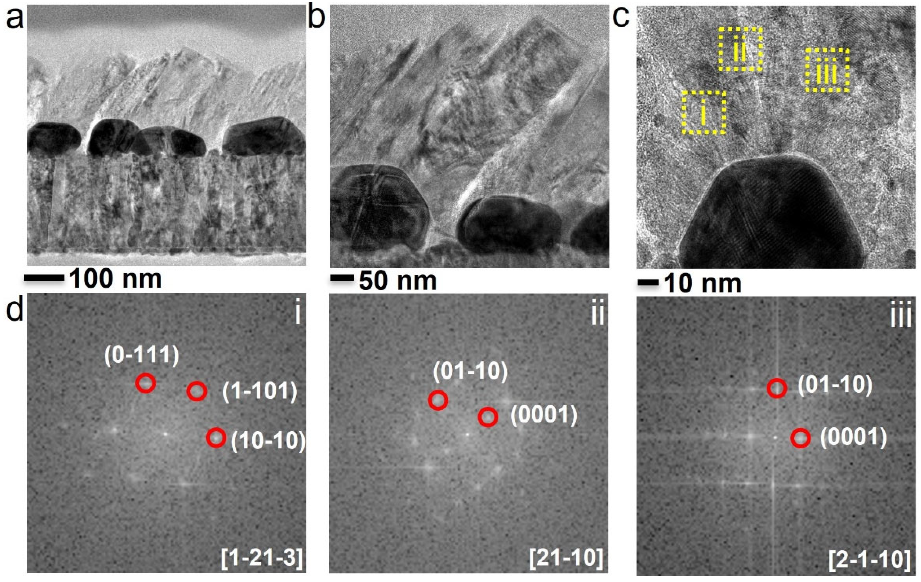
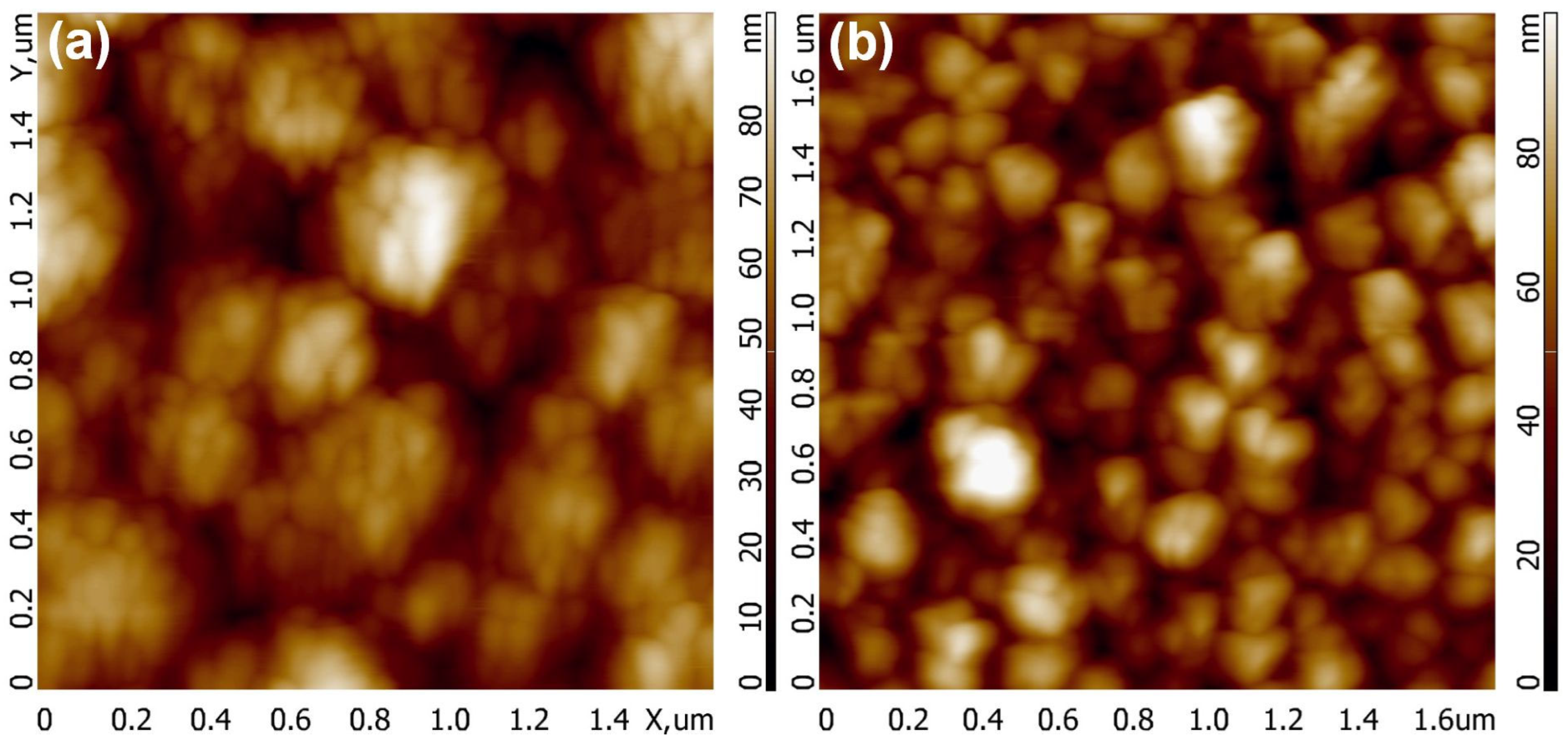
3. Results and Discussions
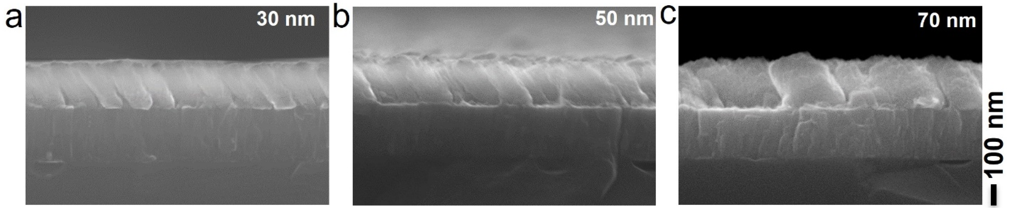
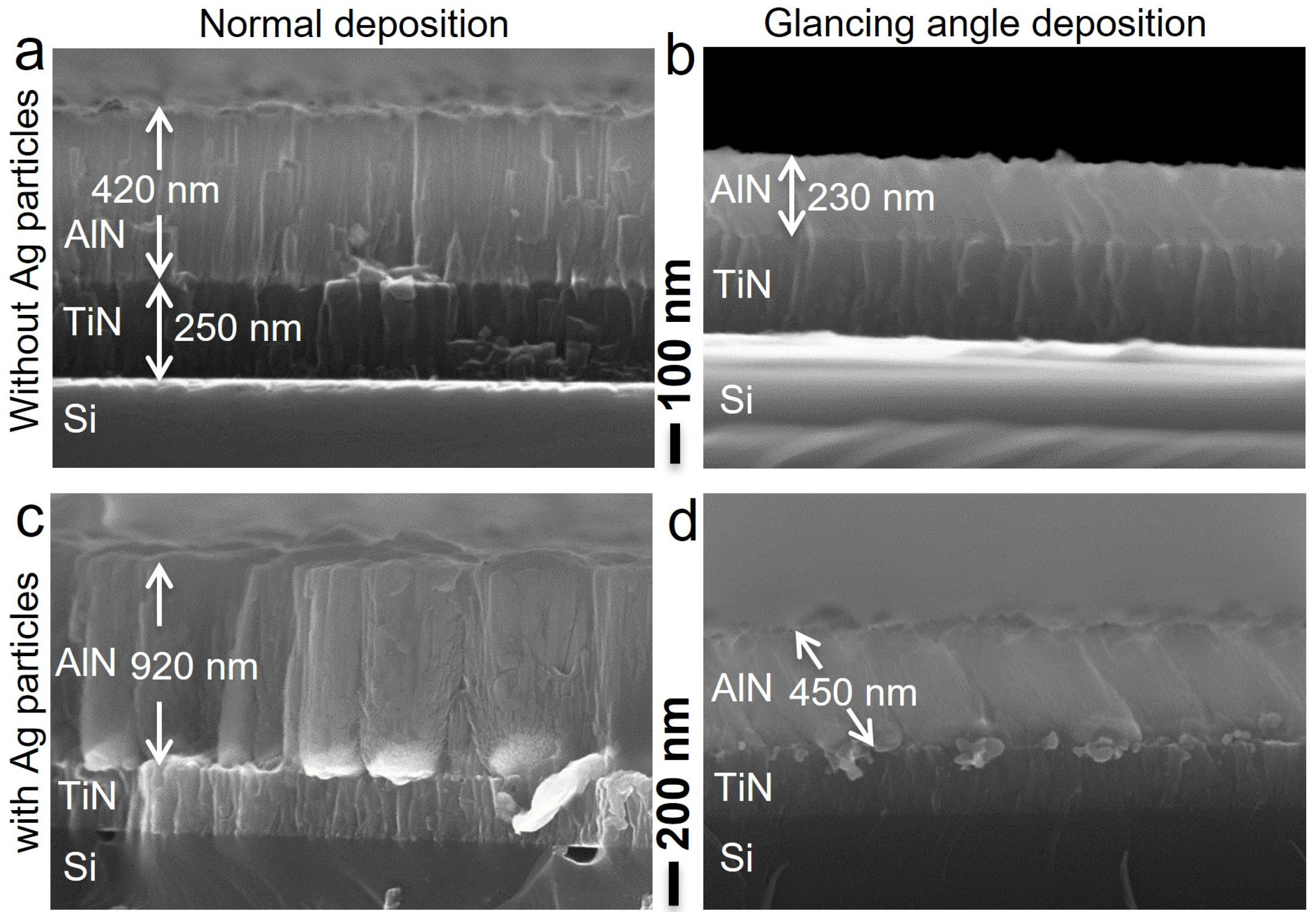
3.1. Dependence on Deposition Angle
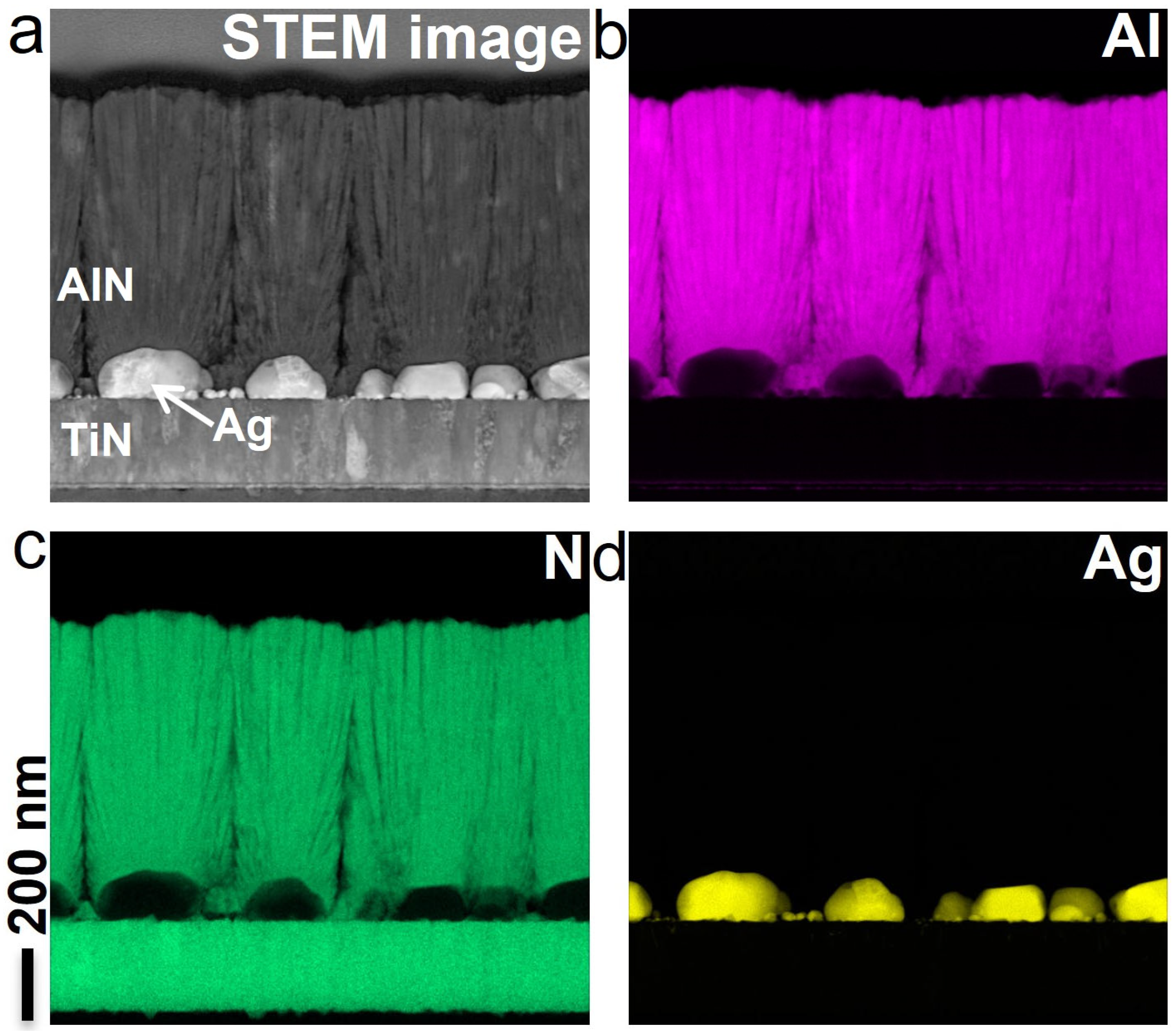
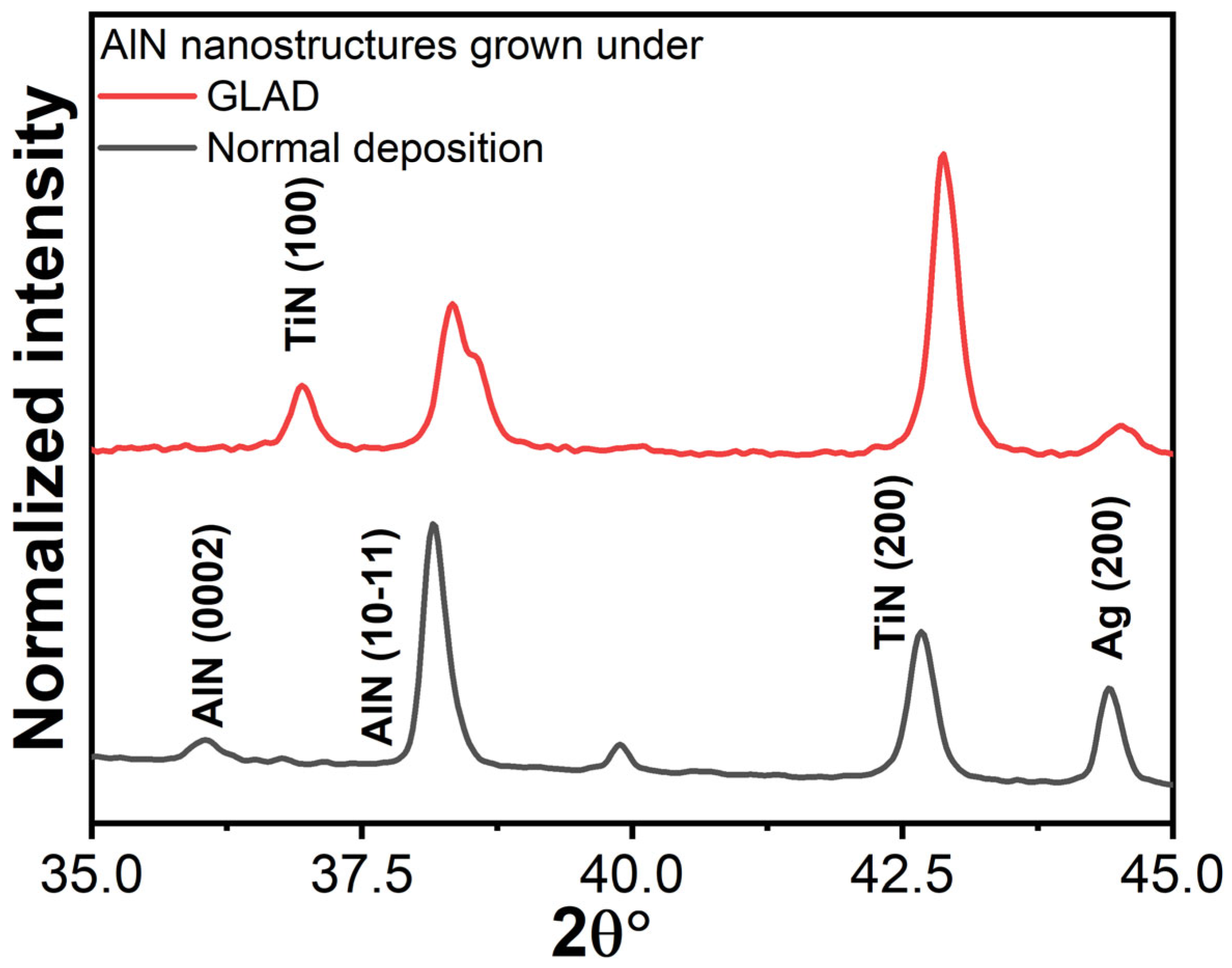
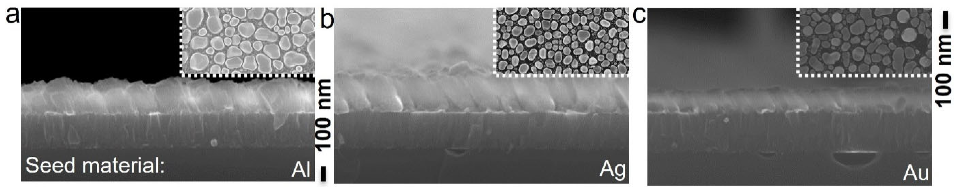
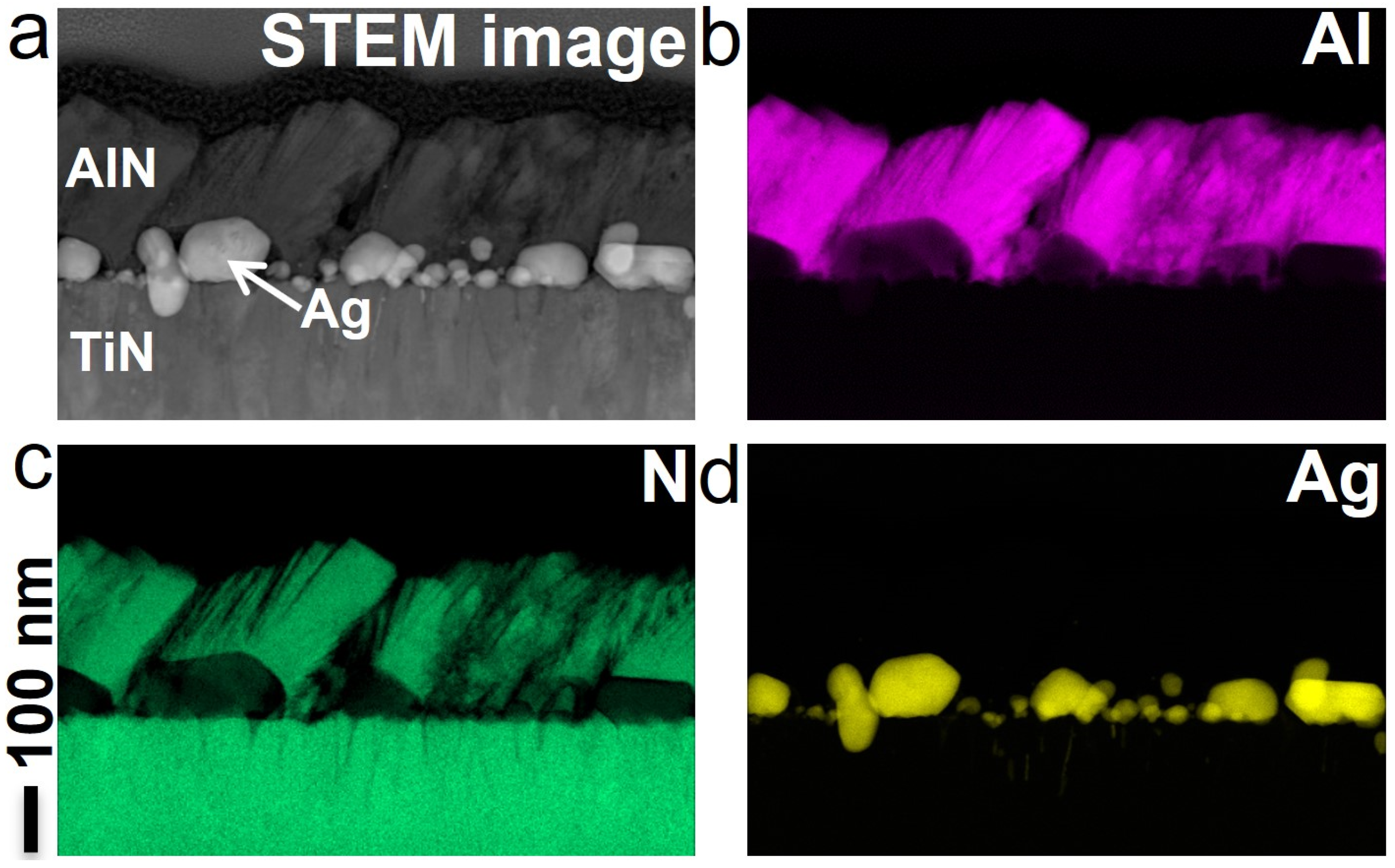
3.2. Dependence on Nanoparticle Material
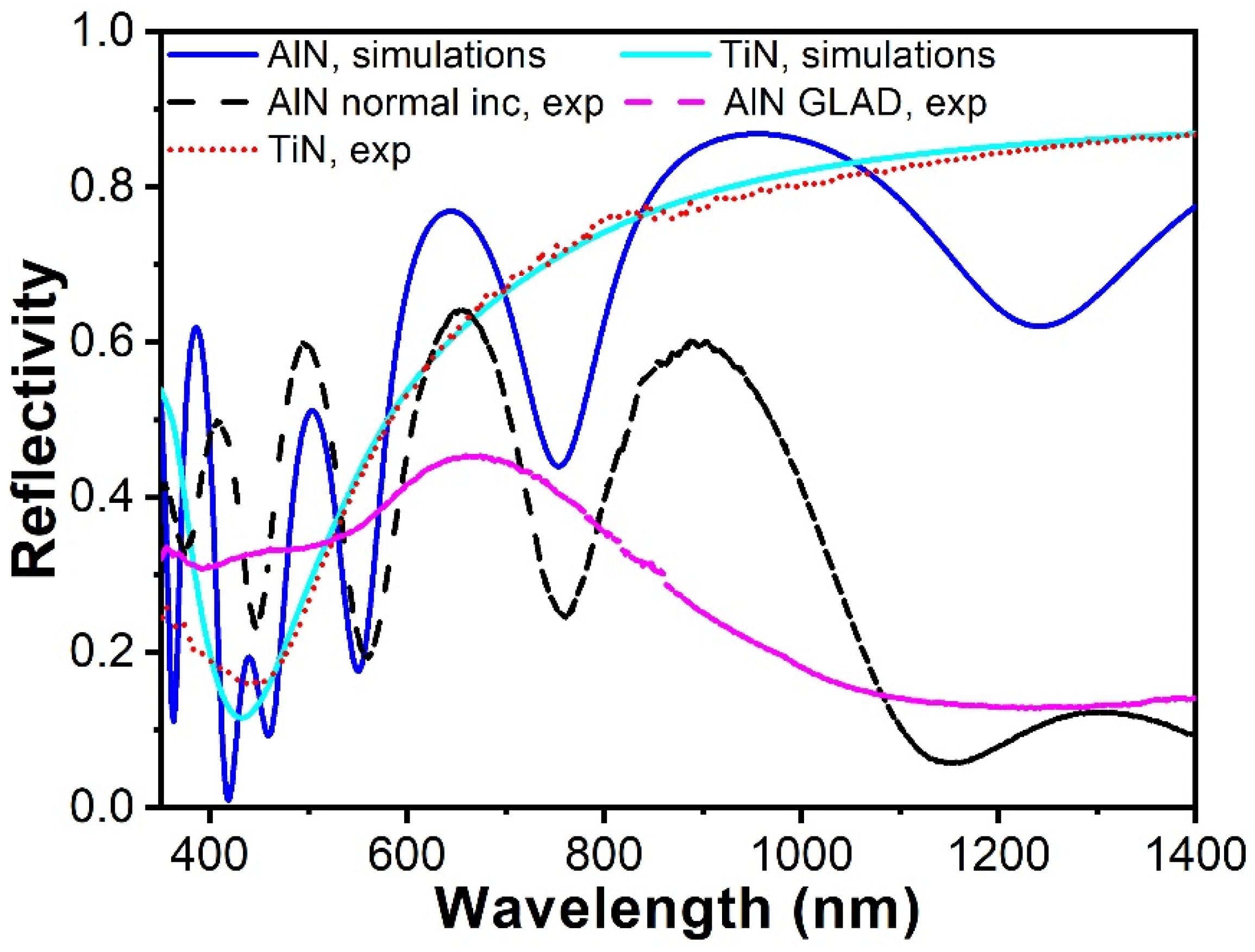
3.3. Linear Optical Characterization
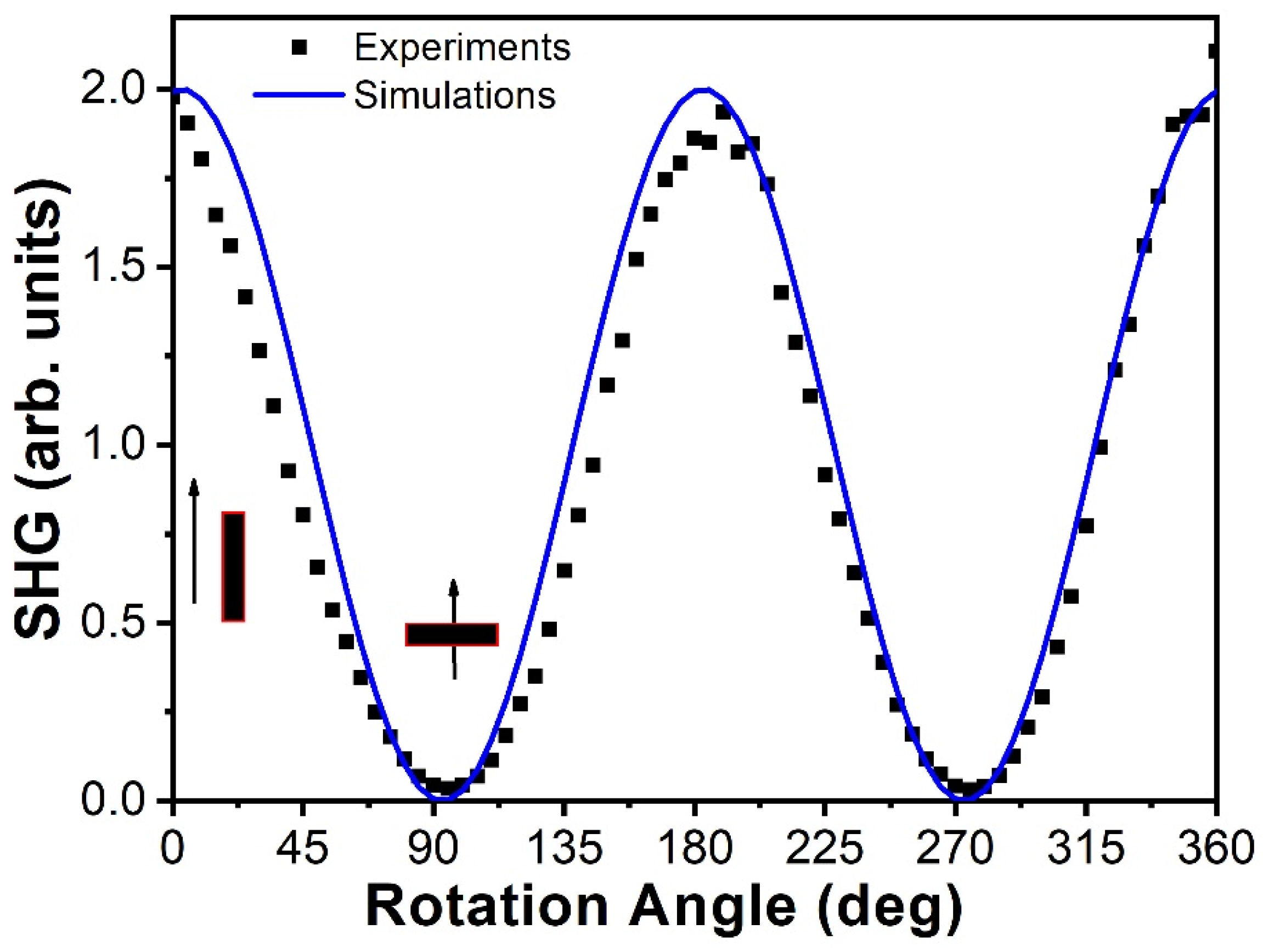
3.4. Second Harmonic Generation
4. Conclusions
Author Contributions
Funding
Data Availability Statement
Conflicts of Interest
References
- Liu, H.; Zhong, J.; Lee, C.; Lee, S.-W.; Lin, L. A comprehensive review on piezoelectric energy harvesting technology: Materials, mechanisms, and applications. Appl. Phys. Rev. 2018, 5, 041306. [Google Scholar] [CrossRef]
- Chen, F.; Ji, X.; Lau, S.P. Recent progress in group III-nitride nanostructures: From materials to applications. Mater. Sci. Eng. R Rep. 2020, 142, 100578. [Google Scholar] [CrossRef]
- Wu, Z.; Cheng, T.; Wang, Z.L. Self-Powered Sensors and Systems Based on Nanogenerators. Sensors 2020, 20, 2925. [Google Scholar] [CrossRef] [PubMed]
- Fei, C.; Liu, X.; Zhu, B.; Li, D.; Yang, X.; Yang, Y.; Zhou, Q. AlN piezoelectric thin films for energy harvesting and acoustic devices. Nano Energy 2018, 51, 146–161. [Google Scholar] [CrossRef]
- Wang, Z.L.; Song, J. Piezoelectric Nanogenerators Based on Zinc Oxide Nanowire Arrays. Science 2006, 312, 242–246. [Google Scholar] [CrossRef] [PubMed]
- Jamond, N.; Chrétien, P.; Houzé, F.; Lu, L.; Largeau, L.; Maugain, O.; Travers, L.; Harmand, J.C.; Glas, F.; Lefeuvre, E.; et al. Piezo-generator integrating a vertical array of GaN nanowires. Nanotechnology 2016, 27, 325403. [Google Scholar] [CrossRef] [PubMed]
- Gogneau, N.; Jamond, N.; Chrétien, P.; Houzé, F.; Lefeuvre, E.; Tchernycheva, M. From single III-nitride nanowires to piezoelectric generators: New route for powering nomad electronics. Semicond. Sci. Technol. 2016, 31, 103002. [Google Scholar] [CrossRef]
- Wang, X.; Song, J.; Liu, J.; Wang, Z.L. Direct-Current Nanogenerator Driven by Ultrasonic Waves. Science 2007, 316, 102–105. [Google Scholar] [CrossRef]
- Minary-Jolandan, M.; Bernal, R.A.; Espinosa, H.D. Strong piezoelectricity in individual GaN nanowires. MRS Commun. 2011, 1, 45–48. [Google Scholar] [CrossRef]
- Popok, V.N.; Chirumamilla, M.; Krekeler, T.; Ritter, M.; Pedersen, K. Magnetron Sputter Grown AlN Nanostructures with Giant Piezoelectric Response toward Energy Generation. ACS Appl. Nano Mater. 2023, 6, 8849–8856. [Google Scholar] [CrossRef]
- Agrawal, R.; Espinosa, H.D. Giant Piezoelectric Size Effects in Zinc Oxide and Gallium Nitride Nanowires. A First Principles Investigation. Nano Lett. 2011, 11, 786–790. [Google Scholar] [CrossRef] [PubMed]
- Kenry; Yong, K.-T.; Yu, S.F. AlN nanowires: Synthesis, physical properties, and nanoelectronics applications. J. Mater. Sci. 2012, 47, 5341–5360. [Google Scholar] [CrossRef]
- Nersisyan, H.H.; Lee, J.H.; Kim, H.Y.; Ryu, S.; Yoo, B.U. Morphological diversity of AlN nano- and microstructures: Synthesis, growth orientations and theoretical modelling. Int. Mater. Rev. 2020, 65, 323–355. [Google Scholar] [CrossRef]
- Dong, J.; Chen, L.; Yang, Y.; Wang, X. Piezotronic effect in AlGaN/AlN/GaN heterojunction nanowires used as a flexible strain sensor. Beilstein J. Nanotechnol. 2020, 11, 1847–1853. [Google Scholar] [CrossRef] [PubMed]
- Yazdi, G.R.; Persson, P.O.Å.; Gogova, D.; Fornari, R.; Hultman, L.; Syväjärvi, M.; Yakimova, R. Aligned AlN nanowires by self-organized vapor–solid growth. Nanotechnology 2009, 20, 495304. [Google Scholar] [CrossRef] [PubMed]
- Jaloustre, L.; Le Denmat, S.; Auzelle, T.; Azadmand, M.; Geelhaar, L.; Dahlem, F.; Songmuang, R. Toward Quantitative Measurements of Piezoelectricity in III-N Semiconductor Nanowires. ACS Appl. Nano Mater. 2021, 4, 43–52. [Google Scholar] [CrossRef]
- Mwema, F.M.; Akinlabi, E.T.; Oladijo, O.P. A systematic review of magnetron sputtering of AlN thin films for extreme condition sensing. Mater. Today Proc. 2020, 26, 1546–1550. [Google Scholar] [CrossRef]
- Jiao, X.; Shi, Y.; Zhong, H.; Zhang, R.; Yang, J. AlN thin films deposited on different Si-based substrates through RF magnetron sputtering. J. Mater. Sci. Mater. Electron. 2015, 26, 801–808. [Google Scholar] [CrossRef]
- Peng, M.Z.; Guo, L.W.; Zhang, J.; Yu, N.S.; Zhu, X.L.; Yan, J.F.; Wang, Y.; Jia, H.Q.; Chen, H.; Zhou, J.M. Effect of growth temperature of initial AlN buffer on the structural and optical properties of Al-rich AlGaN. J. Cryst. Growth 2007, 307, 289–293. [Google Scholar] [CrossRef]
- Shin, I.-S.; Kim, J.; Lee, D.; Kim, D.; Park, Y.; Yoon, E. Epitaxial growth of single-crystalline AlN layer on Si(111) by DC magnetron sputtering at room temperature. Jpn. J. Appl. Phys. 2018, 57, 060306. [Google Scholar] [CrossRef]
- Pingen, K.; Neuhaus, S.; Wolff, N.; Kienle, L.; Žukauskaitė, A.; von Hauff, E.; Hinz, A.M. Influence of Si(111) substrate off-cut on AlN film crystallinity grown by magnetron sputter epitaxy. J. Appl. Phys. 2023, 134, 025304. [Google Scholar] [CrossRef]
- Riah, B.; Camus, J.; Ayad, A.; Rammal, M.; Zernadji, R.; Rouag, N.; Djouadi, M.A. Hetero-Epitaxial Growth of AlN Deposited by DC Magnetron Sputtering on Si(111) Using a AlN Buffer Layer. Coatings 2021, 11, 1063. [Google Scholar] [CrossRef]
- Depla, D.; Dedoncker, R.; Strijckmans, K. Nitride formation during reactive sputter deposition of multi-principal element alloys in argon/nitrogen mixtures. Thin Solid Film. 2021, 732, 138721. [Google Scholar] [CrossRef]
- Iriarte, G.F.; Rodríguez, J.G.; Calle, F. Synthesis of c-axis oriented AlN thin films on different substrates: A review. Mater. Res. Bull. 2010, 45, 1039–1045. [Google Scholar] [CrossRef]
- Sandager, M.K.; Kjelde, C.; Popok, V. Growth of Thin AlN Films on Si Wafers by Reactive Magnetron Sputtering: Role of Processing Pressure, Magnetron Power and Nitrogen/Argon Gas Flow Ratio. Crystals 2022, 12, 1379. [Google Scholar] [CrossRef]
- Reusch, M.; Holc, K.; Pletschen, W.; Kirste, L.; Žukauskaitė, A.; Yoshikawa, T.; Iankov, D.; Ambacher, O.; Lebedev, V. Analysis and optimization of sputter deposited AlN-layers for flexural plate wave devices. J. Vac. Sci. Technol. B 2016, 34, 052001. [Google Scholar] [CrossRef]
- Iqbal, A.; Mohd-Yasin, F. Reactive Sputtering of Aluminum Nitride (002) Thin Films for Piezoelectric Applications: A Review. Sensors 2018, 18, 1797. [Google Scholar] [CrossRef]
- Marauska, S.; Dankwort, T.; Quenzer, H.J.; Wagner, B. Sputtered thin film piezoelectric aluminium nitride as a functional MEMS material and CMOS compatible process integration. Procedia Eng. 2011, 25, 1341–1344. [Google Scholar] [CrossRef]
- Barranco, A.; Borras, A.; Gonzalez-Elipe, A.R.; Palmero, A. Perspectives on oblique angle deposition of thin films: From fundamentals to devices. Prog. Mater. Sci. 2016, 76, 59–153. [Google Scholar] [CrossRef]
- Bairagi, S.; Järrendahl, K.; Eriksson, F.; Hultman, L.; Birch, J.; Hsiao, C.-L. Glancing Angle Deposition and Growth Mechanism of Inclined AlN Nanostructures Using Reactive Magnetron Sputtering. Coatings 2020, 10, 768. [Google Scholar] [CrossRef]
- Krekeler, T.; Rout, S.S.; Krishnamurthy, G.V.; Störmer, M.; Arya, M.; Ganguly, A.; Sutherland, D.S.; Bozhevolnyi, S.I.; Ritter, M.; Pedersen, K.; et al. Unprecedented Thermal Stability of Plasmonic Titanium Nitride Films up to 1400 °C. Adv. Opt. Mater. 2021, 9, 2100323. [Google Scholar] [CrossRef]
- Di Pietrantonio, F.; Fosca, M.; Benetti, M.; Cannatà, D.; Verona, C.; Teghil, R.; De Bonis, A.; Rau, J.V. Flower-like aluminium nitride nanostructures deposited by rf magnetron sputtering on superhard rhodium boride films. Appl. Phys. A 2019, 125, 681. [Google Scholar] [CrossRef]
- Ji, X.; Li, H.; Wu, Z.; Cheng, S.; Hu, H.; Yan, D.; Zhuo, R.; Wang, J.; Yan, P. Growth of AlN hexagonal oriented complex nanostructures induced by nucleus arrangement. CrystEngComm 2011, 13, 5198–5203. [Google Scholar] [CrossRef]
- Azadmand, M.; Auzelle, T.; Lähnemann, J.; Gao, G.; Nicolai, L.; Ramsteiner, M.; Trampert, A.; Sanguinetti, S.; Brandt, O.; Geelhaar, L. Self-Assembly of Well-Separated AlN Nanowires Directly on Sputtered Metallic TiN Films. Phys. Status Solidi (RRL) Rapid Res. Lett. 2020, 14, 1900615. [Google Scholar] [CrossRef]
- Chen, L.-C.; Tien, C.-H.; Chien, S.-Y.; Liao, W.-C.; Huang, C.-C.; Mu, C.-S.; Chen, C.-C.; Hsu, Y.-Y. A nanorods AlN layer prepared by sputtering at oblique-angle and application as a buffer layer in a GaN-based light emitting diodes. Proc. SPIE 2010, 7784, 778417. [Google Scholar]
- Wu, Y.; Yang, P. Direct Observation of Vapor−Liquid−Solid Nanowire Growth. J. Am. Chem. Soc. 2001, 123, 3165–3166. [Google Scholar] [CrossRef]
- Trentler, T.J.; Hickman, K.M.; Goel, S.C.; Viano, A.M.; Gibbons, P.C.; Buhro, W.E. Solution-Liquid-Solid Growth of Crystalline III-V Semiconductors: An Analogy to Vapor-Liquid-Solid Growth. Science 1995, 270, 1791–1794. [Google Scholar] [CrossRef]
- Yu, L.; Hu, Z.; Ma, Y.; Huo, K.; Chen, Y.; Sang, H.; Lin, W.; Lu, Y. Evolution of aluminum nitride nanostructures from nanoflower to thin film on silicon substrate by direct nitridation of aluminum precursor. Diam. Relat. Mater. 2007, 16, 1636–1642. [Google Scholar] [CrossRef]
- Jiang, R.; Meng, X. Synthesis of aluminum nitride nanostructures via chemical vapor deposition method with nickel as catalyst. Rev. Mex. Física 2018, 64, 67–71. [Google Scholar] [CrossRef]
- Yu, L.; Lv, Y.; Zhang, X.; Zhang, Y.; Zou, R.; Zhang, F. Vapor–liquid–solid growth route to AlN nanowires on Au-coated Si substrate by direct nitridation of Al powder. J. Cryst. Growth 2011, 334, 57–61. [Google Scholar] [CrossRef]
- Reddy, H.; Guler, U.; Kudyshev, Z.; Kildishev, A.V.; Shalaev, V.M.; Boltasseva, A. Temperature-Dependent Optical Properties of Plasmonic Titanium Nitride Thin Films. ACS Photonics 2017, 4, 1413–1420. [Google Scholar] [CrossRef]
- Antoine-Vincent, N.; Natali, F.; Mihailovic, M.; Vasson, A.; Leymarie, J.; Disseix, P.; Byrne, D.; Semond, F.; Massies, J. Determination of the refractive indices of AlN, GaN, and AlxGa1−xN grown on (111)Si substrates. J. Appl. Phys. 2003, 93, 5222–5226. [Google Scholar] [CrossRef]
- Blanc, D.; Cachard, A.; Pommier, J. All-optical probing of material structure by second harmonic generation: Application to piezoelectric aluminium nitride thin films. Opt. Eng. 1997, 36, 1191–1195. [Google Scholar] [CrossRef]


Disclaimer/Publisher’s Note: The statements, opinions and data contained in all publications are solely those of the individual author(s) and contributor(s) and not of MDPI and/or the editor(s). MDPI and/or the editor(s) disclaim responsibility for any injury to people or property resulting from any ideas, methods, instructions or products referred to in the content. |
© 2023 by the authors. Licensee MDPI, Basel, Switzerland. This article is an open access article distributed under the terms and conditions of the Creative Commons Attribution (CC BY) license (https://creativecommons.org/licenses/by/4.0/).
Share and Cite
Chirumamilla, M.; Krekeler, T.; Wang, D.; Kristensen, P.K.; Ritter, M.; Popok, V.N.; Pedersen, K. Magnetron Sputter Deposition of Nanostructured AlN Thin Films. Appl. Nano 2023, 4, 280-292. https://doi.org/10.3390/applnano4040016
Chirumamilla M, Krekeler T, Wang D, Kristensen PK, Ritter M, Popok VN, Pedersen K. Magnetron Sputter Deposition of Nanostructured AlN Thin Films. Applied Nano. 2023; 4(4):280-292. https://doi.org/10.3390/applnano4040016
Chicago/Turabian StyleChirumamilla, Manohar, Tobias Krekeler, Deyong Wang, Peter K. Kristensen, Martin Ritter, Vladimir N. Popok, and Kjeld Pedersen. 2023. "Magnetron Sputter Deposition of Nanostructured AlN Thin Films" Applied Nano 4, no. 4: 280-292. https://doi.org/10.3390/applnano4040016
APA StyleChirumamilla, M., Krekeler, T., Wang, D., Kristensen, P. K., Ritter, M., Popok, V. N., & Pedersen, K. (2023). Magnetron Sputter Deposition of Nanostructured AlN Thin Films. Applied Nano, 4(4), 280-292. https://doi.org/10.3390/applnano4040016