Article

Comparative Study of Printed Multilayer OLED Fabrication through Slot Die Coating, Gravure and Inkjet Printing, and Their Combination

1
Institute of Thermal Process Engineering, Thin Film Technology, Karlsruhe Institute of Technology (KIT), Kaiserstrasse 12, 76131 Karlsruhe, Germany
2
InnovationLab (iL), Speyerer Strasse 4, 69115 Heidelberg, Germany
3
Institute of Printing Science and Technology, TU Darmstadt, Magdalenenstrasse 2, 64289 Darmstadt, Germany
4
Light Technology Institute, Karlsruhe Institute of Technology (KIT), Kaiserstrasse 12, 76131 Karlsruhe, Germany
5
Department of Chemistry, University of Cologne, Luxemburger Strasse 116, 50939 Cologne, Germany
6
COPT Center for Organic Electron, University of Cologne, Luxemburger Strasse, 90, 50939 Cologne, Germany
7
ZOEK Zentrum für Organische Elektronik Köln gGmbH, Luxemburger Strasse 90, 50939 Cologne, Germany
*
Authors to whom correspondence should be addressed.
Colloids Interfaces 2019, 3(1), 32; https://doi.org/10.3390/colloids3010032
Submission received: 31 January 2019 / Revised: 28 February 2019 / Accepted: 3 March 2019 / Published: 6 March 2019
(This article belongs to the Special Issue Colloids and Interfaces in Printing Technology)

Abstract

:
In this study, multilayer organic light-emitting diodes (OLEDs) consisting of three solution-processed layers are fabricated using slot die coating, gravure printing, and inkjet printing, techniques that are commonly used in the industry. Different technique combinations are investigated to successively deposit a hole injection layer (poly(3,4-ethylenedioxythiophene)-poly(styrenesulfonate) (PEDOT:PSS)), a cross-linkable hole transport layer (N,N′-bis(4-(6-((3-ethyloxetan-3-yl)methoxy)-hexyloxy)phenyl)-N,N′-bis(4-methoxyphenyl)biphenyl-4,4′-diamin (QUPD)), and a green emissive layer (TSG-M) on top of each other. In order to compare the application techniques, the ink formulations have to be adapted to the respective process requirements. First, the influence of the application technique on the layer homogeneity of the different materials is investigated. Large area thickness measurements of the layers based on imaging color reflectometry (ICR) are used to compare the application techniques regarding the layer homogeneity and reproducible film thickness. The total stack thickness of all solution-processed layers of 32 OLEDs could be reproduced homogeneously in a process window of 30 nm for the technique combination of slot die coating and inkjet printing. The best efficiency of 13.3 cd A−1 is reached for a process combination of slot die coating and gravure printing. In order to enable a statistically significant evaluation, in total, 96 OLEDs were analyzed and the corresponding 288 layers were measured successively to determine the influence of layer homogeneity on device performance.

Graphical Abstract

1. Introduction

Organic electronic devices such as thin-film-transistors (TFTs) as well as organic light-emitting diodes (OLEDs) for display and lighting applications are increasingly available for the end consumer. However, they are still an expensive choice [1]. A reason for this is that most of the devices on the market are produced by thermal evaporation in high vacuum. The evaporation process is well-suited to realize the required complex multilayer architecture but is disadvantageous in terms of material loss and throughput. Furthermore, the purchase and operation costs of the used equipment are high. Solution processing allows both the usability of small molecules as well as polymers and the manufacturing of large area devices using continuous roll-to-roll (R2R) processes [2,3]. Spin coating is a commonly used lab scale technique for the deposition of organic electronic materials from solution because it offers easy handling and because different formulations can be investigated quickly [4,5,6]. Of large interest are application techniques with low material loss, which provide the possibility of large-area films and continuous operation [4]. The production of organic electronics with industry-relevant techniques requires, in addition to the chemical and physical understanding of the ink formulation, the knowledge of the technical process requirements [6]. Søndergaard et al. and Krebs [6,7] give an overview about the different roll-to-roll coating and printing techniques for the production of organic thin films and devices. To the best of our knowledge, there are no previous comparative works, where a qualitative and quantitative comparison of the application of different industrial solution processes and techniques for the fabrication of OLEDs, which also includes device performance investigation, are reported.
In this work, we focus on the suitability of three coating and printing techniques for the production of large-area solution-processed multilayer OLEDs. These OLEDs were fabricated with three individual solution-processed layers, consisting of the commonly used Poly(3,4-ethylenedioxythiophene)-poly(styrenesulfonate) (PEDOT:PSS) as a hole injection layer (HIL), followed by two layers based on small molecules that serve as a hole transport layer (HTL) and an emissive layer (EML) respectively. The cross-linkable material N,N′-bis(4-(6-((3-ethyloxetan-3-yl)methoxy)-hexyloxy)phenyl)-N,N′-bis(4-methoxyphenyl)biphenyl-4,4′-diamin (QUPD) is used for the HTL, since the cross-linking of this material allows the generation of a solvent resistant layer. Therefore, the identical solvent used for the HTL can also be used to deposit the subsequent emissive TSG-M layer. For the production of these solution-processed multilayer OLEDs, the suitability of the high-throughput application techniques of slot die coating, gravure printing, and inkjet printing as well as combinations of those were investigated, since these techniques can be easily scaled-up and operated continuously [7]. The application of large-area homogeneous layers with a precisely controlled thickness of a few nanometers is a crucial step in the successful production of organic electronic devices. In order to avoid undesired film inhomogeneities caused by de-wetting effects or crystallization, the influences of the processing parameters, ink formulation, and posttreatment methods have to be considered and adjusted to the respective application technique. Since the reproducible adjustment of the layer thickness represents a sensitive parameter, the three application techniques were compared in terms of film homogeneity for each of the three materials, which were evaluated via Imaging Color Reflectometry (ICR) and regarding device performance. The ink formulations were adjusted to the boundary conditions specified by the respective printing technique. Since each technique has different requirements for the ink formulation, it was investigated whether the best performance of a solution-processed multilayer OLED can be achieved with a process combination for the different layers.

1.1. State of the Art of Printed Multilayer OLEDs

Due to the multiple difficulties in the solution processing of multilayer OLEDs, there are only a few studies on OLEDs consisting exclusively of solution-processed functional layers. One of the key challenges is to apply layers with precise thicknesses in the nm-range homogeneously on cm2-sized areas. It has to be considered that the thickness of the layers and the position of the recombination zone (where the photons are generated) are crucial parameters. Any significant change of the total device thickness or position of the recombination zone can affect the emission spectrum of the device due to cavity effects as well as device efficiency [8]. To transfer the OLED production from lab-scale to industry-scale, it is necessary to achieve homogeneous layers with industry relevant coating or printing techniques. Therefore, process specific requirements have to be considered for the ink formulation, which will be discussed in more detail afterwards. A good wetting behaviour of the ink on the substrate (the bottom layer) is a basic prerequisite for a homogeneous layer formation independent of the application technique. On the one hand, oxygen or argon plasma as a pretreatment step to increase the surface energy of the substrate is widely spread and is commonly used in literature [9,10,11]. On the other hand, wettability can be improved by reducing the surface tension of the ink by adding surfactants, such as Triton-X for water-based formulations [12,13]. The material class of small molecules is particularly interesting due to the higher efficiency compared to polymers but also more challenging regarding solution processing [14]. In extreme cases, crystallization effects can occur during the drying process of small molecule films, resulting in short-circuit phenomena. Simultaneously, pinhole-like surfaces can be formed, which affect the performance of the devices [14]. Choi et al. [12,15] produced green multilayer OLEDs with two slot-die-coated layers, PEDOT:PSS as an HIL and a small molecule HTL. In order to prevent a pinhole-like surface and to obtain a homogeneous HTL, the functional polymer Poly(9-vinylcarbazole) (PVK) was added to the ink formulation. Thus, the average roughness value of 122 nm for a pure small molecule layer could be reduced to a value of 0.6 nm for the hybrid layer [15]. However, three additional functional layers were evaporated, resulting in devices with an efficiency up to 27.2 lm W−1 [12]. The second key challenge in the fabrication of solution-processed multilayers is to avoid the dissolution of the previously dried bottom layer when applying a wet film on top of it and, consequently, the intermixing of solids. For a successful separation of the functional layers and, thus, highly efficient devices, different concepts are available in the literature. The most common are the orthogonal solvent approach and the use of cross-linkable materials. Regarding the orthogonal solvent approach, the new layer solvents used have a very low solubility for the material of the previous layer in order not to dissolve it [16]. In previous works, we have already been able to show that this approach can successfully separate three slot-die-coated layers, which led to an increase in efficiency by a factor of 42 compared to two-layer OLEDs. Abbel et al. [17] fabricated slot-die-coated green OLEDs in the R2R mode, consisting of a HIL and a green polymer EML, using the orthogonal solvent approach. The achieved efficiency was comparable to the sheet-to-sheet (S2S) fabricated OLEDs with 5–7 cd A−1, proving that the technique is suitable on an industrial scale. Choi et al. [15] mentioned that the addition of polymers to small molecule inks has a positive effect on the prevention of layer intermixing due to the higher molecular weight and thus lower mobility. State of the art gravure-printed devices consist of two layers: PEDOT:PSS and an emissive layer. Chung et al. [9] achieved efficiencies up to 8.8 lm W−1 with a gravure-printed polymer EML, which was almost equal to the value achieved by spin coating. Therefore, a blend of a low and high boiling point organic solvent was used to ensure the substrate wetting and film stability during drying [9]. Tekoglu et al. [18] also produced gravure-printed OLEDs consisting of PEDOT:PSS and a green small molecule emitter, resulting in a maximum efficiency of 7.7 cd A−1. Inkjet printing as a deposition technique for a variety of layers of OLEDs including HIL [19], EML [20], and EIL [21] has been extensively studied. In recent years, the focus has shifted to the deposition of thermally activated delayed fluorescence (TADF) emitters for display applications. Due to the new material class, efficiencies of more than 45 cd A−1 have been achieved with an inkjet-printed TADF emitter and three further evaporated layers [22].
In particular, when combining different techniques to fabricate the functional layers of a multilayer OLED, special issues like substrate contamination or substrate alignment have to be considered in addition to the general challenges of solution processing.

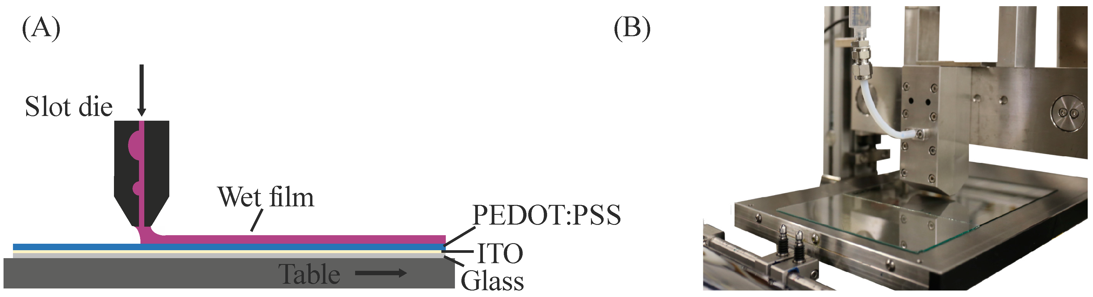
1.2. Slot Die Coating

Slot die coating is a pre-metered coating technique; this means the required wet film thickness can be adjusted directly via setting a defined volume flow for a certain coating speed and width. The coating ink is pumped through the slot die head and distributed across the coating width. As it can be seen in Figure 1, the substrate table moves under the fixed slot die at a continuous speed. The application method is suitable for a wide range of viscosities, from high viscous battery slurries with values up to 1000 mPa⋅s [23] to low viscosity solutions, which behave like pure solvents [24]. Another advantage of this application technique is the possibility to produce structured coatings like patches or stripes as well as simultaneous multilayer coatings [17,25,26,27,28]. Some limiting factors and film defect sources need to be taken into consideration in order to optimize the application process. For wet film thicknesses below a critical value at a certain speed, the liquid bridge in the gap between lip and substrate becomes unstable, resulting in coating defects [29,30]. If the coating is not applied continuously but in a S2S mode, it has to be considered that it takes a few seconds until the coating solution has bridged the gap between slot die and substrate and until a state of equilibrium between the delivered and applied volume is reached [12]. In order to achieve a steady-state mode as quickly as possible, the substrate movement can be started delayed to the pumping process; additionally, the inlet zone can be extended (if possible) or glass instead of plastic syringes may be used [13,31]. Otherwise, a layer thickness gradient in the coating direction can occur; for example a thickness increase from 66 nm to 88 nm was observed for a slot-die-coated green emissive material over a coating length of 131 mm [13]. In addition to coating defects, nonuniform thickness variations may also occur due to inhomogeneous drying conditions, especially when solvent mixtures are used as we have already reported for PEDOT:PSS layers [13]. In previous publications, the authors have already investigated slot die coating as a scalable technique to manufacture solution-processed multilayer OLEDs using different material classes with reproducible performance [13,31,32]. In the publication of Raupp et al. [13], flexographic printing and slot die coating were directly compared to produce green OLEDs with two solution-processed layers.

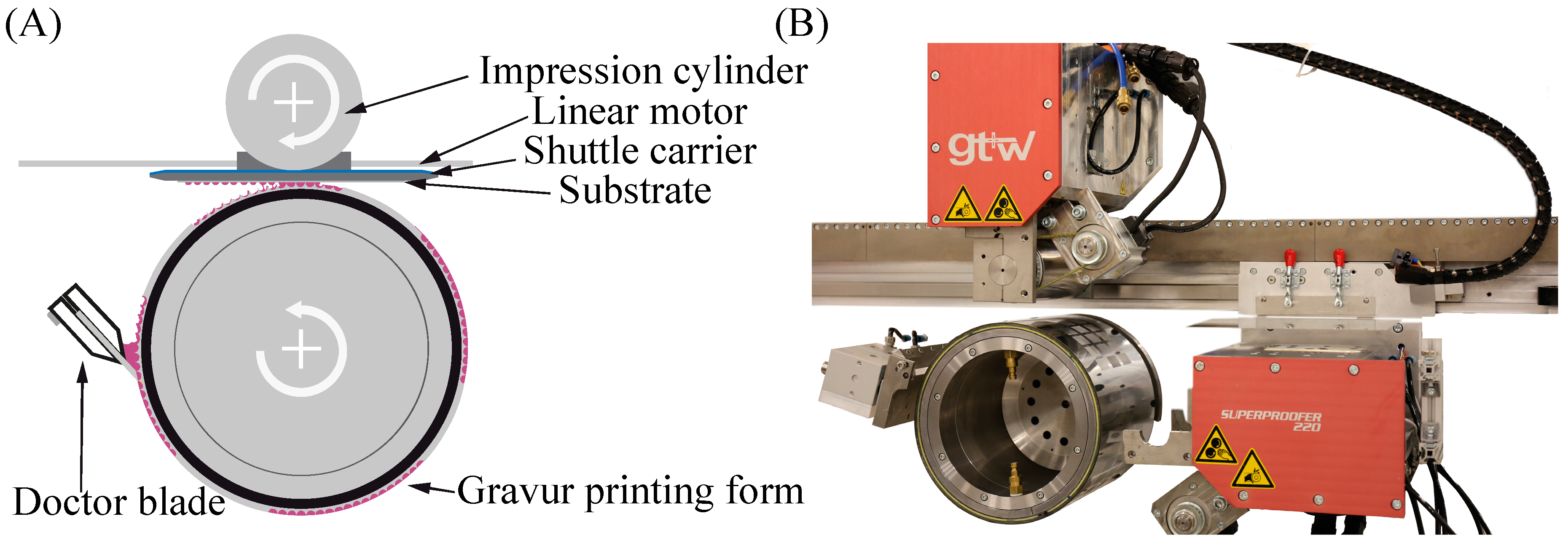
1.3. Gravure Printing

In contrast to slot die coating, gravure printing allows the printing of small structures in the range of micrometers as well as the application of large area functional layers with a size of several cm2. Due to its high throughput [33], it is also suitable for the mass production of printed electronics. The printing process may be split into a pre-dosing, a dosing, a transfer, and a drying phase. When pre-dosing, the fluid is applied on the surface of the printing form cylinder. As the cylinder rotates, the excess ink is wiped off by the clinging doctor blade and the engraved cells of the gravure cylinder are filled with ink (Figure 2). In a next phase, the substrate carrier including the substrate itself is moved over the printing cylinder. Therefore, the impression cylinder presses the substrate against the printing cylinder. In order to minimize slip, the substrate carrier and the printing cylinder are adjusted to the same velocity before getting into contact. The amount of ink transferred in one printing run ranges from 30% to 70%, whereas the rest of the ink stays in the engraved cells and is refilled in the following turn [34]. One can distinguish between two different ink transfer regimes, which are mainly influenced by the fluid properties of the ink and the gravure parameters of the cylinder. The first regime is dominated by single dot splitting. Each engraved cell develops an individual capillary bridge to the substrate. Consequently, each cell eventually corresponds to a specific defined drop on the substrate. In order to evolve a homogenous layer, the individual drops are required to spread and coalesce on the substrate before drying. The second regime involves the formation of a fluid meniscus between adjacent cells of the printing cylinder and the substrate. Instead of individual cells, a fluid meniscus as wide as the engraved space is being transferred. The advantage of depositing an already closed layer is cut back by additional hydrodynamic instabilities. The advancing line of contact on the substrate is susceptible to the viscous fingering instability, a variation of the Saffman–Taylor–Couette flow instability [35,36,37]. It leads to a periodic perturbation of the layer thickness perpendicular to the printing direction. In order to evolve homogenous layers, the drying time of the layer has to exceed the leveling time of the perturbations. The production of gravure printed small molecule OLEDs (SMOLEDs) is a major challenge due to the low viscosity of the inks and the aggregation of the small molecules during the drying process [18]. Tekoglu et al. [18] added polystyrene to the ink formulation to increase the viscosity to a value of 6 mPa⋅s, whereas the value of the pure small molecule ink was less than 2 mPa⋅s. Despite the addition of insulating PS, an efficiency increase of 67% could be achieved due to the more homogeneous film formation compared to the small molecule reference device [18].

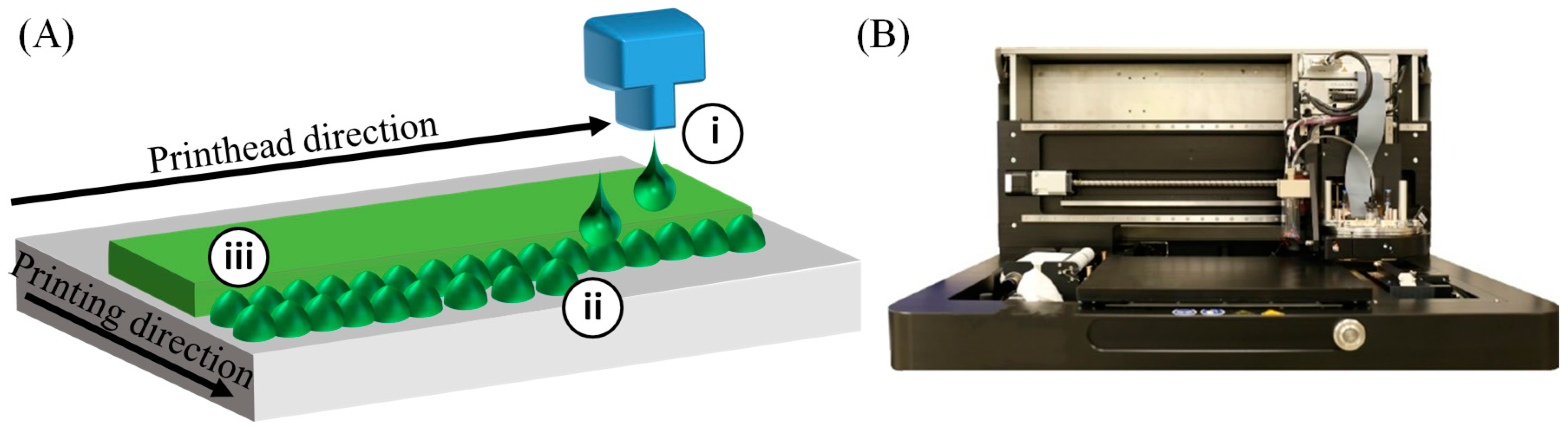
1.4. Inkjet Printing

In the commonly used drop-on-demand (DOD) inkjet printing systems, the ink is only deposited when it is actually desired. This results in a very low waste of material [38,39]. Due to its digital nature, inkjet printing allows the highest flexibility in terms of shape of the printed patterns, compared to the techniques mentioned above. The printing pattern can be easily changed or adjusted by changing the template [40,41]. Inkjet printing, as well as slot die coating, is a noncontact printing technique, and there are almost no limitations regarding the substrate; plastics, foils, glass, or textiles can be used [42,43,44]. However, the drawbacks are the special requirements and restrictions regarding the physical properties of the ink. As a general rule, the viscosity should range from 1 to 25 mPa⋅s, and the surface tension should range from 25 to 50 mN m−1 [38,39,45]. The printing process itself can be separated into three subsequent phases: (i) droplet ejection, (ii) droplet deposition, and (iii) film formation and drying, as shown in Figure 3. Depending on the printing strategy, all these individual steps can cause a variety of printing defects. Besides a not optimized wettability, the most common defect in inkjet printing is the so-called coffee-stain effect, which is particularly relevant for the printing of small structures and thin films. The edge of the printed layer develops a wall which is significantly protruding over its center level [46]. If individual nozzles clog during printing, this can lead to perforated layers, resulting in a failure of the devices. For low viscosity values, for example when pure toluene is used as solvent, the controlled drop ejection is difficult, resulting in misdirected and irregular jets and, thus, misplaced structures or saw tooth-like edges [19]. Olivier et al. [19] used solvents of a higher viscosity such as anisole and isopropanol in addition to toluene to adjust the rheological behavior of a small molecule ink.

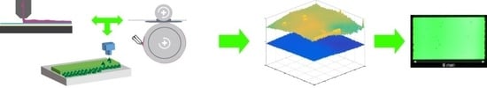
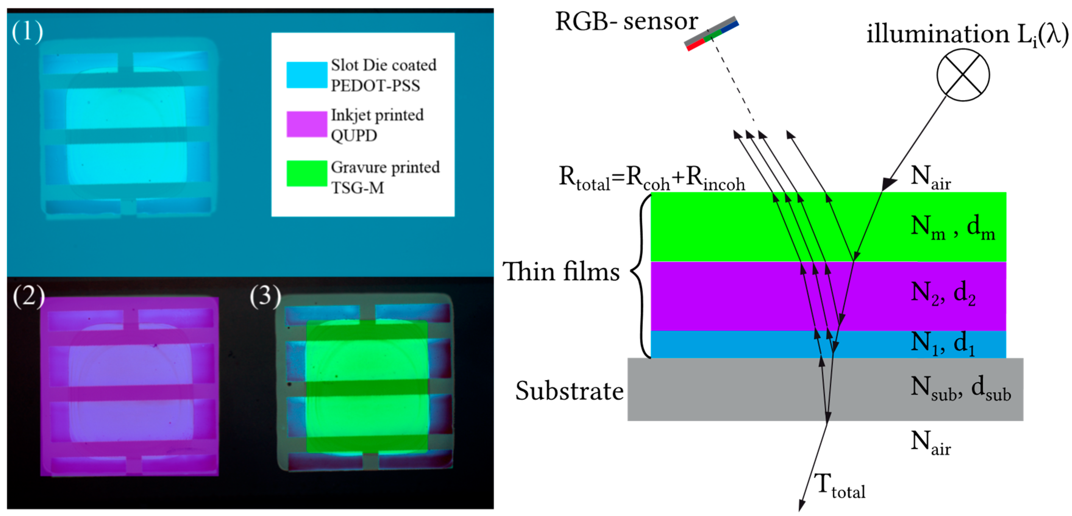
1.5. Imaging Color Reflectometry

Typical printing defects originating from hydrodynamic instabilities are in the range of several tens of micrometers up to several millimeters. In order to detect these defects, particular measurement techniques were developed in house. Imaging Color Reflectometry (ICR) uses the optical interference of thin layers with different refractive indices. By knowing the complex refractive index, it is possible to get information about the thickness of the processed films. ICR matches the experimental data to optical theory and calculates a detailed thickness map of the layer. For a detailed description of the algorithm, we refer to References [13,34,47]. This measurement technique is able to produce large area thickness mappings up to 150 mm × 100 mm. The working principle is shown in Figure 4, right. A sample with unknown thickness of the top layer is illuminated. The illumination-dependent interference is detected using a CCD- or CMOS-sensor. Using the theoretical model of the ICR method, the unknown top layer thickness can be measured. Within this work, we subsequently measured three wet-deposited layers, processed with three different high-throughput application techniques. In total, a sum of 288 different layers were measured within this work.

2. Materials and Methods

2.1. Chemicals and Materials

1-Propanol (Anhydrous, >99.7%), Toluene (Anhydrous, >99.8%), and Triton X–100 (all purchased by Sigma Aldrich, Merck KGaA, Darmstadt, Germany) were used as received. PEDOT:PSS (PVPAI 40.83 SG) was purchased from Heraeus (Leverkusen, Germany) and the cross-linkable hole transport material was provided by the COPT Center (Cologne, Germany). As an emitting material TSG-M, a green small molecule mixture was purchased from Merck KGaA (Darmstadt, Germany). Indium-tin-oxide (ITO) glass sheets with 10 ohm/sq were acquired from Kintec (Kowloon, Hong Kong).

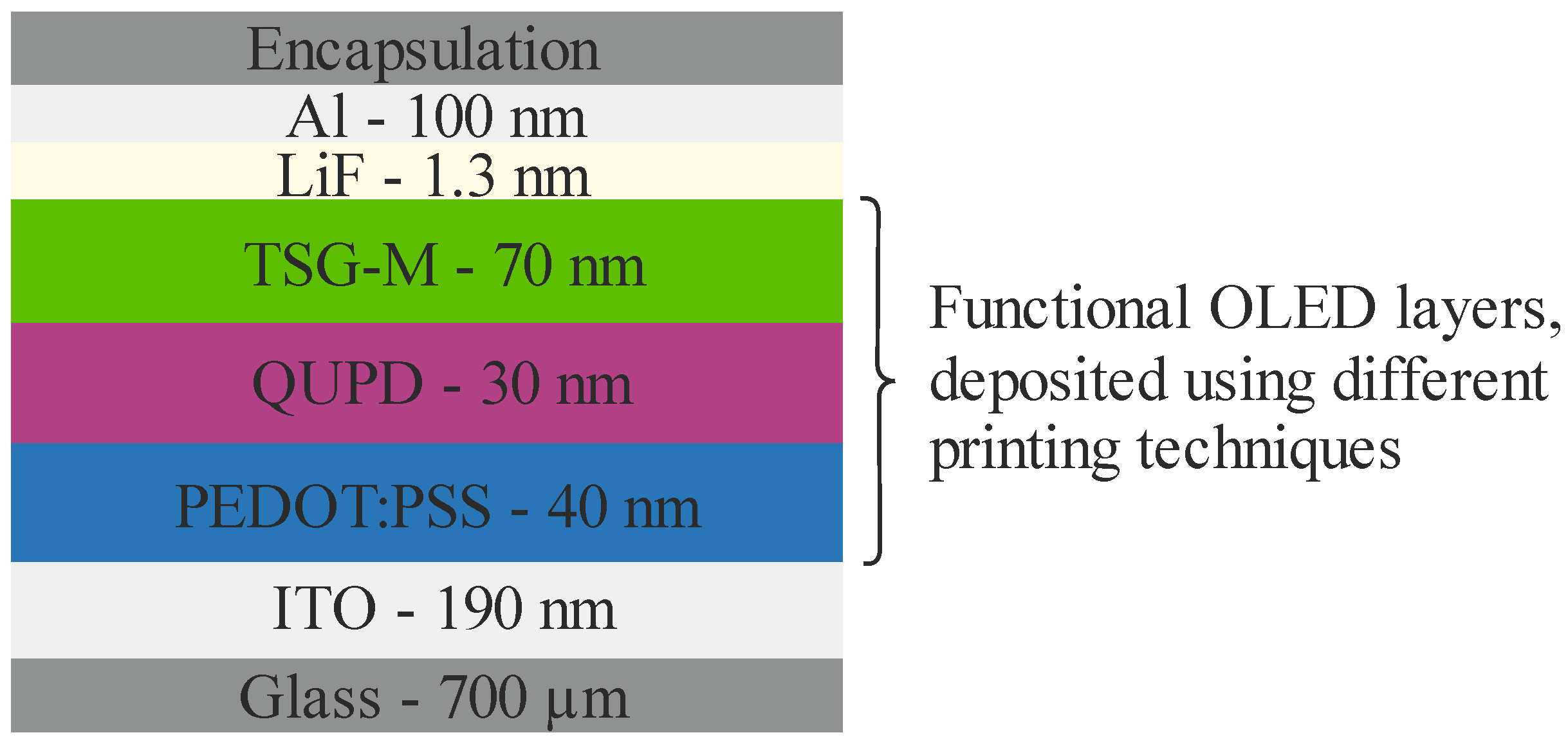
2.2. Device Fabrication

Full-area ITO glass sheets (150 × 150 mm2) were structured by applying an etching paste (Hiper-Etch purchased by Merck KGaA) via screen-printing. The OLEDs have a size of 4 × 6 mm2 as an active area. PEDOT:PSS was cast on top of the ITO by applying the deposition techniques slot die coating and inkjet printing. In order to remove aggregated PEDOT:PSS particles, the inks were filtered with a Polyvinylidene fluoride (PVDF) filter with a pore size of 0.45 µm. After coating, the PEDOT:PSS layer was thermally annealed at 200 °C for 4 min. Directly before coating the HTL, the PEDOT:PSS layers were heated up to 100 °C for 15 min to get rid of absorbed water. The detailed cross-linking steps can be seen in References [48,49]. All QUPD solutions showed strong de-wetting effects during the application on PEDOT:PSS. For a better wetting of the QUPD, the PEDOT:PSS layers were treated with Argon plasma for two minutes. For QUPD, all three application techniques were used. The different QUPD solutions as well as the TSG-M solution were filtered with a 0.2 µm Polytetrafluoroethylene (PTFE) filter. The EML of all devices under investigation was solely applied by slot die coating; therefore, the TSG-M was dissolved in toluene (30 mg mL−1). As cathodes, lithium fluoride (LiF) and aluminum (Al) were thermally evaporated at a pressure of 1.5⋅10−5 Pa. A quantity of 1.3 nm of LiF was deposited at a rate of 0.1 Å s−1 and 100 nm of Al at a rate of 3 Å s−1. After the thermal evaporation of LiF and Al, the devices were encapsulated with a glass slide and a UV glue from Delo (Windach, Germany).

2.3. Slot Die Coating

All slot die coatings were conducted with a S2S slot die table coater under ambient conditions. The setup was developed in cooperation with TSE Troller AG (Murgenthal, Switzerland). The slot die head was adjusted in the 12-o’clock position and a distance of 130 µm was set between the slot die and the substrate (Figure 1). In order to bridge the gap between the slot die and substrate with the coating solution, the syringe pump was started before the actual coating process. Subsequently, the movement of the coating table was initiated with a delay of 1700 ms and a continuous speed of 0.6 m min−1. The volume flow was adjusted to ensure a stable coating process and with respect to the desired dry layer thickness. The PEDOT:PSS ink was diluted with water and 1-Propanol. A small amount of the surfactant Triton X–100 (1 × 10⁻⁶ wt%) was added to ensure sufficient wetting on the substrate. The cross-linkable QUPD was dissolved with 2 wt% of a photo acid in toluene (15 mg mL−1).

2.4. Gravure Printing

All gravure-printed films were processed under constant process parameters using a specially design printing form. The films were prepared using a Superproofer 220 from GT+W GmbH (Rödermark, Germany), a sheet-fed laboratory scale gravure printing press. In this work, an electromechanically engraved cylinder was used. The printing speed was set to 5 m s−1 at a printing pressure of 10 N mm−1. The angle of the doctor blade was set to 70° at a printing pressure of 0.3 N mm−1. The ink was dosed directly into the gap between the doctor blade and rotating cylinder using a standard pipette. For each printing run, a total ink volume of 0.5 mL was used. This volume was sufficient to ink the whole cylinder. The used cylinder was engraved with a rectangular patch to deposit the material on the active area of the printed OLEDs. The screen ruling was 60 L cm−1 at a screen angle of 45°. The engraving angle was 130°; the tonal value was 95%. This results in a pick-up volume of approximately 8.5 mL m−2. Since all fluids were of low viscosity, independent of the solid content, the thickness of the films was adjusted by varying the concentration of the solved material. All samples were processed and dried under ambient conditions. The QUPD was dissolved with 15 mg mL−1 in a mixture of 1:1 O-xylene:indane; 2 wt% photo acid with the total weight of QUPD was added.

2.5. Inkjet Printing

The PEDOT:PSS was mixed with deionized water by volume in a 1:2 ratio. To adjust the viscosity, to adjust the wettability, and to optimize the drying process, 5 vol% glycerin and 0.01 vol% Triton X–100 were added. PEDOT:PSS was printed with a FUJIFILM Dimatix DMP2831 inkjet printing system using a 10 pl Fujifilm Dimatix cartridge (Santa Clara, CA, USA). The printhead and substrate temperature were kept at 25 °C. The best drop formation was achieved using a firing frequency of 5 kHz and a custom-designed driving waveform. The layers were printed with a drop spacing of 30 µm. The QUPD was dissolved at a concentration of 80 mg mL−1 in a binary solvent mixture of tetraline and indane mixed in a ratio of 6:4 by volume. Both QUPD and TSG-M were printed with a PIXDRO LP50 inkjet printing system using a Fujufilm Spectra S-class 80 pl print head. The best droplet formation was achieved with a print head temperature of 25 °C and a custom designed waveform. The printing speed was set to 500 mm s−1, and the substrate temperature was kept at 23 °C. The layers were printed bidirectionally with a resolution of 90 × 100 dpi and a step size of 5. Directly after the deposition, the layers were dried in a vacuum chamber at 15 mbar.

2.6. Layer and Device Characterization

To cross-check the ICR measurements, the layer thicknesses were also determined using a DEKTAK 150 tactile profilometer with a 12.5 µm tip. To perform the device measurements, the 150 × 150 mm2 substrates were cut into 25 × 25 mm2 pieces. All devices were characterized using a BOTEST measurement system (Botest Systems GmbH, Wertheim, Germany). This setup allows for the current density and luminance as a function of the applied voltage to be obtained and, therefore, allows for the device efficiency to be calculated.

3. Results

The aim of this work was to evaluate whether all three techniques are suitable for the application of certain functional OLED materials or if process limits exist for certain material/technique combinations. The focus of this study was to investigate how homogeneous and reproducible the three printing techniques can apply the different functional materials. Furthermore, OLEDs were fabricated to investigate if the combination of certain materials and printing techniques influences the device performance. In order to ensure a comparability of the OLEDs with the functional layers that were deposited using different coating techniques, both the total device thickness (the combined thickness of all functional layers) and the thickness of each functional layer should remain as constant as possible (see the Introduction Section). Therefore, for each material and coating technique, the ink formulation and process parameters were adjusted in order to obtain a functional layer with a comparable thickness. The target layer thickness of PEDOT:PSS-based HIL was 40 nm, followed by a 30 nm layer of the crosslinked hole transport material QUPD and a 70 nm thick emissive layer consisting of the TSG-M layer. The complete multilayer stack is shown in Figure 5.

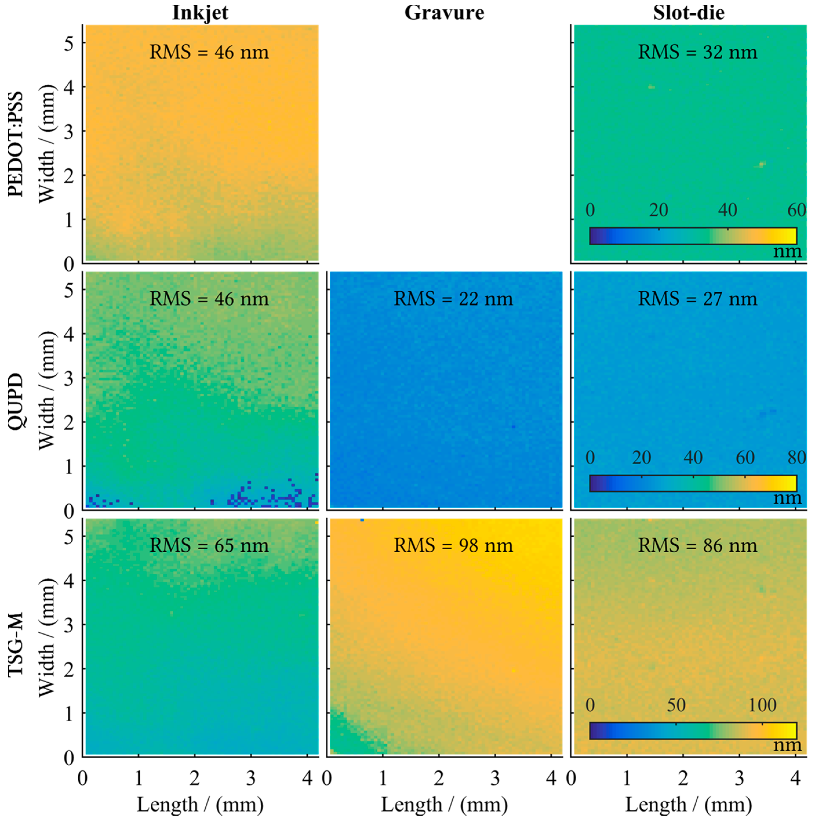
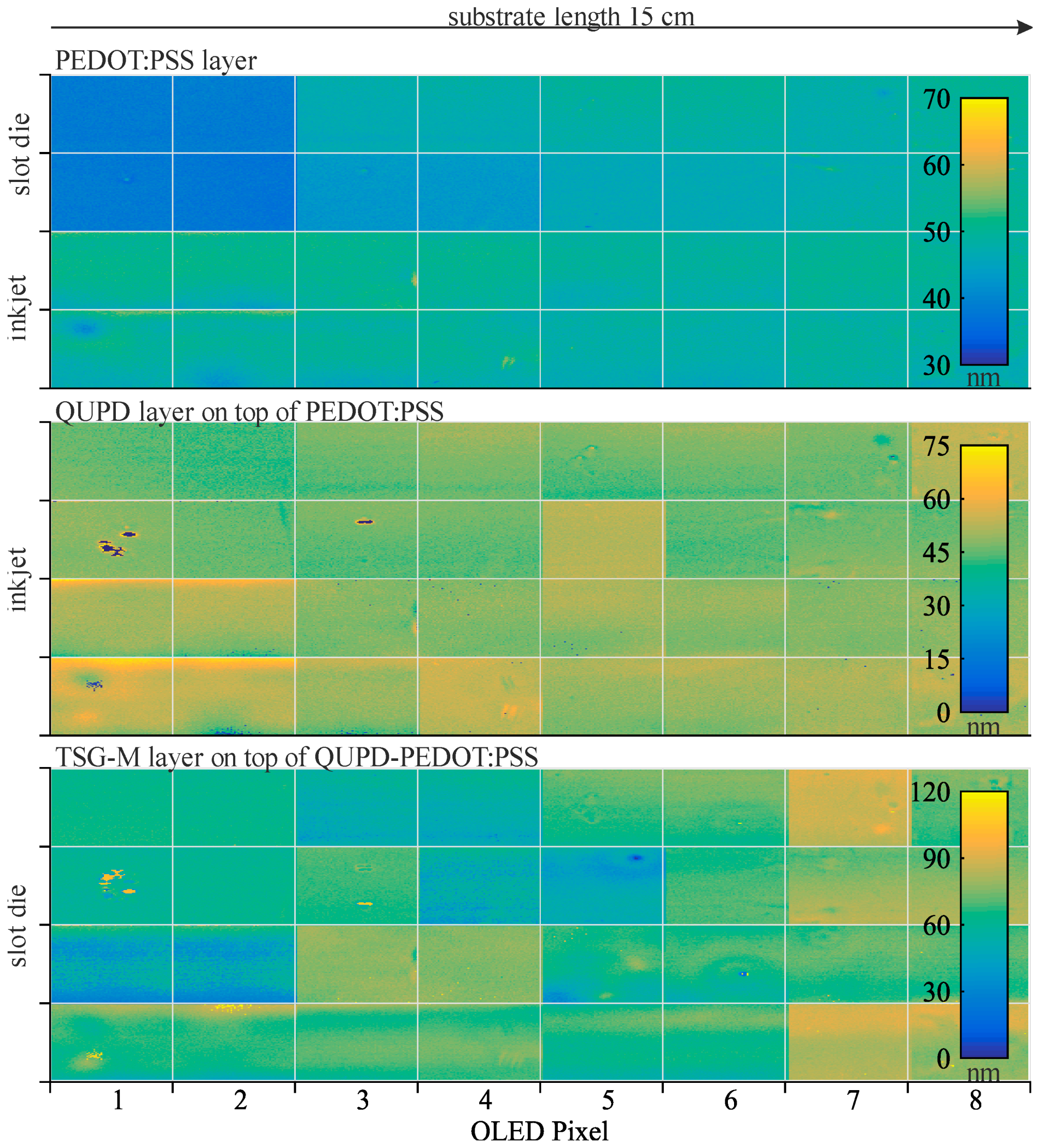
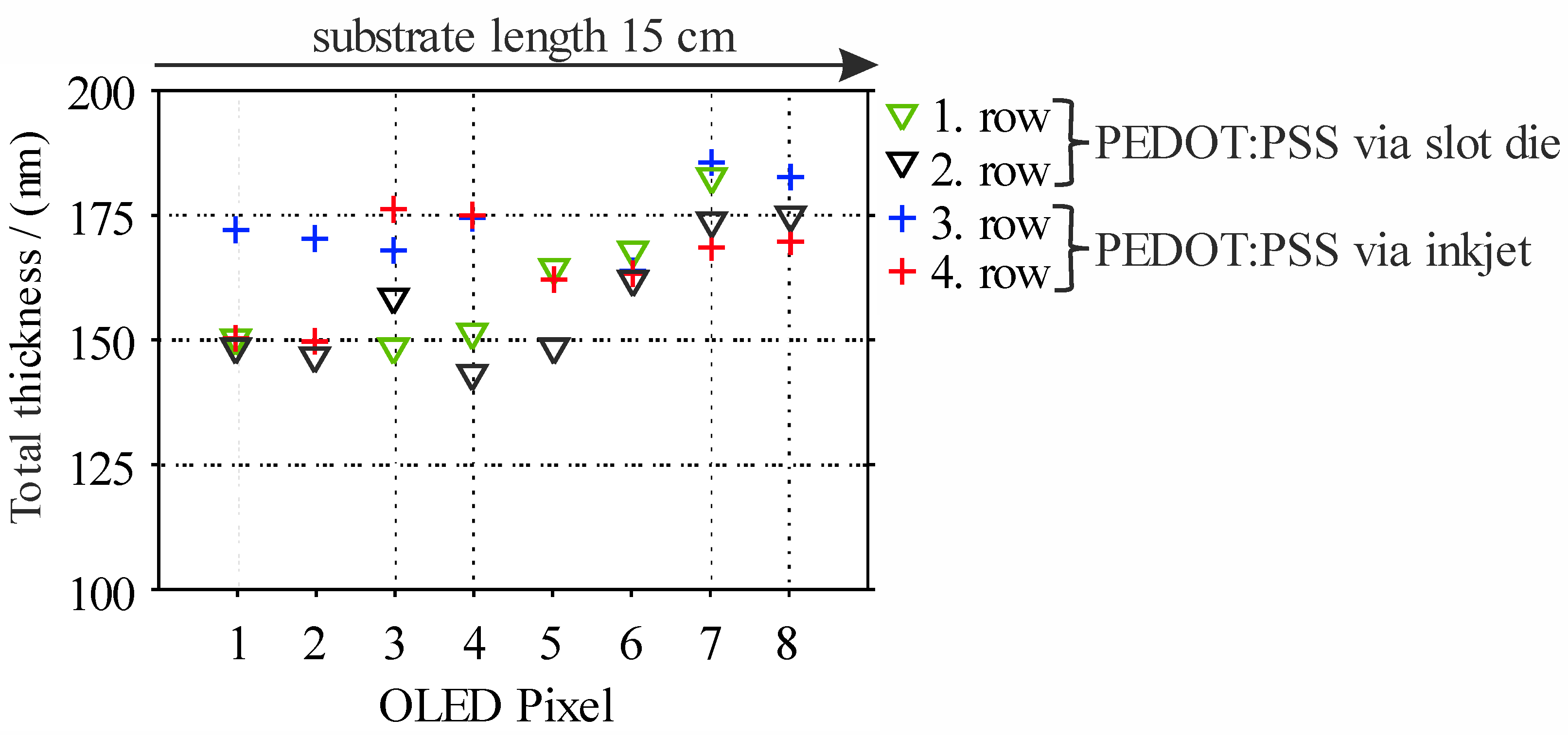
3.1. Influence of the Application Technique on Film Homogeneity

In order to evaluate the suitability of the three techniques for the application of the OLED materials, the layers were prepared with all possible material/technique combinations. The thickness and homogeneity of these layers was analyzed by ICR mappings. Tactile measurements were used to cross-check the results of the ICR measurements. The adjustment of the absolute target layer thicknesses could have been improved for each of the three techniques, but the calibration was restricted due to a limited amount of material. Therefore, it was not always possible to apply the exact amount of ink to end up with the desired dry film thickness. The ink formulations for each material had to be adjusted to meet the demands of the respective printing technique. While it was possible to formulate PEDOT:PSS inks (with additives) that were suitable for inkjet printing and slot die coating, it was not possible to find an ink composition that could be used for gravure printing. Due to agglomerate formation in the printed layer, the gravure printing of PEDOT:PSS was excluded. It can be assumed that the high shear forces at the doctor blade cause a phase separation of the multicomponent PEDOT:PSS ink. After each printing step, the top layer of the multilayer stack was measured with multichannel ICR. The resulting layer thickness mappings of the investigated material/technique combinations are displayed in Figure 6. The size of the measured area corresponds to the size of the active area of the OLEDs. As gravure printing of PEDOT:PSS was not successful; the gravure printed QUPD and TSG-M layers were applied on top of slot die coated PEDOT:PSS layers. A comparison of the QUPD layers shows that this material can be applied homogeneously with gravure printing as well as slot die coating. However, the inkjet-printed QUPD displayed a cloudy layer formation, which probably is due to the inhomogeneous drying conditions. The outliners at the lower edge are not holes in the printed layer but result from ICR evaluation artifacts. The gravure-printed and slot-die-coated layers have a comparable root mean square (RMS) value of the layer thickness, whereas the inkjet-printed QUPD with a value of 46 nm is above the targeted layer thickness of 30 nm. TSG-M could be processed with slot die coating using a toluene-based ink without any additive solvents. However, inkjet and gravure printing required longer levelling and drying times; therefore, the ink formulation was adapted by adding solvents with high boiling points like indane and tetraline. The comparison of the emissive layers shows that the TSG-M could be applied homogeneously using inkjet printing and slot die coating. The achieved layer thickness is in the range of the target layer thickness of about 70 nm, whereas the gravure-printed emissive layer exhibits a layer thickness gradient of 70 nm to 110 nm. The mappings for the different combinations of materials and techniques shown in Figure 6 are representative for the layer thicknesses of the 96 OLEDs investigated in this study. Additionally, Table 1 summarizes the suitability of the three techniques to apply the three materials homogeneously.
Since the suitability of the different scalable techniques was investigated in this study, the large-area homogeneity of the layers with the thickness in the nanometer regime is of interest on a cm-scale in the lateral direction. For this reason, the layer thickness mappings of 32 OLEDs (containing all three functional layers deposited using one of the possible material/technique combinations) are shown in Figure 7. The eight OLEDs of one row are distributed along a 15 cm long substrate. As already mentioned, the three layers were applied and measured consecutively, keeping in mind that the color mapping scales are different for the three layers, to highlight also smaller thickness variations for thinner layers, e.g., PEDOT:PSS. The first mapping of Figure 7 shows the PEDOT:PSS layer which was applied in the first two rows via slot die coating and in the two bottom rows by inkjet printing. For the slot-die-coated PEDOT:PSS layer, an increase in layer thickness in coating direction from left to right was observed. The occurrence of the layer thickness gradient during this noncontinuous coating process is due to the specific experimental setup. The second mapping shows an inkjet-printed QUPD layer, which was deposited on top of the previously shown PEDOT:PSS layer. Therefore, the shown QUPD thickness mapping was calculated from a multichannel stack measurement. The QUPD layer thicknesses of 32 pixels demonstrate good homogeneity with a layer thickness between 45–50 nm. Furthermore, these mappings visualize how printing defects propagate in the subsequently applied layers. For example, the small defects of the QUPD-layer in the second row at position 1 were detected at the same position in the TSG-M layer, which was applied on top of the QUPD layer (third mapping). The slot-die-coated TSG-M layers have thickness values in the desired range of 70 nm for all pixels. In particular, when evaluating the single layer homogeneity of the top layer of the stack—the emissive layer—it must be considered that the layer thickness measurement becomes more complex and thus more error-prone with an increasing number of underlying layers that have to be taken into account.
To compare the overall homogeneity of the individual layers, Figure 8 shows the mean total stack thickness of the 32 OLEDs displayed in Figure 7. The total stack thickness of each OLED was calculated based on the mean thickness of each of the three functional layers. The maximum total thickness deviation for all 32 pixels is limited to 30 nm. Concerning the total thickness of OLED stacks based on slot-die-coated PEDOT:PSS, two cases have to be distinguished: the standard deviation of stacks on the same position and the standard deviation of stacks on different positions. If the OLED stacks are located in the same positions, only a small standard deviation of less than 6 nm was observed. However, as the trend of a layer thickness increase could be observed for slot-die-coated PEDOT:PSS in the coating direction, the standard deviation is 9.8 nm significantly higher for the 16 OLED stacks on different positions, which are distributed on a 15 cm long substrate, but is still in the same range as the one of inkjet-printed samples (9.5 nm).

3.2. Influence of the Material/Technique Combination on OLED Performance

Despite the investigation of layer homogeneity and reproducibility, it was also investigated if the combination of certain materials and coating techniques influences the performance of OLED devices. As already mentioned, PEDOT:PSS could only be applied with slot die coating or inkjet printing, while QUPD was printed with all three techniques. Despite the coating technique that was used for the PEDOT:PSS and QUPD layer, the performance of the OLEDs with gravure and inkjet-printed TSG-M was poorer compared to the slot die coated devices. This poorer performance can be caused by different factors. It has to be considered that TSG-M ink used for slot die coating was based on pure toluene. However, the inks used for inkjet and gravure printing contained different solvents. Due to their high boiling points and low vapor pressure, these solvents can remain in the deposited layer and can also affect the morphology. Additionally, for the gravure-printed TSG-M, the pronounced thickness inhomogeneities that are shown in Figure 6 can also contribute to the poor device performance. Therefore, in the following discussion, we will focus on the device characteristics of OLEDs with a slot-die-coated EML. Using slot-die-coated TSG-M as EML six different material/technique combinations for the devices are possible (2× PEDOT:PSS/3× QUPD/1× TSG-M). The focus was to achieve reproducible layer thicknesses and reproducible OLED performances. To obtain statistically significant results, 16 OLEDs were produced for each of the six possible combinations of the materials and deposition techniques; thus, the layer thickness and device performance of 96 OLEDs was investigated in total. The criteria for the functionality of the fabricated OLEDs were oriented towards their application as light sources. Accordingly, an OLED has been considered as functional if it exceeded a minimum luminance of 1000 cd m−2 and if its IV curve had an exponential shape [1]. Only 60 of the 96 OLEDs achieved the specified requirements; the optoelectronic properties of the functional devices are summarized in Table 2. In rows 1 and 2 of Figure 7 and Figure 8, the layer thickness mappings are shown for the OLEDs SI (PEDOT:PSS applied via Slot die, QUPD applied with Inkjet). The layer thickness mappings of the OLEDs II are displayed in rows 3 and 4 (PEDOT:PSS applied via Inkjet, QUPD applied via Inkjet).
Figure 9 shows the current density–voltage and luminance–voltage characteristics of three OLEDs, which differ only in the technique with which QUPD was applied, as PEDOT:PSS and TSG-M were applied via slot die coating for all OLEDs of columns SS, SG, and SI. While QUPD for OLED column SG was applied via gravure printing, slot die coating was used for column SS and inkjet printing was used for SI. As the three selected devices achieve the average efficiency, they can be seen as a characteristic example for the respective material technique combination. The OLEDs, which the QUPD layer of was processed by slot die coating, achieved up to 30,000 cd m−2, the highest luminance, at 20 V. Furthermore, they also showed the lowest turn-on voltage of 4.3 V. However, the devices based on the inkjet-printed QUPD showed a significantly lower luminance of only 15,000 cd m−2 at 20 V and a higher turn-on voltage of 4.7 V. This might be due to the higher layer thickness and film inhomogeneities of the QUPD layer applied via inkjet printing, resulting in a higher resistance of the organic layer. The best performance in terms of efficiency with values of 13.3 cd A−1 and 2.5 lm W−1 (see Table 2 column SG) could be achieved with a combination of a slot-die-coated PEDOT:PSS and TSG-M layer, while the QUPD layer was applied via gravure printing. The efficiency of all 60 OLEDs of the different technique combinations was in a similar range from 1.3 lm W−1 to 2.5 lm W−1. Concerning the differences in device efficiency, several aspects have to be considered. The use of different application techniques led to functional layers with a slightly different thickness and different homogeneities. A change of the total device thickness or position of the recombination zone can affect the emission spectrum of the device. Furthermore, as already discussed, solvent additives used for the adaption of the ink formulation could also affect the layer morphology and device performance.

4. Discussion

In the course of this work, the suitability of the three techniques, slot die coating, inkjet printing and gravure printing, as well as combinations thereof was investigated for the application of three functional materials used for multilayer OLEDs. The three OLED materials were applied consecutively on top of the previously deposited layer. In order to compare the application techniques regarding a large area layer homogeneity (in a 150 × 100 mm2 range), the layer thicknesses were measured for each layer using Imaging Color Reflectometry (ICR). Subsequently, 96 OLEDs with three solution-processed layers were manufactured, using six different material/technique combinations, and the optoelectronic data were compared. The basic demand was the adjustment of the ink formulation towards the process-dependent requirements. This study showed that the PEDOT:PSS based hole-injection layer can only be processed using inkjet printing or slot die coating, since gravure printing was accompanied by agglomerate formation. The HTL QUPD can be applied with all three techniques. However, the best results concerning layer homogeneity could be achieved for slot die coating and gravure printing. Regarding the EML, an acceptable device performance could be only achieved by depositing TSG-M with slot die coating. The EML ink formulation led to inferior results using gravure or inkjet printing. One possible reason could be the effect of solvent additives that were required to formulate an ink that is suitable for inkjet or gravure printing. The effect of the solvent on layer morphology and device functionality has to be investigated further. The total stack thickness of 32 OLEDs could be reproduced homogeneously in a process window of 30 nm for the technique combination of slot die coating and inkjet printing. The best OLED performance in terms of efficiency with a value of 13.3 cd A−1 could be achieved with a process combination of slot die coating for PEDOT:PSS and TSG-M, while QUPD was applied using gravure printing. Of the 96 OLEDs fabricated, 60 met the criteria for functionality and achieved similar efficiency values in the range of 7.6–13.3 cd A−1 despite the different process combinations. The differences might be caused by differences in layer thickness.

Author Contributions

Conceptualization and investigation: slot die coating, L.M., M.M.; gravure printing, D.D., F.B.; inkjet printing, S.S., T.R.; material research, D.K., B.U., M.D.B.; writing—original draft preparation, L.M., D.D., F.B.; supervision and funding acquisition, K.M., G.H.-S., U.L., H.M.S., E.D., P.S., W.S.

Funding

This research was funded by Federal Ministry of Education and Research via the project POESIE (contract number 13N13692).

Acknowledgments

We would like to thank all mechanics, assistants, and students involved for contributing to this work, as well as TSE Troller AG, Murgenthal, Switzerland and GT+W GmbH, Rödermark for the technical support. We thank Alexander Jurczok from IDD, Technische Universität Darmstadt for structuring the ITO substrates. The authors are also thankful for the support of Innovation Lab GmbH, Heidelberg, Germany.

Conflicts of Interest

The authors declare no conflict of interest.

References

  1. OE-A VDMA. The German Engineering Federation, 7th ed.; OE-A Roadmap: Washington, DC, USA, 2017. [Google Scholar]
  2. Duggal, A.R.; Heller, C.M.; Shiang, J.J.; Liu, J.; Lewis, L.N. Solution-Processed Organic Light-Emitting Diodes for Lighting. J. Display Technol. 2007, 3, 184–192. [Google Scholar] [CrossRef]
  3. Aizawa, N.; Pu, Y.-J.; Watanabe, M.; Chiba, T.; Ideta, K.; Toyota, N.; Igarashi, M.; Suzuri, Y.; Sasabe, H.; Kido, J. Solution-processed multilayer small-molecule light-emitting devices with high-efficiency white-light emission. Nat. Commun. 2014, 5, 5756. [Google Scholar] [CrossRef] [PubMed] [Green Version]
  4. Park, B.; Kwon, O.E.; Yun, S.H.; Jeon, H.G.; Huh, Y.H. Organic semiconducting layers fabricated by self-metered slot-die coating for solution-processable organic light-emitting devices. J. Mater. Chem. C 2014, 2, 8614–8621. [Google Scholar] [CrossRef]
  5. Chang, H.-W.; Lee, Y.-T.; Tseng, M.-R.; Jang, M.-H.; Yeh, H.-C.; Luo, F.-T.; Meng, H.-F.; Chen, C.-T.; Chi, Y.; Qiu, Y.; et al. General application of blade coating to small-molecule hosts for organic light-emitting diode. Synth. Met. 2014, 196, 99–109. [Google Scholar] [CrossRef]
  6. Søndergaard, R.R.; Hösel, M.; Krebs, F.C. Roll-to-Roll fabrication of large area functional organic materials. J. Polym. Sci. B Polym. Phys. 2013, 51, 16–34. [Google Scholar] [CrossRef]
  7. Krebs, F.C. Fabrication and processing of polymer solar cells: A review of printing and coating techniques. Solar Energy Mater. Solar Cells 2009, 93, 394–412. [Google Scholar] [CrossRef]
  8. Gather, M.C.; Kronenberg, N.M.; Meerholz, K. Monolithic integration of multi-color organic LEDs by grayscale lithography. Adv. Mater. 2010, 22, 4634–4638. [Google Scholar] [CrossRef] [PubMed]
  9. Chung, D.-Y.; Huang, J.; Bradley, D.D.C.; Campbell, A.J. High performance, flexible polymer light-emitting diodes (PLEDs) with gravure contact printed hole injection and light emitting layers. Org. Electron. 2010, 11, 1088–1095. [Google Scholar] [CrossRef]
  10. Hegemann, D.; Brunner, H.; Oehr, C. Plasma treatment of polymers for surface and adhesion improvement. Nucl. Instrum. Methods Phys. Res. Sect. B Beam Int. Mater. Atoms 2003, 208, 281–286. [Google Scholar] [CrossRef]
  11. Kim, S.R. Surface modification of poly(tetrafluoroethylene) film by chemical etching, plasma, and ion beam treatments. J. Appl. Polym. Sci. 2000, 77, 1913–1920. [Google Scholar] [CrossRef]
  12. Choi, K.-J.; Lee, J.-Y.; Park, J.; Seo, Y.-S. Multilayer slot-die coating of large-area organic light-emitting diodes. Org. Electron. 2015, 26, 66–74. [Google Scholar] [CrossRef]
  13. Raupp, S.; Daume, D.; Tekoglu, S.; Merklein, L.; Lemmer, U.; Hernandez-Sosa, G.; Sauer, H.M.; Dörsam, E.; Scharfer, P.; Schabel, W. Slot Die Coated and Flexo Printed Highly Efficient SMOLEDs. Adv. Mater. Technol. 2016, 2, 1600230. [Google Scholar] [CrossRef]
  14. Duan, L.; Hou, L.; Lee, T.-W.; Qiao, J.; Zhang, D.; Dong, G.; Wang, L.; Qiu, Y. Solution processable small molecules for organic light-emitting diodes. J. Mater. Chem. 2010, 20, 6392–6407. [Google Scholar] [CrossRef] [Green Version]
  15. Choi, K.-J.; Lee, J.-Y.; Shin, D.-K.; Park, J. Investigation on slot-die coating of hybrid material structure for OLED lightings. J. Phys. Chem. Solids 2016, 95, 119–128. [Google Scholar] [CrossRef]
  16. Elschner, A.; Heuer, H.W.; Jonas, F.; Kirchmeyer, S.; Wehrmann, R.; Wussow, K. Gallium Complexes in Three-Layer Organic Electroluminescent Devices. Adv. Mater. 2001, 13, 1811–1814. [Google Scholar] [CrossRef]
  17. Abbel, R.; de Vries, I.; Langen, A.; Kirchner, G.; t’Mannetje, H.; Gorter, H.; Wilson, J.; Groen, P. Toward high volume solution based roll-to-roll processing of OLEDs. J. Mater. Res. 2017, 32, 2219–2229. [Google Scholar] [CrossRef] [Green Version]
  18. Tekoglu, S.; Hernandez-Sosa, G.; Kluge, E.; Lemmer, U.; Mechau, N. Gravure printed flexible small-molecule organic light emitting diodes. Org. Electron. 2013, 14, 3493–3499. [Google Scholar] [CrossRef]
  19. Olivier, S.; Ishow, E.; Della-Gatta, S.M.; Maindron, T. Inkjet deposition of a hole-transporting small molecule to realize a hybrid solution-evaporation green top-emitting OLED. Org. Electron. 2017, 49, 24–32. [Google Scholar] [CrossRef]
  20. Zhou, L.; Yang, L.; Yu, M.; Jiang, Y.; Liu, C.-F.; Lai, W.-Y.; Huang, W. Inkjet-Printed Small-Molecule Organic Light-Emitting Diodes: Halogen-Free Inks, Printing Optimization, and Large-Area Patterning. ACS Appl. Mater. Interfaces 2017, 9, 40533–40540. [Google Scholar] [CrossRef] [PubMed]
  21. Stolz, S.; Scherer, M.; Mankel, E.; Lovrinčić, R.; Schinke, J.; Kowalsky, W.; Jaegermann, W.; Lemmer, U.; Mechau, N.; Hernandez-Sosa, G. Investigation of solution-processed ultrathin electron injection layers for organic light-emitting diodes. ACS Appl. Mater. Interfaces 2014, 6, 6616–6622. [Google Scholar] [CrossRef] [PubMed]
  22. Verma, A.; Zink, D.M.; Fléchon, C.; Leganés Carballo, J.; Flügge, H.; Navarro, J.M.; Baumann, T.; Volz, D. Efficient, inkjet-printed TADF-OLEDs with an ultra-soluble NHetPHOS complex. Appl. Phys. A 2016, 122, 191. [Google Scholar] [CrossRef]
  23. Schmitt, M.; Scharfer, P.; Schabel, W. Slot die coating of lithium-ion battery electrodes: Investigations on edge effect issues for stripe and pattern coatings. J. Coat. Technol. Res. 2014, 11, 57–63. [Google Scholar] [CrossRef]
  24. Peters, K.; Wengeler, L.; Scharfer, P.; Schabel, W. Liquid film coating of small molecule OLEDs. J. Coat. Technol. Res. 2014, 11, 75–81. [Google Scholar] [CrossRef]
  25. Raupp, S.M.; Schmitt, M.; Walz, A.-L.; Diehm, R.; Hummel, H.; Scharfer, P.; Schabel, W. Slot die stripe coating of low viscous fluids. J. Coat. Technol. Res. 2018, 30, 363. [Google Scholar] [CrossRef]
  26. Schmitt, M.; Diehm, R.; Scharfer, P.; Schabel, W. An experimental and analytical study on intermittent slot die coating of viscoelastic battery slurries. J. Coat. Technol. Res. 2015, 12, 927–938. [Google Scholar] [CrossRef]
  27. Buerkin, C.K.; de Vries, I.; Raupp, S.M.; Scharfer, P.; Schabel, W.; Groen, P. Investigation of interfacial instabilities with a two-layer slide coating process. J. Coat. Technol. Res. 2017, 14, 991–1001. [Google Scholar] [CrossRef]
  28. Horiuchi, R.; Suszynski, W.J.; Carvalho, M.S. Simultaneous multilayer coating of water-based and alcohol-based solutions. J. Coat. Technol. Res. 2015, 12, 819–826. [Google Scholar] [CrossRef]
  29. Kistler, S.F.; Schweizer, P.M. Liquid Film Coating: Scientific Principles and Their Technological Implications; Chapman & Hall: London, UK, 1997. [Google Scholar]
  30. Gutoff, E.B.; Cohen, E.D.; Kheboian, G.I. Coating and Drying Defects: Troubleshooting Operating Problems, 2nd ed.; Wiley-Interscience: Hoboken, NJ, USA, 2006. [Google Scholar]
  31. Raupp, S.M.; Merklein, L.; Pathak, M.; Scharfer, P.; Schabel, W. An experimental study on the reproducibility of different multilayer OLED materials processed by slot die coating. Chem. Eng. Sci. 2017, 160, 113–120. [Google Scholar] [CrossRef]
  32. Raupp, S.M.; Merklein, L.; Hietzschold, S.; Zürn, M.; Scharfer, P.; Schabel, W. Slot die-coated blue SMOLED multilayers. J. Coat. Technol. Res. 2017, 10, 1029–1037. [Google Scholar] [CrossRef]
  33. Nisato, G.; Donald, L.; Simone, G. Organic and Printed Electronics: Fundamentals and Applications; CRC Press: Boca Raton, FL, USA, 2016. [Google Scholar]
  34. Bornemann, N. Characterization and Investigation of Large-Area, Ultra-Thin Gravure Printed Layers. Ph.D. Thesis, Technische Universität Darmstadt, Darmstadt, Germany, May 2014. [Google Scholar]
  35. Fields, R.J.; Ashby, M.F. Finger-like crack growth in solids and liquids. Philos. Mag. 1976, 33, 33–48. [Google Scholar] [CrossRef]
  36. Gingras, M.J.P.; Rácz, Z. Noise and the linear stability analysis of viscous fingering. Phys. Rev. A 1989, 40, 5960–5965. [Google Scholar] [CrossRef]
  37. Ben Amar, M. Viscous fingering in a wedge. Phys. Rev. A 1991, 44, 3673–3685. [Google Scholar] [CrossRef] [PubMed]
  38. Derby, B. Inkjet Printing of Functional and Structural Materials: Fluid Property Requirements, Feature Stability, and Resolution. Annu. Rev. Mater. Res. 2010, 40, 395–414. [Google Scholar] [CrossRef]
  39. Cummins, G.; Desmulliez, M.P.Y. Inkjet printing of conductive materials: A review. Circuit World 2012, 38, 193–213. [Google Scholar] [CrossRef]
  40. Eggenhuisen, T.M.; Galagan, Y.; Biezemans, A.F.K.V.; Slaats, T.M.W.L.; Voorthuijzen, W.P.; Kommeren, S.; Shanmugam, S.; Teunissen, J.P.; Hadipour, A.; Verhees, W.J.H.; et al. High efficiency, fully inkjet printed organic solar cells with freedom of design. J. Mater. Chem. A 2015, 3, 7255–7262. [Google Scholar] [CrossRef] [Green Version]
  41. Coenen, M.J.J.; Slaats, T.M.W.L.; Eggenhuisen, T.M.; Groen, P. Inkjet printing the three organic functional layers of two-colored organic light emitting diodes. Thin Solid Films 2015, 583, 194–200. [Google Scholar] [CrossRef]
  42. Morfa, A.J.; Rödlmeier, T.; Jürgensen, N.; Stolz, S.; Hernandez-Sosa, G. Comparison of biodegradable substrates for printed organic electronic devices. Cellulose 2016, 23, 3809–3817. [Google Scholar] [CrossRef]
  43. Inzelberg, L.; Pur, M.D.; Schlisske, S.; Rödlmeier, T.; Granoviter, O.; Rand, D.; Steinberg, S.; Hernandez-Sosa, G.; Hanein, Y. Printed facial skin electrodes as sensors of emotional affect. Flex. Print. Electron. 2018, 3, 045001. [Google Scholar] [CrossRef]
  44. Gao, M.; Li, L.; Song, Y. Inkjet printing wearable electronic devices. J. Mater. Chem. C 2017, 5, 2971–2993. [Google Scholar] [CrossRef]
  45. De Gans, B.-J.; Schubert, U.S. Inkjet printing of well-defined polymer dots and arrays. Langmuir ACS J. Surf. Colloids 2004, 20, 7789–7793. [Google Scholar] [CrossRef] [PubMed]
  46. Soltman, D.; Subramanian, V. Inkjet-printed line morphologies and temperature control of the coffee ring effect. Langmuir ACS J. Surf. Colloids 2008, 24, 2224–2231. [Google Scholar] [CrossRef] [PubMed]
  47. Bornemann, N.; Sauer, H.M.; Dörsam, E. Gravure Printed Ultrathin Layers of Small-Molecule Semiconductors on Glass. J. Imaging Sci. Technol. 2011, 55, 40201. [Google Scholar] [CrossRef]
  48. Rehmann, N.; Hertel, D.; Meerholz, K.; Becker, H.; Heun, S. Highly efficient solution-processed phosphorescent multilayer organic light-emitting diodes based on small-molecule hosts. Appl. Phys. Lett. 2007, 91, 103507. [Google Scholar] [CrossRef]
  49. Bayerl, M.S.; Braig, T.; Nuyken, O.; Müller, D.C.; Groß, M.; Meerholz, K. Crosslinkable hole-transport materials for preparation of multilayer organic light emitting devices by spin-coating. Macromol. Rapid Commun. 1999, 20, 224–228. [Google Scholar] [CrossRef]
Figure 1. (A) The schematic process flow for slot die coating of the N,N′-bis(4-(6-((3-ethyloxetan-3-yl)methoxy)-hexyloxy)phenyl)-N,N′-bis(4-methoxyphenyl)biphenyl-4,4′-diamin (QUPD) ink on top of poly(3,4-ethylenedioxythiophene)-poly(styrenesulfonate) (PEDOT:PSS) and (B) an image of the used sheet-to-sheet (S2S) table coater.
Colloids 03 00032 g001
Figure 2. (A) A scheme of the used shuttle-based gravure printing process: The shuttle is moving from the right to the left side, whereas the printing cylinder is rotating counterclockwise. The fluid is dosed directly into the nip between the doctor blade and the gravure cylinder. (B) A picture of the used printing press Superproofer 220 produced by GT+W GmbH.
Colloids 03 00032 g002
Figure 3. (A) A scheme of the inkjet printing process: The printhead is moving over the substrate while depositing single drops in the printing direction. (B) An image of the used PixDro LP50 laboratory inkjet printer produced by Meyer Burger.
Colloids 03 00032 g003
Figure 4. Left: An overview of the different layers fabricated by different techniques and the sizes of the applied layers: The blue layer indicates PEDOT:PSS applied by slot die coating. (1) It can be seen that this technique is non-structuring. (2) The inkjet-printed layer covers the whole device shown by the purple field. (3) The TSG-M is gravure printed and covers just the desired active area of the OLED pixels, pointed out by the green area. Right: The working principle of Imaging Color Reflectometry: The thin film stack is illuminated with a light source. The interference of this stack is detected by an RGB detector. With a known refractive index and the theoretical model of the Imaging Color Reflectometry, the thickness of the top layer can be calculated.
Colloids 03 00032 g004
Figure 5. The investigated multilayer stack consisting of three subsequently solution-processed functional layers.
Colloids 03 00032 g005
Figure 6. The layer thickness mappings of the eight possible material/technique combinations: The color bar shows the layer thickness in nanometers for each layer. The root mean square of the layer thickness (RMS) value of the layer thickness is given for all mappings.
Colloids 03 00032 g006
Figure 7. The thickness mappings of 32 different OLED pixels fabricated on a 15 cm long substrate: Each mapping shows all measured pixels of the same substrate after every printing step. From top to bottom, the thickness mappings of PEDOT:PSS, QUPD (on top of PEDOT:PSS), and TSG-M (on top of QUPD/PEDOT:PSS) are shown. The first two rows of the PEDOT:PSS mapping were processed via slot die coating; the two bottom rows were applied using inkjet printing. The complete QUPD was inkjet-printed, and the complete TSG-M was slot-die-coated. Every OLED pixel has a size of 6 mm × 4 mm.
Colloids 03 00032 g007
Figure 8. The total thickness of the 32 OLEDs displayed in Figure 7 versus their position on a 15 cm long substrate: The total thicknesses were calculated based on the sum of the thicknesses of the three functional layers measured with Imaging Color Reflectometry (ICR). Every shown point represents the averaged layer thickness of the active area of one pixel. The stacks based on the PEDOT:PSS that was slot-die-coated are marked with triangles, while the ones based on inkjet-printed PEDOT:PSS are marked with crosses.
Colloids 03 00032 g008
Figure 9. The current density (black) and luminance (blue) versus the applied voltage of three OLEDs achieved the average power efficiency for the respective process combinations. For all three OLEDs, PEDOT:PSS and TSG-M were processed using slot die coating. QUPD was applied for column SG by gravure printing, for column SS by slot die coating, and for column SI via inkjet printing. The inset shows a working OLED with an active area of 24 mm2.
Colloids 03 00032 g009
Table 1. An overview of the investigated technique/material combinations, including the evaluation of the applied layers: If the material could be applied homogeneously with the corresponding technique, it is marked with a check. The combination inkjet/TSG-M is marked with a check in brackets, since inkjet can be used to apply homogeneous TSG-M layers, but the fabricated devices were almost nonfunctional (see Section 3.2.).
InkjetGravureSlot Die
PEDOT:PSSagglomerate formation
QUPDcloudy layer
TSG-M(✓)thickness gradient
Table 2. The LIV characteristics of OLED devices consisting of three solution-processed layers (active area of 24 mm2), processed using different application techniques. For each substrate, it is stated which application technique was used to apply the respective layers. SD stands for slot die coating, IJ stands for inkjet, and GP stands for gravure printing. The averaged current efficiency and power efficiency are shown for each row including standard deviation.
Technique CombinationSSISSGIGSIII
PEDOT:PSSSDIJSDIJSDIJ
QUPDSDSDGPGPIJIJ
TSG-MSDSDSDSDSDSD
Yield9/1613/1610/1611/126/1611/16
Current effic. (cd A−1)10.9 ± 0.99.7 ± 0.912.9 ± 0.48.4 ± 0.810.6 ± 1.19.0 ± 0.9
Power effic. (lm W−1)2.2 ± 0.11.7 ± 0.22.4 ± 0.11.4 ± 0.12.0 ± 0.11.7 ± 0.2
Voltage at 1000 cd m−211.3 ± 0.812.0 ± 0.812.7 ± 0.613.6 ± 0.411.3 ± 0.710.5 ± 0.8

