Article

The Effect of Doping with Aluminum on the Optical, Structural, and Morphological Properties of Thin Films of SnO2 Semiconductors

by
Isis Chetzyl Ballardo Rodriguez
1,
U. Garduño Terán
2,
A. I. Díaz Cano
2,
B. El Filali
1,* and
M. Badaoui
3
1
Instituto Politécnico Nacional, UPIITA, México City 07340, Mexico
2
Instituto Politécnico Nacional, SEPI-UPIITA, México City 07340, Mexico
3
Instituto Politécnico Nacional, Escuela Superior de Ingeniería Mecánica y Eléctrica, México City 07738, Mexico
*
Author to whom correspondence should be addressed.
J. Compos. Sci. 2025, 9(7), 358; https://doi.org/10.3390/jcs9070358
Submission received: 30 May 2025 / Revised: 28 June 2025 / Accepted: 3 July 2025 / Published: 9 July 2025
(This article belongs to the Special Issue Optical–Electric–Magnetic Multifunctional Composite Materials)

Abstract

There is considerable interest in broadband nanomaterials, particularly transparent semiconductor oxides, within both fundamental research and technological applications. Historically, it has been considered that the variation in dopant concentration during the synthesis of semiconductor materials is a crucial factor in activating and/or modulating the optical and structural properties, particularly the bandgap and the parameters of the unit cell, of semiconductor oxides. Recently, tin oxide has emerged as a key material due to its excellent structural properties, optical transparency, and various promising applications in optoelectronics. This study utilized the ultrasonic spray pyrolysis technique to synthesize aluminum-doped tin oxide (ATO) thin films on quartz and polished single-crystal silicon substrates. The impact of varying aluminum doping levels (0, 2, 5, and 10 at. %) on morphology and structural and optical properties was examined. The ATO thin films were characterized using scanning electron microscopy (SEM), X-ray diffraction (XRD), and transmittance spectroscopy. SEM images demonstrated a slight reduction in the size of ATO nanoparticles as the aluminum doping concentration increased. XRD analysis revealed a tetragonal crystalline structure with the space group P42/mnm, and a shift in the XRD peaks to higher angles was noted with increasing aluminum content, indicating a decrease in the crystalline lattice parameters of ATO. The transmittance of the ATO films varied between 75% and 85%. By employing the transmittance spectra and the established Tauc formula the optical bandgap values of ATO films were calculated, showing an increase in the bandgap with higher doping levels. These findings were thoroughly analyzed and discussed; additionally, an effort was made to clarify the contradictory analyses present in the literature and to identify a doping range that avoids the onset of a secondary phase.

1. Introduction

Traditionally, it has been understood that variations in dopant concentration during the synthesis of semiconductor materials are crucial for altering their optical and structural characteristics, particularly the bandgap and the unit cell parameters. Nanomaterials based on transparent conducting oxides (TCOs), such as zinc oxide (ZnO), indium tin oxide (ITO), and tin oxide (SnO2) thin films, have gained significant interest in recent years. This interest is mainly because these semiconductors offer good electrical conductivity along with high optical transparency in the visible spectrum range (400–800 nm) and have a low production cost and minimal toxicity [1,2,3,4]. These properties are fundamental in emerging technological applications, including gas sensors, flat panel displays, solar cells, LED technology, and aircraft windshield manufacture [5,6,7].
In this context, SnO2 has gained popularity as an intrinsic n-type semiconductor [8] as it exhibits notable thermal and chemical stability under normal ambient conditions, in addition to its non-stoichiometric nature [9,10]. This semiconductor material exhibits a tetragonal rutile-type crystal structure, with space group P42/mnm, and has a direct bandgap of 3.6 eV at 300 K. Recently, prior investigations have proven that the performance of the semiconductor SnO2 is optimized when used in small metal-doped nanostructures. Various SnO2 nanostructures doped with magnetic, transition, and rare earth metals have been successfully developed, particularly in the form of thin films or nanoparticles, which has allowed for an improvement in the properties of SnO2, for example, for its use in gas detection sensors [9,10].
Currently, several techniques are available for synthesizing pure and doped tin oxide thin films. Among the most well-known techniques are magnetron sputtering [11,12], molecular beam epitaxy (MBE) [13], pulsed laser deposition (PLD) [14], chemical vapor deposition (CVD) [15], atomic layer deposition (ALD) [16], and spray pyrolysis [9,17]. The latter stands out as the most versatile and lowest cost technique for obtaining semiconductor thin films as it allows for the precise control of deposition parameters with reproducible results and can be scaled to electronic devices that cover large areas [18,19,20].
Nevertheless, tin oxide has shown stability challenges in reducing environments (such as oxidizing environments with high relative humidity), primarily due to the excessive formation of charge carriers linked to oxygen vacancies. Therefore, it is essential to introduce a dopant that can enhance the stability of the tin oxide semiconductor [21,22]. Doping SnO2 with aluminum presents a promising solution as it has demonstrated the ability to improve stability in reducing atmospheres. Additionally, aluminum is abundantly available in nature and possesses low toxicity concerns [23,24]. Consequently, Al-doped SnO2 (ATO) has gained significant interest across various technological domains, being recognized as an outstanding material for applications in perovskite solar cells, smart displays, thin-film transistors (TFTs), lithium-ion batteries, dye-sensitized solar cells (DSSCs), and the development of nanomaterials for environmental pollution control [22,23,24,25,26,27,28]. Previous research has shown that the bandgap material generally decreases as the concentration of Al dopants increases [29,30,31]. Other studies have indicated that the bandgap, nanoparticle size, and lattice parameters remain nearly unchanged despite variations in the doping level with aluminum impurities [32]. Conversely, other research indicates that the bandgap may increase with higher Al dopant levels, as shown in [33,34]. Investigations have revealed variations in both lattice parameters and nanoparticle size, corresponding to changes in the percentage of aluminum content. Upon reviewing the literature, various articles can be identified that exemplify the points discussed earlier in this research. In [35], thin films of ATO (with doping levels ranging from 0% to 5%) were synthesized for use as sensors in hydrogen detection. The authors reported that the optimal response of the hydrogen sensor based on ATO material was achieved at an aluminum doping level of 3%. Additionally, they initially observed a decrease in the grain size, the average roughness, and the unit cell parameters a and c. Subsequently, an increase in the bandgap was noted with higher doping levels of aluminum ions.
The recently published [20] describes the production of thin films of aluminum-doped tin oxide, with doping levels ranging from 0% to 4%, using the sol–gel method via spin coating. The authors present SEM image analysis indicating that the average size of the nanoparticles is approximately 1 μm. In the XRD analysis, the unit cell parameters were calculated, reporting that these increase with higher doping levels while the size of the nanoparticles in the Miller plane (110) decreases. Using the Tauc formula, the bandgap values were determined, finding that these decrease as the concentration of Al ions in the samples increases.
Despite significant research documented on ATO, more comprehensive studies are needed on this highly promising material, particularly in the field of physical chemistry, with a focus on point defects and their impact on optoelectronic properties. Additionally, it is important to note that several relevant optoelectronic or structural parameters, such as the bandgap and unit cell parameters of ATO, have been inadequately determined or have not been thoroughly explored in a clear and precise manner. At the same time, limited attention has been given to analyzing results obtained from SEM, XRD, and transmittance [24].
This article aims to resolve the conflicting analyses found in the literature, as well as to determine a doping range that avoids the formation of a secondary phase. Furthermore, we will examine the impact of incorporating Al ions into the unit cell of the ATO samples on their optical, structural, and morphological properties.

2. Materials and Methods

Tin chloride dihydrate (SnCl4 · 2H2O) was used as a tin source to prepare the main solution, while aluminum chloride (AlCl3 · 6H2O) was used as the source of the aluminum dopant.
Both solutions were prepared at a molarity of 0.05 M, using a 1:1 ratio of double-distilled water and methanol. The solutions were maintained under constant stirring to ensure adequate homogeneity. To stabilize the solutions, 2% hydrochloric acid was added, resulting in clear, precipitate-free solutions with a measured pH of 1. The solutions were then combined in specific proportions to achieve aluminum percentages of 0.0, 2.0, 5.0, and 10.0 atomic percent (at. %).
The silicon and quartz substrates, which had been previously cleaned with nitric acid, acetone, methanol, and distilled water, were dried using a nitrogen flow. The prepared solution was deposited onto the substrates through ultrasonic spray pyrolysis at a temperature of 400 °C for 30 min, utilizing a nitrogen flow of 5 L/min. After synthesizing the ATO thin films, they were annealed at 450 °C for 2 h.
A scanning electron microscope (SEM), model JSM7800F-JEOL (3-1-2 Musashino, Akishima, Tokyo 196-8558, Japan), was employed to capture images of the ATO thin film surfaces, The SEM featured an Apollo X10 EDAX detector for estimating chemical compositions using energy dispersive spectroscopy (EDS). X-ray diffraction (XRD) patterns were recorded using an X’ Pert MRD diffractometer (Enigma Business Park, Grovewood Road, Malvern, WR14 1XZ, United Kingdom), equipped with a Cu X-ray source (Kα1 = 1.5406 Å). Transmittance measurements were performed using an Ocean Optics USB2000 UV-VIS spectrometer (3500 Quadrangle Blvd, Orlando, FL, USA) fitted with a DT 1000 CE US.VIS lamp.

3. Results and Discussion

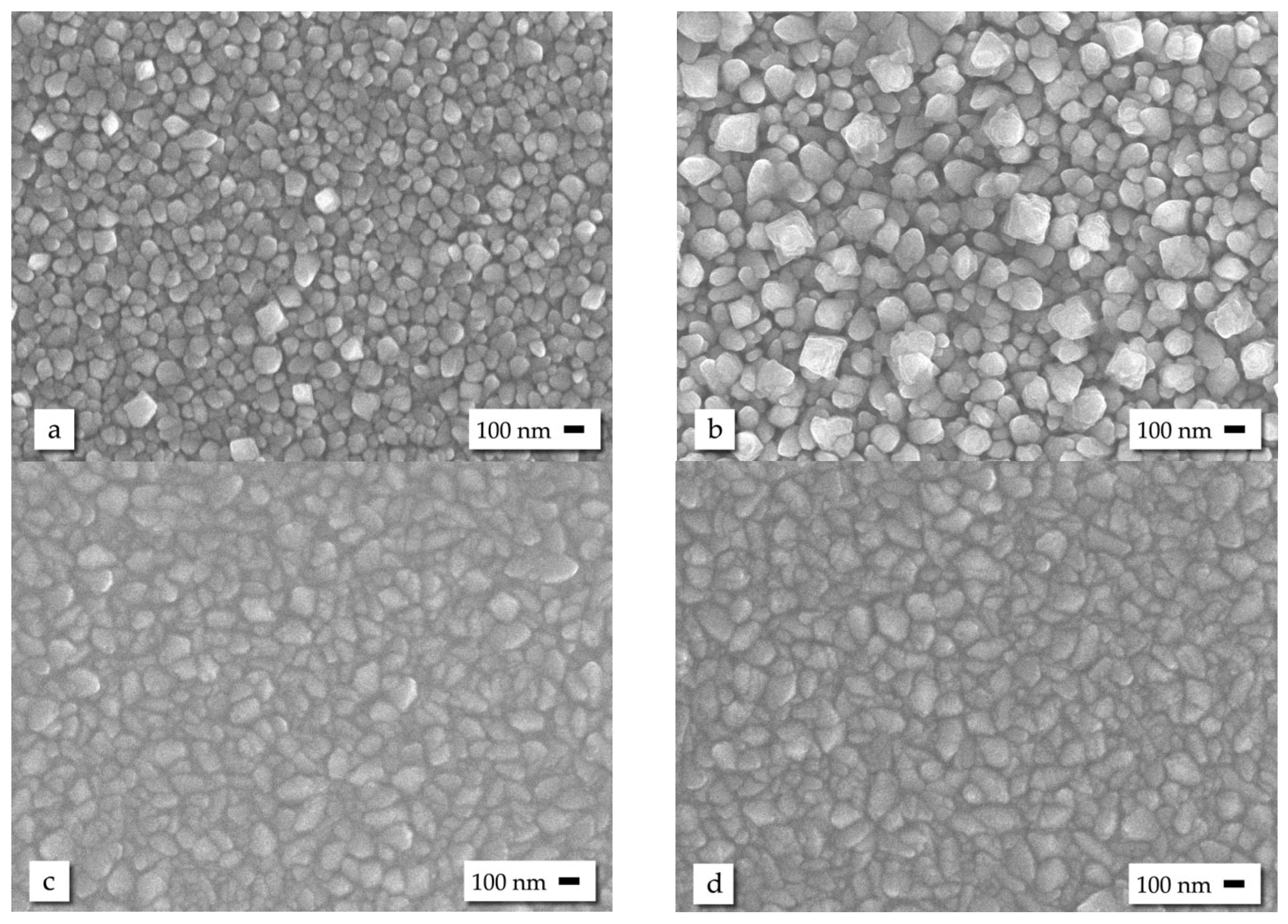
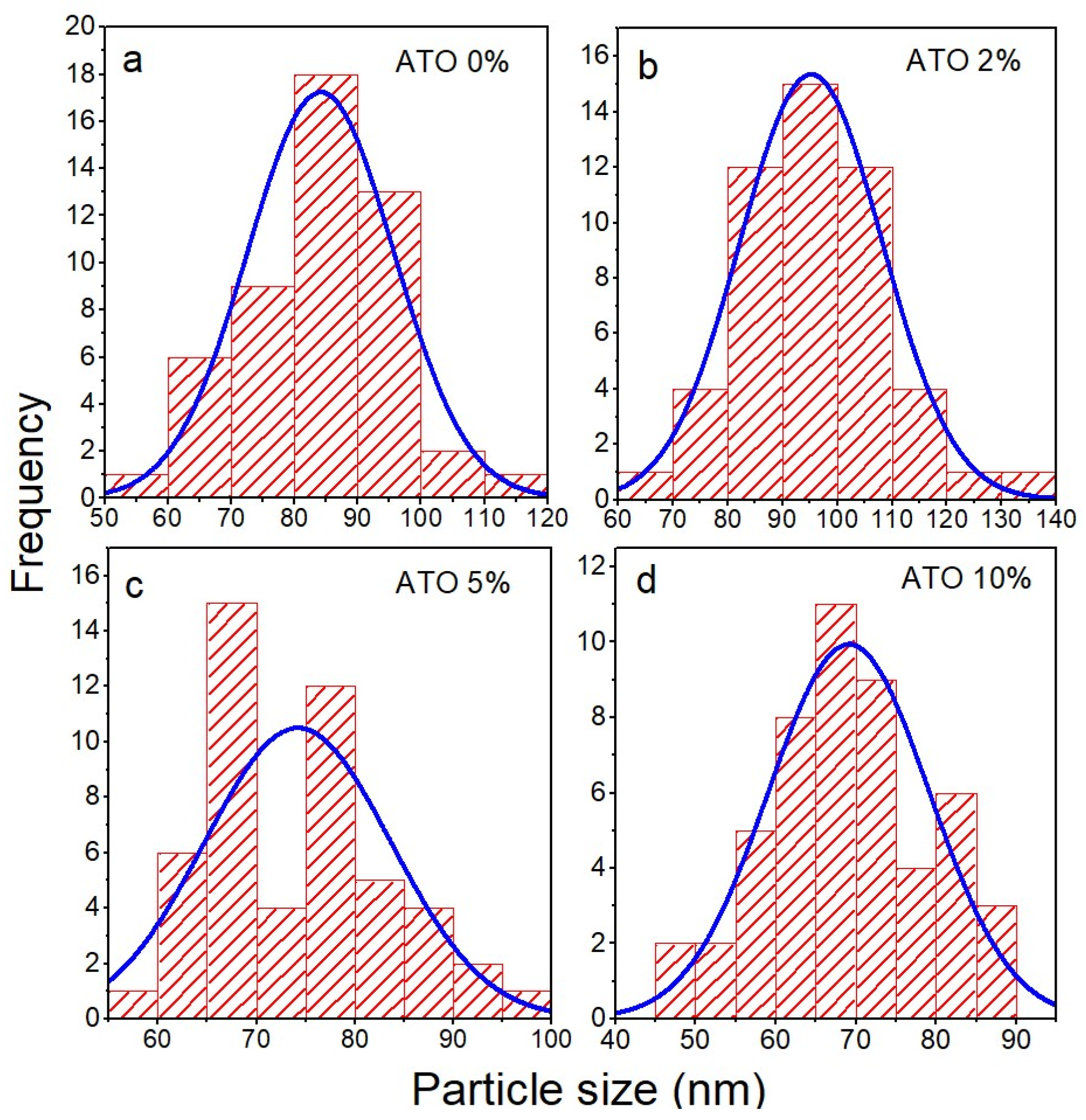
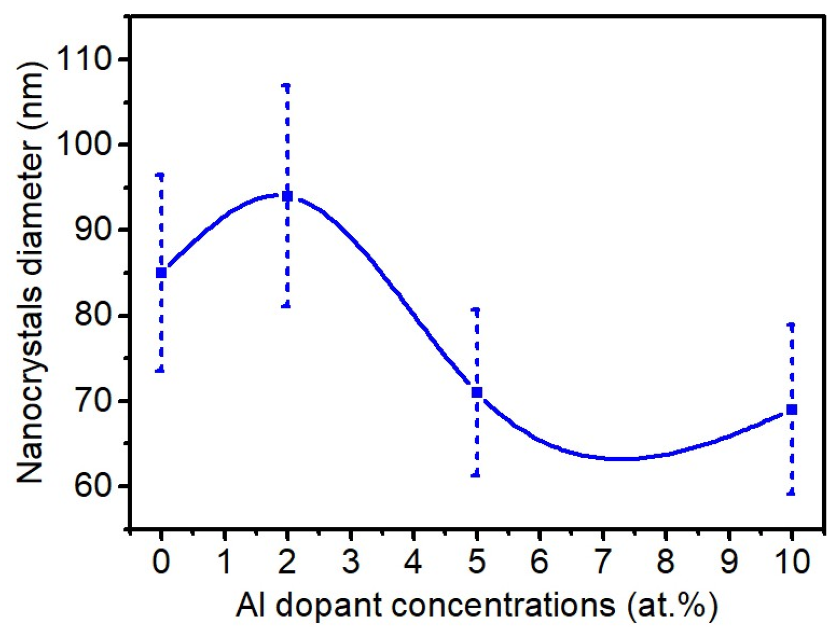
3.1. Scannig Electron Microscopy

SEM images of ATO films with varying aluminum percentages (0, 2, 5, and 10 at. %) are shown in Figure 1. The images indicate that at doping levels of 0 and 2 at. % Al, the material consists of relatively fine spherical nanoparticles. In contrast, at doping levels of 5 and 10 at. % Al, there is a noticeable reduction in sphericity, leading to signs of agglomeration. Figure 2 displays the particle size distribution graph for the ATO samples with varying doping levels. Each sample’s average particle size distribution (Figure 2, striped red bars) is fitted using a Gaussian function (Figure 2, blue curve), where the peak value indicates the average size of the particles. The average grain size in undoped SnO2 film (0 at. % Al) was measured at 85 ± 11 nm (Figure 1a). Although the SEM image of ATO doped with 2 at. % Al may imply an increase in nanoparticle size, it is noted that while some larger nanoparticles are present the majority are smaller, resulting in an average size of approximately 90 ± 13 nm (Figure 1b and Figure 2b). As the doping level increases to 5 and 10 at. % Al, the average grain sizes decrease to 71 ± 9 nm and 69 ± 9 nm, respectively (Figure 1c,d). The observed reduction in average grain size in the doped ATO films, ranging from 90 ± 13 nm to 69 ± 9 nm, is attributed to the increase in the density of crystallization centers within the film. Additionally, another contributing factor may be the increased compressive stress in the ATO films, caused by the substitution of Sn4+ ions (ionic radius of 0.71 Å) with Al3+ ions (ionic radius of 0.51 Å) [29,32,33]. The calculated error indicates that the size of the nanoparticles is not uniform, especially in ATO:0 at. % Al and ATO:2 at. % Al. As the doping level increases, the size of the nanoparticles becomes more uniform compared to lower doping levels Figure 2 and Figure 3, where the continuous curve represents the average value, and the vertical dash lines represent the error in the size of the nanoparticle (Figure 3).
The elemental compositions of the ATO samples were examined using EDS, confirming that the samples consisted solely of Sn, Al, and O, along with a minor carbon peak, primarily linked to the organic materials used in the synthesis process and the heat treatment applied to the samples.

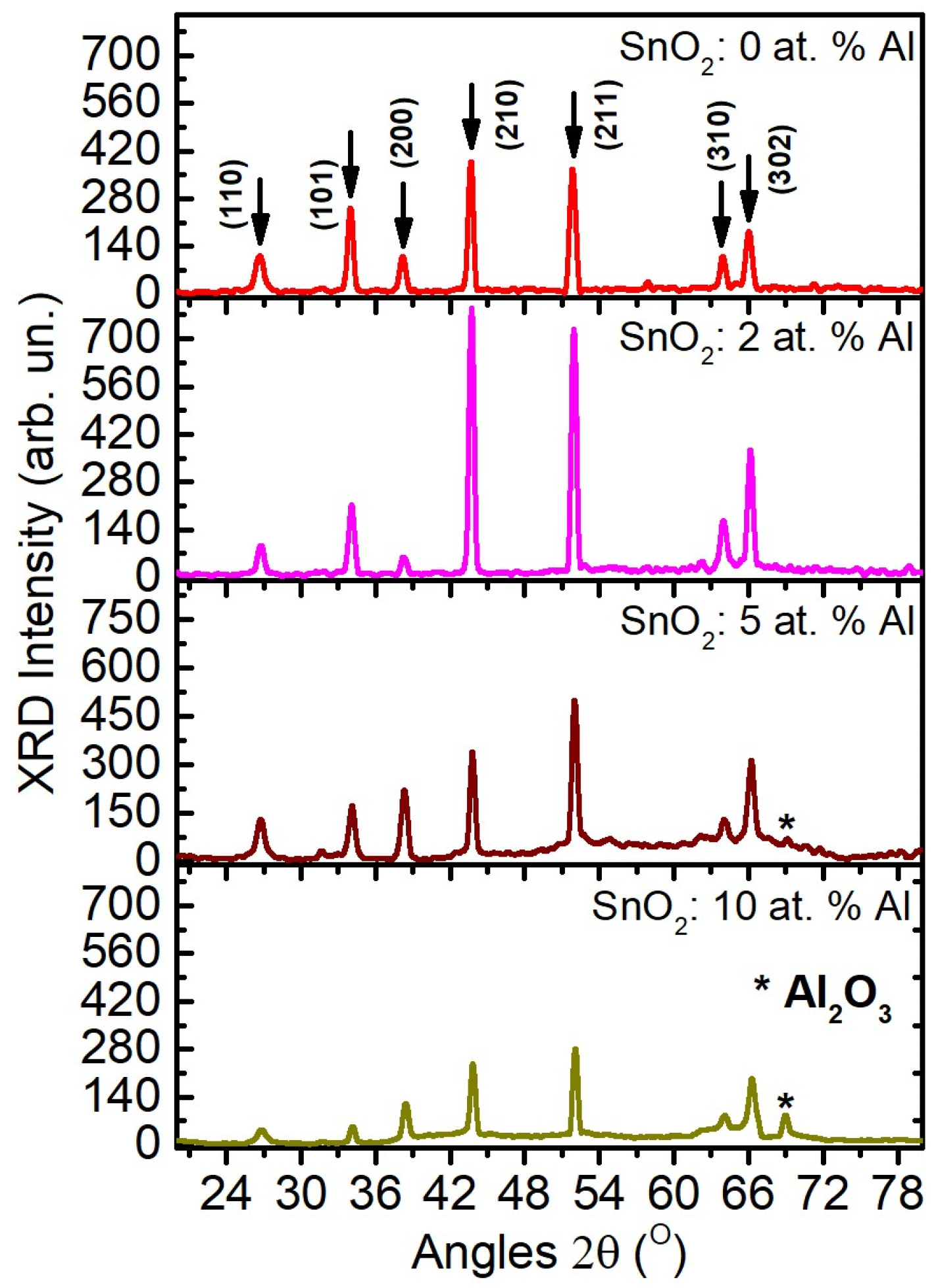
3.2. X-Ray Diffraction

The X-ray diffraction (XRD) patterns of the ATO nanocrystal films are illustrated in Figure 3. Analyzing the XRD patterns reveals that the SnO2 film (0 at. % Al) display XRD peaks at 2θ = 26.693°, 34.026°, 38.304°, 43.743°, 51.969°, 57.995°, 63.938°, 66.028°, and 71.403°, which correspond to the X-ray diffraction from the (110), (101), (200), (210), (211), (002), (310), (301), and (202) planes, respectively, in a tetragonal polycrystalline structure (ICDD file no. 00-002-1340). The presence of multiple XRD peaks suggests that a polycrystalline film is present. The nearly identical intensity of these peaks indicates that the X-ray diffraction in the (101), (210), and (211) planes is the most dominant, with the remaining peaks exhibiting lower intensity. Additionally, there are more nanocrystals oriented in the (101), (210), and (211) planes compared to the other nanocrystals in the ATO films. The intensity of the XRD peaks at 2 at. % Al-doped ATO films is greater than that of the other ATO samples (Figure 4), indicating that the highest crystallinity is achieved in the 2 at. % ATO sample; thereafter, the intensity declines, suggesting the deterioration of the ATO unit cell. As the Al content in the ATO films increases, the XRD peaks shift to higher angles, signifying a reduction in interplanar distances and crystal lattice parameters of the ATO films (Table 1).
The unit cell parameters a and c were estimated using Bragg’s law ( n λ = 2 d h k l sin θ ) and the established relation ( d h k l 2 = h 2 + k 2 a 2 + l 2 c 2 ). The calculations for the ATO lattice parameters a and c utilized the peak positions of the (110) and (101) planes in the XRD pattern, with a = λ 2 sin θ 1 and c = 2 sin θ 2 λ 2 a 2 0.5 formulas applied. The parameters a and c of the crystalline unit cells in ATO films decrease as the Al doping increases, as shown in Table 1. By incorporating the aluminum ion into the unit cell of tin oxide, which has a smaller radius than that of the tin ion, the aluminum ion occupies a reduced volume within the crystal structure of SnO2. To accommodate the aluminum ions, adjacent ions shift inward, leading to a decrease in the distance between them and, consequently, a reduction in the unit cell parameters of ATO. As previously mentioned, the change in the crystal lattice parameter results from the smaller ionic radius of Al3+ ions (0.51 Å) in comparison to that of Sn4+ ions (0.71 Å). In the ATO samples with doping levels ranging from 0 at. % to 2 at. %, no secondary phase was observed, indicating that aluminum ions were completely integrated into the unit cell of tin oxide. In the ATO at 5 at. % and ATO at 10 at. % samples, a secondary phase was detected at the angle of 2 θ at 69°, corresponding to the Miller plane (224) of Al2O3 in its hexagonal crystalline form. For ATO at 5 at. %, the peak observed at 69° has a lower intensity compared to the same peak seen in ATO at 10 at. %, suggesting that between 2 at. % and 5 at. % there is a saturation process occurring, leading to the emergence of a secondary phase (ICDD file no. 00-010-0414).

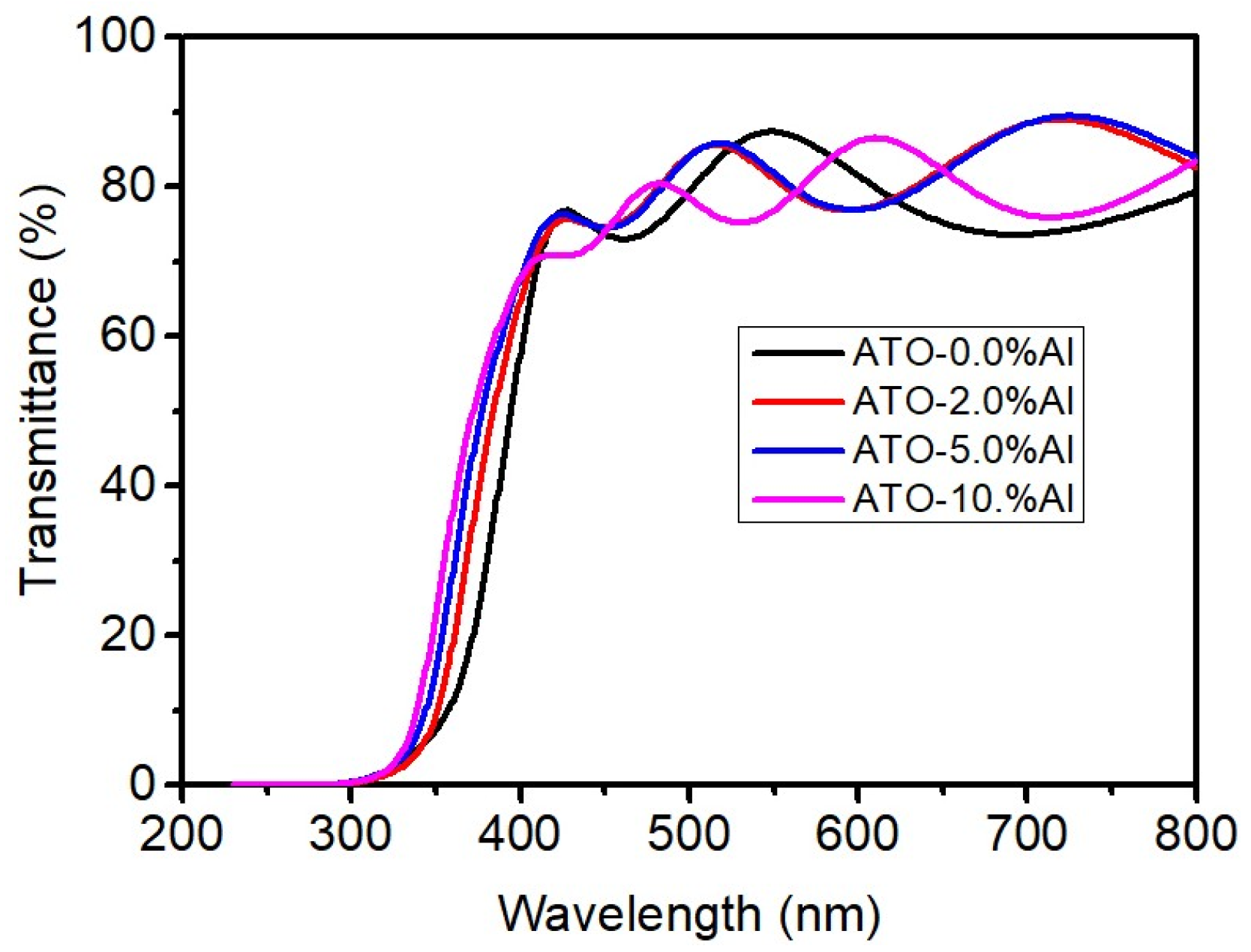
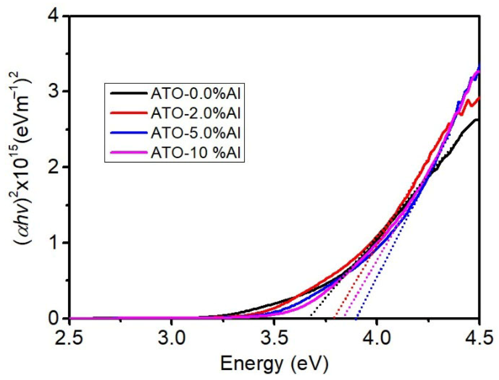
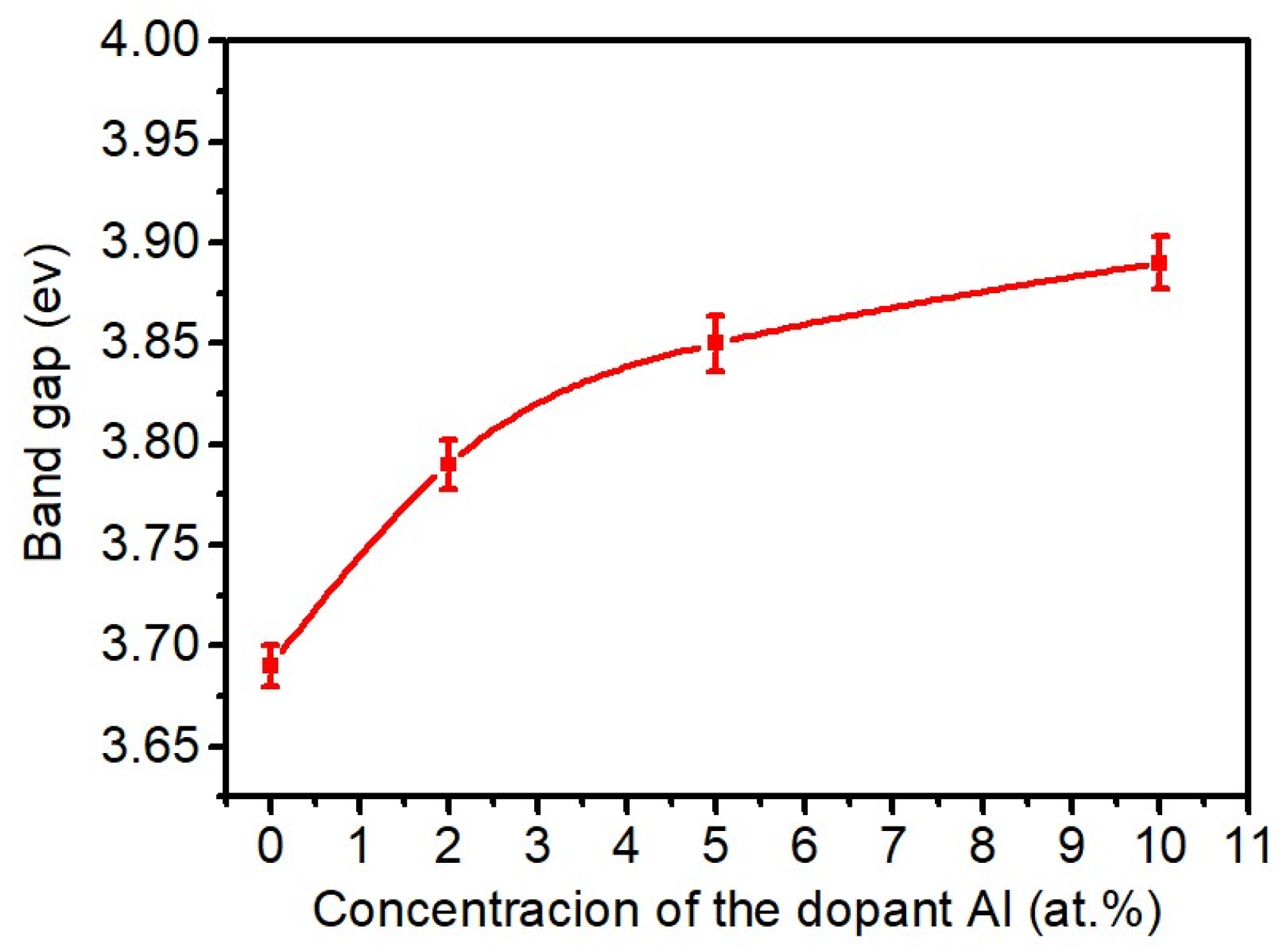
3.3. Transmittance and Bad Gap

The transmittance spectra for both SnO2 and ATO films are shown in Figure 5. Measurements were conducted over a spectral range of 200–800 nm. The transmittance levels of the ATO films range from approximately 75% to 85%. The variations noted in the transmittance spectra are attributed to light interference at the interface between the ATO film and the quartz substrate. To assess the bandgap Eg, it is important to note that the film thickness does not influence the transmittance measurement technique; thus, measurements were taken at three different locations using the following Tauc Equation (1) [33]:
α h ν = A h ν E g n
where n equals 1/2 for a direct transition, α represents the absorption coefficient (m−1), A is a constant, denotes the incident photon energy (eV), and Eg (eV) refers to the bandgap. By plotting (α)2 (eVm−1)2 against , a straight line can be projected onto the energy axis; the intersection point with the energy axis provides the value of the bandgap Eg. Utilizing three transmittance measurements and the Tauc equation, the potential values for Eg were determined, as shown in Figure 5 and Figure 6. At a doping level of 0 at. % Al, the average bandgap was measured at 3.69 ± 0.01   eV . For the 2 at. % Al condition, the bandgap value was 3.79 ± 0.012   eV . In the case of doping levels of 5 at. % Al and 10 at. % Al, the energy gap values were 3.85 ± 0.014   eV and 3.79 ± 0.013   eV , respectively.
For low-dimensional materials, their bandgap is generally larger than that of the same material in bulk, a phenomenon attributed to the quantum confinement effect [33,36]. This behavior can be readily inferred from the following Equation (2):
E g = E g o + π 2 2 μ R 2
where E g o is the bandgap energy of the bulk material, which is around 3.60 eV for tin oxide, μ is the reduced effective mass, is the reduced Planck constant, E g is the bandgap of the material in its nanometric form, and R is the radius of the nanoparticles. From Equation (2) it can be concluded that as R decreases, i.e., having a low-dimensional material, the bandgap increases, and the larger R is then the closer the bandgap becomes to the value of E g o . The results obtained from the XRD analysis where the ATO lattice parameters decrease (Table 1) and those from the analysis of the SEM images that show that the size of the nanoparticles decreases are both consistent when the Al dopant content increases. From Figure 6 and Figure 7, the increase in the bandgap from 2 at. % to 5 at. % sharply increases, and between 5 at. % and 10 at. % for the doping level the increase in Eg smoothly increases. All the transmittance results (Eg calculation) are consistent with SEM and XRD studies and agree with Equation (2) of quantum confinement. The rise in the optical bandgap of ATO films with higher Al doping content, along with the reduction in lattice parameters and average nanoparticle size, is consistent across all these findings. It is important to highlight that our results on ATO films produced through the ultrasonic spray pyrolysis method align with the results documented in existing literature.

4. Conclusions

Thin films of tin oxide doped with aluminum were synthesized using the ultrasonic spray pyrolysis technique. The effect of varying aluminum concentrations on the structural, optical, and morphological properties of the ATO films was investigated. The semiconductor films exhibited a polycrystalline tetragonal structure without a clear preferential orientation. A slight shift toward higher angles was observed as the doping level increased, indicating a reduction in the a and c unit cell parameters. Additionally, the intensity of the XRD patterns decreased, suggesting the beginning of unit cell destruction in the ATO samples. In the doping range of 0–2 at. %, no secondary phase was evident; however, for a 5 at. % aluminum doping level the onset of Al2O3 formation was detected. It was determined that to prevent a secondary phase the doping level must remain below 5 at. % in the ATO samples. Analysis of the SEM images and nanoparticle size distribution showed a gradual decrease in average grain size, particularly between doping levels of 2 at. % and 10 at. %. Transmittance analysis revealed transparency levels ranging from 75% to 85% in the visible spectral range for the analyzed films. Furthermore, an increase in the bandgap was observed, ranging from 3.69 to 3.85 eV, a result attributed to the reduction in lattice parameters (confirmed with XRD) and the average nanoparticle size (Equation (2)) of the ATO films due to the increased concentration of aluminum ions in the samples.

Author Contributions

Methodology, U.G.T. and A.I.D.C.; validation, A.I.D.C. and B.E.F.; formal analysis, B.E.F. and I.C.B.R. investigation, B.E.F., U.G.T., M.B. and I.C.B.R.; writing—original draft preparation, B.E.F. and I.C.B.R.; writing—review and editing, I.C.B.R., M.B., A.I.D.C. and B.E.F. All authors have read and agreed to the published version of the manuscript.

Funding

The partial financial support from SECIHTI Mexico and SIP-IPN (20240120, 20240156 and 20253774) has been secured.

Data Availability Statement

The authors confirm that all data supporting the findings of this study are available within the article.

Acknowledgments

The authors would like to express their sincere gratitude to SECIHTI Mexico and SIP-IPN, Mexico (20240120, 20240156 and 20253774) for their generous financial support. Additionally, the authors wish to acknowledge CNMN-IPN for conducting the measurements, with special thanks to Hugo Martinez Gutierrez for his assistance with the SEM measurements.

Conflicts of Interest

The authors declare no conflicts of interest.

References

  1. Rozati, S.M.; Ziabari, S.A.M. A review of various single layer, bilayer, and multilayer TCO materials and their applications. Mater. Chem. Phys. 2022, 292, 1–24. [Google Scholar] [CrossRef]
  2. Jarzebski, Z.M.; Marton, J.P. Physical properties of SnO2 materials: II. Electrical properties. J. Electrochem. Soc. 1976, 123, 299C–310C. [Google Scholar] [CrossRef]
  3. Amutha, T.; Rameshbabu, M.; Sasi Florence, S.; Senthilkumar, N.; Vetha Potheher, I.; Prabha, K. Studies on structural and optical properties of pure and transition metals (Ni, Fe and co-doped Ni–Fe) doped tin oxide (SnO2) nanoparticles for anti-microbial activity. Res. Chem. Intermed. 2019, 45, 1929–1941. [Google Scholar] [CrossRef]
  4. Tazikeh, S.; Akbari, A.; Talebi, A.; Talebi, E. Synthesis and characterization of tin oxide nanoparticles via the Co-precipitation method. Mat. Sci.-Pol. 2014, 32, 98–101. [Google Scholar] [CrossRef]
  5. Calnan, S.; Tiwari, A.N. High mobility transparent conducting oxides for thin film solar cells. Thin Solid Film. 2010, 518, 1839–1849. [Google Scholar] [CrossRef]
  6. Granqvist, C.G. Transparent conductors as solar energy materials: A panoramic review. Sol. Energy Mater. Sol. Cells 2010, 91, 1529–1598. [Google Scholar]
  7. Wang, C.; Cui, X.; Liu, J.; Zhou, X.; Cheng, X.; Sun, P.; Lu, G. Design of superior ethanol gas sensor based on Al-doped NiO nanorod-flowers. ACS Sens. 2016, 1, 131–136. [Google Scholar] [CrossRef]
  8. Samson, S.; Fonstad, C.G. Defect structure and electronic donor levels in stannic oxide crystals. J. Appl. Phys. 1973, 44, 4618–4621. [Google Scholar] [CrossRef]
  9. Deyu, G.K.; Muñoz-Rojas, D.; Rapenne, L.; Deschanvres, J.-L.; Klein, A.; Jiménez, C.; Bellet, D. SnO2 films deposited by ultrasonic spray pyrolysis: Influence of Al incorporation on the properties. Molecules 2019, 24, 2797–2812. [Google Scholar] [CrossRef]
  10. Lei, M.; Hu, Q.R.; Wang, S.L.; Tang, W.H. Structural and optical properties of Al-doped SnO2 nanowires. Mat. Lett. 2010, 64, 19–21. [Google Scholar] [CrossRef]
  11. Weidner, M.; Jia, J.; Shigesato, Y.; Klein, A. Comparative study of sputter-deposited SnO2 films doped with antimony or tantalum: Comparative study of sputter-deposited SnO2:Sb and SnO2:Ta. Phys. Status Solidi. B Basic Res. 2016, 253, 923–928. [Google Scholar] [CrossRef]
  12. Weidner, M.; Fuchs, A.; Bayer, T.J.M.; Rachut, K.; Schnell, P.; Deyu, G.K.; Klein, A. Defect modulation doping. Adv. Funct. Mater. 2019, 29, 11467–11479. [Google Scholar] [CrossRef]
  13. White, M.E.; Bierwagen, O.; Tsai, M.Y.; Speck, J.S. Electron transport properties of antimony doped SnO2 single crystalline thin films grown by plasma-assisted molecular beam epitaxy. J. Appl. Phys. 2009, 106, 093704–093710. [Google Scholar] [CrossRef]
  14. Dai, C.M.; Su, C.S.; Chuu, D.S. Growth of highly oriented tin oxide thin films by laser evaporation deposition. Appl. Phys. Lett. 1990, 57, 1879–1881. [Google Scholar] [CrossRef]
  15. Kane, J.; Schweizer, H.; Kern, W. Chemical Vapor Deposition of Antimony-Doped Tin Oxide Films Formed from Dibutyl Tin Diacetate. J. Electrochem. Soc. 1976, 123, 270–277. [Google Scholar] [CrossRef]
  16. Lee, S.-H.; Choi, J.-M.; Lim, J.-H.; Park, J.; Park, J.-S. A study on the thermoelectric properties of ALD-grown aluminum-doped tin oxide with respect to nanostructure modulations. Ceram. Int. 2018, 44, 1978–1983. [Google Scholar] [CrossRef]
  17. Terán, U.G.; Díaz Cano, A.I.; Torchynska, T.; Rodriguez, I.C.B.; El Filali, B.; Cervantes, J.E. Impact of Cu doping on morphology, structural and optical characteristics of SnO2 thin films prepared by spray pyrolysis. MRS Adv. 2024, 9, 1849–1853. [Google Scholar] [CrossRef]
  18. Bilgin, V.; Akyuz, I.; Ketenci, E.; Kose, S.; Atay, F. Electrical, structural and surface properties of fluorine doped tin oxide films. Appl. Surf. Sci. 2010, 256, 6586–6591. [Google Scholar] [CrossRef]
  19. Saoula, I.; Siad, C.; Djedidi, K.; Allag, N.; Chala, A. Effect of (Al, Zn, Cu, and Sr) doping on structural, optical and electrical properties of sprayed SnO2 thin films. Acta Metall. Slovaka 2023, 29, 59–62. [Google Scholar] [CrossRef]
  20. Rodriguez, I.C.B.; El Filali, B.; Torchynska, T.; Douda, J.; Ibarra, I.C.R. Optical and structural properties of Sn doped ZnO thin films synthesized by spray pyrolysis. MRS Adv. 2023, 8, 1434–1437. [Google Scholar] [CrossRef]
  21. Minami, T.; Miyata, T.; Ohtani, Y.; Kuboi, T. Effect of thickness on the stability of transparent conducting impurity-doped ZnO thin films in a high humidity environment. Phys. Status Solidi Rapid Res. Lett. 2007, 1, R31–R33. [Google Scholar] [CrossRef]
  22. Lee, S.-H.; Kwon, K.; Kim, K.; Yoon, J.S.; Choi, D.-S.; Yoo, Y.; Kim, C.; Kang, S.; Kim, J.H. Electrical, structural, optical, and adhesive characteristics of aluminum-doped tin oxide thin films for transparent flexible thin-film transistor applications. Materials 2019, 12, 137–142. [Google Scholar] [CrossRef]
  23. Zhang, J.; Wei, X.; Miao, J.; Zhang, R.; Zhang, J.; Zhou, M.; Lu, W. Enhanced performance of an Al-doped SnO2 anode for the electrocatalytic oxidation of organic pollutants in water. Mater. Today Commun. 2020, 24, 101164–101172. [Google Scholar] [CrossRef]
  24. Salameh, B.; Alsmadi, A.M.; Hegazy, A.R. Optoelectronic properties and optical transitions in low concentrated aluminum-doped tin oxide thin films. J. Alloys Compd. 2023, 969, 172412–172424. [Google Scholar] [CrossRef]
  25. Doyan, A.; Susilawati, I.Y.D.; Gunawan, E.R.; Taufik, M. Characterization thin film nano particle of aluminum tin oxide (AlTO) as touch screen. J. Phys. Conf. Ser. 2018, 1097, 012009–012017. [Google Scholar] [CrossRef]
  26. Wei, C.; Zhang, G.; Bai, Y.; Yan, D.; Yu, C.; Wan, N.; Zhang, W. Al-doped SnO2 hollow sphere as a novel anode material for lithium-ion battery. Solid State Ion. 2015, 272, 133–137. [Google Scholar] [CrossRef]
  27. Wang, E.; Chen, P.; Yin, X.; Wu, Y.; Que, W. Tailoring electronic properties of SnO2 quantum dots via aluminum addition for high-efficiency perovskite solar cells. Solar RRL. 2019, 3, 1900041–1900410. [Google Scholar] [CrossRef]
  28. Duan, Y.; Zheng, J.; Fu, N.; Fang, Y.; Liu, T.; Zhang, Q.; Zhou, X.; Lin, Y.; Pan, F. Enhancing the performance of dye-sensitized solar cells: Doping SnO2 photoanodes with Al to simultaneously improve conduction band and electron lifetime. J. Mater. Chem. A Mater. Energy Sustain. 2015, 3, 3066–3073. [Google Scholar] [CrossRef]
  29. Soussi, A.; Haounati, R.; Aithssi, A.; Taoufiq, M.; Baoubih, S.; Jellil, Z.; El hankari, S.; Elfanaoui, A.; Markazi, R.; Ihlal, A. Investigating structural, morphological, electronic, and optical properties of SnO2 and Al-doped SnO2: A combined DFT calculation and experimental study. Phy. B Cond. Matt. 2024, 690, 416242–416251. [Google Scholar] [CrossRef]
  30. Bouabdalli, E.; El Jouad, M.; Garmim, T.; Louardi, A.B.; Hartiti, B.; Monkade, M.; Touhtouh, S.; Hajjaji, A. Elaboration and characterization of Ni and Al co-doped SnO2 thin films prepared by spray pyrolysis technique for photovoltaic applications. Mat. Sci. Eng. B 2022, 286, 116044–116053. [Google Scholar] [CrossRef]
  31. Suvarna, T.; Reddy, K.G.; Mohan, V.M.; Lavanya, G.; Ramana Reddy, M.V.R.; Vardhani, C.P. Investigation on Sb-doped SnO2 as an efficient sensor for the detection of formaldehyde. Inorg. Chem. Comm. 2024, 167, 112748–112759. [Google Scholar] [CrossRef]
  32. Abvarza, B.; Alehdaghia, H.; Ziraka, M. Preparation of Al-doped SnO2 thin films via ultrasonic mist vapor deposition method: Optimization the growth parameters towards a superhydrophobic layer. Phy. B Cond. Matt. 2025, 712, 417240–417251. [Google Scholar] [CrossRef]
  33. Mallick, H.K.; Zhang, Y.; Pradhan, J.; Sahoo, M.P.K.; Pattanaik, A.K. Influence of particle size and defects on the optical, magnetic and electronic properties of Al doped SnO2 nanoparticles. J. Alloys Compd. 2021, 854, 156067–156077. [Google Scholar] [CrossRef]
  34. Sayeed, M.A.; Rouf, H.K. Al-doped SnO2 thin films: Impacts of high temperature annealing on the structural, optical and electrical properties. J. Mat. Res. And Tech. 2021, 15, 3409–3425. [Google Scholar] [CrossRef]
  35. Ausama, I.K.; Attarid, M.O. Influence of the aluminum doping on the physical and gas sensing properties of SnO2 for H2 gas detection. Sens. Actuators B Chem. 2021, 340, 129633–129640. [Google Scholar]
  36. Kar, A.; Kundu, S.; Patra, A. Surface Defect-Related Luminescence Properties of SnO2 Nanorods and Nanoparticles. J. Phys. Chem. 2011, 115, 118–124. [Google Scholar] [CrossRef]
Figure 1. SEM images of ATO films with different Al contents: (a) 0 at. %, (b) 2 at. %, (c) 5 at. %, and (d) 10 at. %.
Jcs 09 00358 g001
Figure 2. Nanoparticle size distribution for ATO samples: (a) 0 at. %, (b) 2 at. %, (c) 5 at. %, and (d) 10 at. %.
Jcs 09 00358 g002
Figure 3. Nanocrystals size of ATO thin films.
Jcs 09 00358 g003
Figure 4. The XRD patterns of ATO thin films.
Jcs 09 00358 g004
Figure 5. Transmittance spectra of ATO films.
Jcs 09 00358 g005
Figure 6. Bandgap energy spectra of ATO films.
Jcs 09 00358 g006
Figure 7. Variation in bandgap energy spectra ATO films.
Jcs 09 00358 g007
Table 1. The variation in XRD peak positions and lattice parameters with Al contents.
Sample(110)(101)(200)(210)(211)(310)(302)a (Å)c (Å)
ATO:0.0Al26.6633.9838.2443.6551.8463.9466.044.7243.176
ATO:2.0Al26.7534.0838.2843.7351.9664.0066.174.7093.168
ATO:5.0Al26.7834.1238.3643.8452.0364.1266.284.7043.164
ATO:10.0Al26.8434.1838.4543.8552.1364.1466.324.6933.159
Disclaimer/Publisher’s Note: The statements, opinions and data contained in all publications are solely those of the individual author(s) and contributor(s) and not of MDPI and/or the editor(s). MDPI and/or the editor(s) disclaim responsibility for any injury to people or property resulting from any ideas, methods, instructions or products referred to in the content.

