Article

Modeling Piezoresistive Behavior of Conductive Composite Sensors via Multi-State Percolation Theory

by
Nathan S. Usevitch
1,
Emily V. White
2,
Anton E. Bowden
1,
Ulrike H. Mitchell
3 and
David T. Fullwood
1,*
1
Mechanical Engineering Department, Brigham Young University, Provo, UT 84602, USA
2
Independent Researcher, West Allis, WI 53219, USA
3
Department of Exercise Sciences, Brigham Young University, Provo, UT 84602, USA
*
Author to whom correspondence should be addressed.
J. Compos. Sci. 2025, 9(7), 354; https://doi.org/10.3390/jcs9070354
Submission received: 19 May 2025 / Revised: 26 June 2025 / Accepted: 4 July 2025 / Published: 8 July 2025
(This article belongs to the Special Issue Characterization and Modelling of Composites, Volume III)

Abstract

Flexible strain sensors, fabricated from high-elongation polymers and conductive filler particles, are proving an essential tool in the study of biomechanics using wearable technology. It has been previously shown that the resistive response of such composites, relative to the amount of conductive filler material, can be reasonably modeled using a standard percolation-type model. Once a certain critical fraction of filler material is reached, a conductive network across the sample is established and resistance rapidly decreases. However, modeling the more subtle resistance changes that occur while deforming the sensors during operation is more nuanced. Conductivity across the network of particles is dominated by tunneling mechanisms at the interfaces between the filler materials. Small changes in strain at these interfaces lead to relatively large, but nevertheless continuous, changes in local resistance. By assigning some arbitrary value of resistance as a dividing line between ‘low’ and ‘high’ resistance, one might model the piezoresistive behavior using a standard percolation model. But such an assumption is likely to lead to low accuracy. Our alternative approach is to divide the range of potential resistance values into several bins (rather than the usual two bins) and apply a relatively novel multi-state percolation theory. The performance of the multi-state percolation model is assessed using a random resistor model that is assumed to provide the ground truth. The model is applied to predict resistance response with both changes in relative amount of conductive filler (i.e., to help design the initial unstrained sensor) and with applied strain (for an operating sensor). We find that a multi-state percolation model captures the behavior of the simulated composite sensor in both cases. The multicomponent percolation theory becomes more accurate with more divisions/bins of the resistance distribution, and we found good agreement with the simulation using between 10 and 20 divisions.

1. Introduction

1.1. Piezoresistive Nano-Composites

Nano- and micro-composites with conductive filler particles show great promise as multifunctional materials. Applications of such materials are varied and include lightning strike protection, electromagnetic field shielding, and self-sensing materials [1,2,3,4]. One prominent application that will be the focus of this paper is the development of piezoresistive composites for use as high-elongation strain gauges [5,6,7,8]. Applications include skin and fabric mounted arrays for tracking human biomechanics in a variety of situations (e.g., [9]).
Percolation-type models are obvious solutions for modeling the overall conductivity of this type of conductive composite, due to the large contrast in electrical properties between the base polymer and the filler material (e.g., [10]). As the fraction of conductive filler increases beyond a certain critical level (the percolation threshold), connected paths of filler particles can be found that span the sample, and the conductivity rises rapidly with the addition of more filler. However, modeling the relationship between applied strain and conductivity is more complex. As deformation occurs, gaps between individual particles expand or contract, and the local resistance is modified by a quantum tunneling model. Such behavior can be coarsely captured by assuming that a particular gap is ‘conducting’ when the gap resistance is below a certain value, and non-conducting when the resistance exceeds that value—enabling the use of standard percolation models [11,12]. However, such an approach is a gross oversimplification of the actual relationship between local deformation and conductivity. In this study, the accuracy of such a model is explored, and an improved model using multi-state percolation (as opposed to the usual binary-state percolation) is proposed.
Piezoresistive conductive composites are generally composed of small conductive particles or fibers randomly oriented in an insulating polymer matrix. Self-sensing materials composed of nickel nano-strands embedded in a polymer matrix have been developed by the authors [13], but many other options are possible (see some of the papers and review mentioned above). An example image of nickel nano-strands before embedding into a composite material can be seen in Figure 1. When randomly oriented in an insulating polymer, these conductive nano-strands form a complex three-dimensional network with many potential electrical connections between individual nano-strands. This structure imparts electrical conductivity that changes with mechanical deformation, even at extremely low volume fractions of conductive particles. As mentioned, the relationship between volume fraction of filler and resultant conductance is typically modeled using percolation theory [10]; as more filler is added, a critical volume is reached where connected clusters of filler begin to span the entire sample [14].
A representative problem in percolation theory involves determining the flow rate of a liquid through a porous medium. It is assumed that only a certain fraction of pores have open connections to neighboring pores. Below the so-called percolation threshold of open connections, no water will flow through the medium; but as the number of connections rises above this threshold it will become statistically certain that an open pathway exists that spans the sample, allowing the liquid to flow. The theory can be applied to many physical situations, including grain boundary diffusion, transmission of signals, strength of randomly oriented composite materials, charge transfer through a network of resistors, and many other systems [14,15,16].
In certain systems, resistance to flow across each branch of the network changes discretely, as in the porous rock example where each branch of the network is either open or closed. However, in many physical networks, resistance to flow across a particular branch may change in a more continuous manner. For example, local diffusivity or electrical resistance may often take on a continuous range of values, but instead, discrete binary values are assigned in order to allow standard percolation theory to be applied. To address this issue, Chen and Schuh proposed a model for a multi-state percolation theory and applied this model to the problem of grain boundary diffusion [17].
For the materials of interest in this study, it is typically assumed that a layer of insulating polymer is adsorbed onto each conductive particle, such that no two conductive particles are in full electrical contact, but are separated by a nano-scale gap [18,19]. Charge transfer across these nano-gaps (tunneling junctions) occurs primarily through quantum tunneling of electrons between the conductive particles. The resultant local conductivity changes continuously with gap size and implies that a small change in gap dimension can result in a large change in resistance [11,20]. Since the resistivity of the conductive particles is low compared to that of the gaps, it is assumed that the macro conductance of the composite is primarily governed by the characteristics of these tunneling gaps, as opposed to the electrical properties of the conductive phase. There has been significant work conducted by others to examine the effect of percolation in systems in which tunneling occurs [21,22]. Based on this prior work, the resistivity of a single gap between conductive particles to electron tunneling is estimated by the following equation [23,24]:
r t = h 2 e 2 2 m λ exp 4 π 2 m λ h s
where r t represents the electrical resistance across a gap, h is Planks constant, m is the mass of an electron, s is the gap distance between conductive particles, e is the charge of an electron, and λ is the tunneling barrier height for the polymer/nickel combination (J). Accurate values of λ are not readily available for most materials, but new methods have been developed to experimentally measure the barrier height of various material combinations [18]. We note that in the study of percolating systems, it is more common to deal with conductivity rather than resistivity, so future references in this paper will be made primarily to gap conductivity, the inverse of gap resistivity. Conductivity is converted to conductance by assuming that a representative contact patch is approximately square with 300 nm side length, where 300 nm is an approximation for the diameter of one of the nano-strands. Represented graphically, it can be seen that the conductance of a gap decreases rapidly with increasing gap distance (Figure 2), thus helping explain the large changes in material conductance with strain.

1.2. Classical Models

Classical percolation theory focuses on the study of high contrast systems. In a conductive nano-composite, a high contrast is typically present since the matrix is generally assumed to be perfectly insulating, and the filler material is highly conductive. The effective electrical conductivity of the composite network is defined as the equivalent conductivity of the network if it were represented by a single component. Using percolation theory, the effective conductivity ( σ e f f ) of the system is defined by the following relationships [17,25]:
σ e f f p p c s f o r   p <   p c σ e f f p p c t f o r   p > p c
where pc is the percolation threshold, p is the volume fraction of conductive material, and t and s are universal scaling exponents. The percolation threshold is a parameter dependent only on the geometry of the network; it represents the volume fraction at which the probability is 1 that a network of conducting links spans an infinite network [14].
An alternative percolation-type model, McLachlan’s General Effective Medium approach (GEM), defines effective conductance for systems of non-perfect contrast, i.e., when the conductivity of the insulating phase, σ i , is not 0. Effective conductance, σ m , is defined implicitly in the following equation:
1 p σ i   1 s σ m 1 s σ i   1 s + A σ m 1 s + ( p ) σ c   1 t σ m 1 t σ c   1 t + A σ m 1 t = 0 where A = 1 p c p c
In this equation, p is the fraction of conductive links, σi and σc are the conductance of the insulating and conductive phase, respectively, and pc is the percolating threshold. The exponents s and t are nominally the same universal scaling exponents used in classical percolation (see Equation (2)). However, considerable work has been conducted in this area and has shown that these exponents often have non-universal values [26]. For systems of non-perfect contrast, values had been reported to be between 1 and 2 for s and t, with common values being s = 1.0 ± 0.1 and t = 1.1 ± 0.1 [17].
In order to apply either of these models to the conductive composites of interest, the key conductive links in the composite (i.e., the nano-gaps between conductive particles) must be assumed to only have two possible states—either ‘on’ or ‘off’ for percolation, or ‘insulator’ and ‘conductor’ in the GEM terminology. This can be achieved by dividing the conductivity vs. gap graph (Figure 2) into two ‘bins’ of conductance, as illustrated in Figure 3, and as has been suggested in previous work [11,12].

1.3. Multicomponent Effective Medium Approach

The actual continuous relationship between gap size and conductance could be better represented if more than two conductance states could be included in the model. An increasing number of discrete states would presumably increase the accuracy of the model. Work was conducted by Chen and Schuh to develop a multicomponent general effective medium equation applied to diffusion along grain boundaries of polycrystalline materials [17]. Such an approach fits well with charge transfer in conductive nano-composites. In this Multicomponent Effective Medium (MCEM) approach, n divisions of conductance ( σ j ) are assumed with the condition that   σ 1 < σ 2 < σ 3 < σ n . pi indicates the number fraction of junctions that lie within region j of the conductance curve (i.e., the fraction of nano-junctions that are assigned conductance σ j ). The effective conductance, σ e f f   is then implicitly defined by the following [17]:
k = 1 n p k 1 p k i = 1 k 1 p i σ k   1 t σ e f f   1 t σ k   1 t + A σ e f f 1 t + j = k + 1 n p j σ k   1 s σ e f f   1 s σ k   1 s + A σ e f f 1 s = 0 where A = 1 p c p c
This division of the conductance curve is represented conceptually in Figure 4. While this method still requires a continuous curve to be approximated by discrete values, it more closely approximates the true continuum nature of the phenomenon.
A simplifying assumption made in Equation (4) is that the percolation threshold is the same for junctions with different levels of gap/conductance. Essentially, this assumes that the geometrical arrangement of junctions with small gaps is the same as that of junctions with larger gaps, which seems reasonable; hence the value of A defined in Equation (4) is the same for junction gaps in any of the bins shown in Figure 4. If this assumption is abandoned, Equation (4) would have to be redefined to allow variations in the percolation thresholds. An equation of this more general form is presented by Chen and Schuh [17].

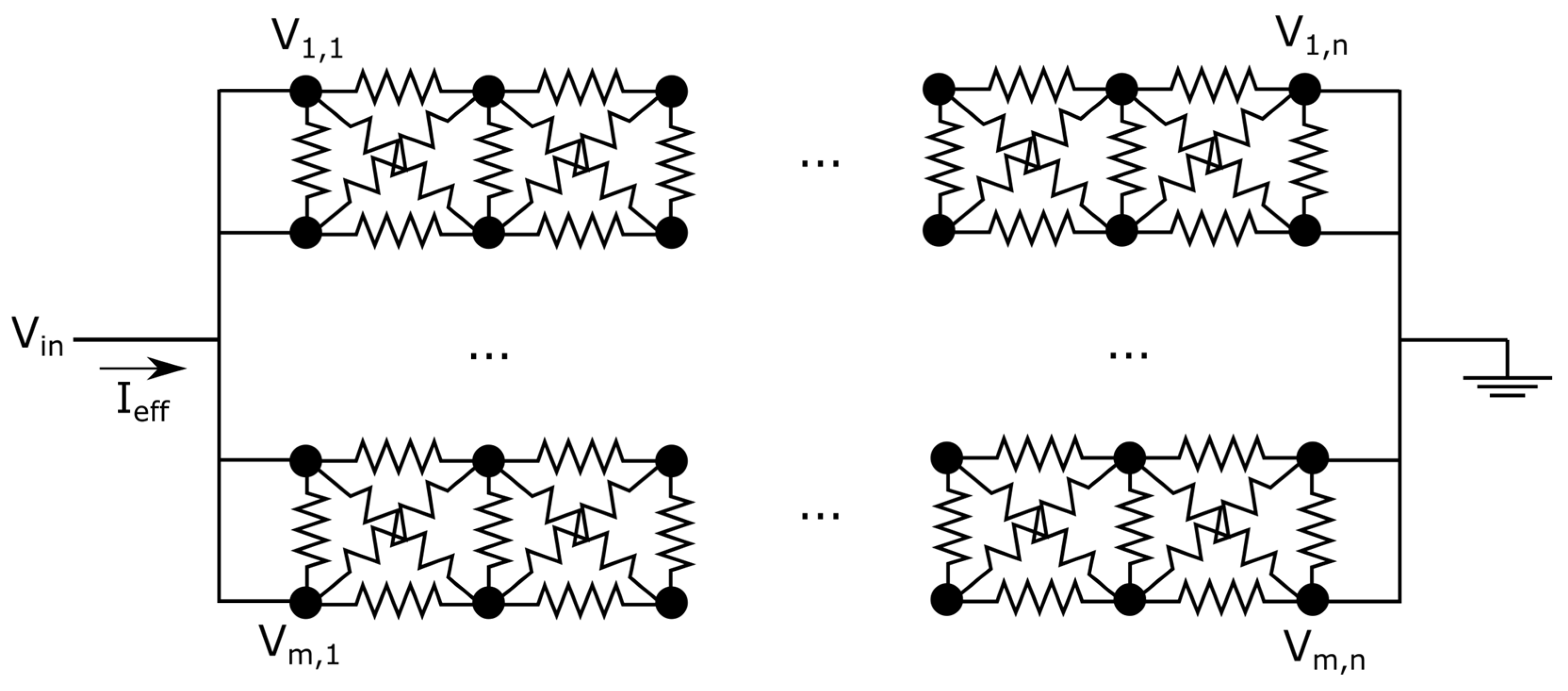
2. Methods: Simulation Setup

In order to fully understand and compare the validity of different percolation-type models, as applied to a conductive composite, a simulated electrical network was created. This network consists of a 500–500 grid of nodes, with the connections between nodes being assigned varying resistor values. The nodes represent conductive particles (assumed to have approximately infinite conductivity, compared with that of the tunneling gaps between them), and the resistors represent the tunneling gaps. Various topologies are possible to represent the lattice on which the nodes and resistors are assembled—such as a square or triangular lattice. In the physical nano-composite system, high aspect ratio fibers enable the formation of many connections per fiber that result in connected pathways even at low volume fractions, associated with a low percolation threshold. For example, a typical fiber filler 0.5 mm long and 50–60 μm sized clusters of nanoparticles [27] would potentially result in the number of connections to each fiber being approximately 8. Hence, the lattice used in simulations should have a high number of connections between nodes to approximate the behavior of the sensors. An eight-neighbor network was chosen, in order to meet this requirement of high connectivity and low percolation threshold.
The percolation threshold for a 2D lattice is often approximated by determining the fraction of conducting ‘bonds’ (or junctions) that results in an average of two being connected to each node (i.e., resulting in an ‘in’ and an ‘out’ path crossing the average node) [14]. Hence, a square lattice (4 bonds per node, with an average of 2 required to be conducting) has a percolation threshold of 0.5; a triangular lattice (6 bonds per node) has a threshold of close to 1/3 and the proposed lattice (8 bonds per node) has a threshold of close to 0.25. A schematic of a sample portion of the proposed network is shown in Figure 5.
In order to analyze the effective conductance across such a network, the entire left edge of the network is set at a constant non-zero voltage, and the entire right edge of the network is set at zero voltage. The effective conductance of the network is determined by numerical analysis. Kirchoff’s current law is applied at each internal node of the network, which states that the net current entering and leaving a junction must be the same. Ohm’s law is applied along each branch of the network, in the form of V G = I , where V is voltage, G conductance, and I the current. Using these two laws, equations for current at each branch of the junction can be written in terms of the voltages of the surrounding nodes and the conductance’s of the branches, leading to the construction of M*(N − 2) equations with M*(N − 2) unknowns. These equations can be rearranged into matrix form, and solved simultaneously to give the voltage at each node of the network.
The effective current through the network is determined by finding the current between the first two rows of the matrix, as this net current will remain constant throughout the network. The expression for this effective current is given by the equation:
I e f f = i = 1 m ( V i , 1 V i , 2 ) G i , 2 , ( i , 2 ) + i = 1 m 1 ( V i , 1 V i + 1,2 ) G i , 2 , ( i + 1,2 ) + i = 2 m ( V i , 1 V i 1,2 ) G i , 2 , ( i 1,2 )
The effective conductance of the network, G e f f , is determined by again applying Ohm’s law in the form of G e f f = I e f f / V s o u r c e , where V s o u r c e represents the source voltage applied to one end of the matrix and I e f f represents the current flowing through the network.
The value for effective conductance depends both on the connections of the network and the values of the individual resistances. If the network were made up of all resistors of equal value, the resulting conductance of the network would be a scaled value of the individual resistance. For an M × N network as used in this paper, there are 3*M − 2 resistors in parallel, and N − 1 resistors in series. The relationship between the conductance of the network of the individual resistors is given by the following:
G n o r m = G r e s i s t o r 3 M 2 N 1
where G r e s i s t o r is the conductance of an individual resistor, and G n o r m is the effective resistance of the entire network. For large networks this expression approaches G n o r m = 3 G r e s i s t o r . We scale our results by this constant value in order to facilitate comparison to the component resistor values.

3. Results

This study compares the simulated behavior of a resistor network using the multi-state percolation theory for a network of resistors representing tunneling gaps in a nano-composite. We present results for the following scenarios:
  • Conductance vs. volume fraction for a binary percolation case, to establish model parameters.
  • Conductance vs. volume fraction for a distribution of gaps between filler particles, using multi-state theory (MCEM).
  • Conductance vs. strain for a simple strain vs. gap distribution model using multi-state theory.
  • Conductance vs. strain for a more realistic strain vs. gap distribution model using multi-state theory.

3.1. Conductance vs. Volume Franction—Binary Case

In order to apply the GEM and MCEM models to the sensor conductive network, the percolation threshold and the values of the scaling exponents (s and t in Equation (4)) must be determined. These are determined by modeling the simplest version of the network, with each resistor in the lattice taking one of only two possible conductance values, 1 Ω−1 or 106 Ω−1, with the number fraction, p , indicating the fraction of gaps of high conductance. These values are used both for the simulation, as well as for generating the model predictions using Equation (4). These numbers are somewhat representative of possible conductance values across gaps between conductive particles, with the high conductance correlating with a gap size given by the adsorbed layer thickness, and the low conductance indicating a significantly larger gap. In experimenting with resistor networks of different sizes, we found that the maximum change in effective conductance was under 5% when using a network of 200 × 200 resistors, vs. 300 × 300 resistors. For our experiments, we use a 200 × 200 resistor network for its lower computational time. An optimization was performed which varied s, t and the percolation threshold, with the objective of minimizing the following objective function:
E r r o r = i 100 σ i θ i σ i   2
where σ i is the resulting conductivity, and θ i is the ith value of conductance predicted by the GEM model. The results of the optimization routine are displayed in Table 1. The agreement of the GEM model and the simulation results using these optimized values are shown in Figure 6. These values are consistent with reported values for these exponents. The calculated values for the scaling exponents will be used for the remainder of simulations presented in this paper. The figure also demonstrates that the GEM method captures the behavior of two-component systems when there is high contrast between the two components. We note that the GEM theory is equivalent to the MCEM theory with only two divisions.
To better visualize the percolation effect, the voltage distribution across the network is plotted, both below the percolation threshold (p = 0.1) and near the percolation threshold (p = 0.25), as shown in Figure 7. Away from the percolation threshold, charge is moving across the network in a uniform matter, with voltage gradually decreasing. In contrast, near the percolation threshold, charge follows a percolating cluster of linked high conductance branches, often leading to large contrast in voltage between neighbors.
In realistic silicone-nickel nano-composites, it is unlikely that gaps between conductive particles take binary values (conducting or non-conducting) as assumed above. While gaps above a few nanometers may all be assumed to be non-conducting, smaller (conducting) gaps are likely to have a range of sizes, and an associated distribution of conductance values given by Equation (1).

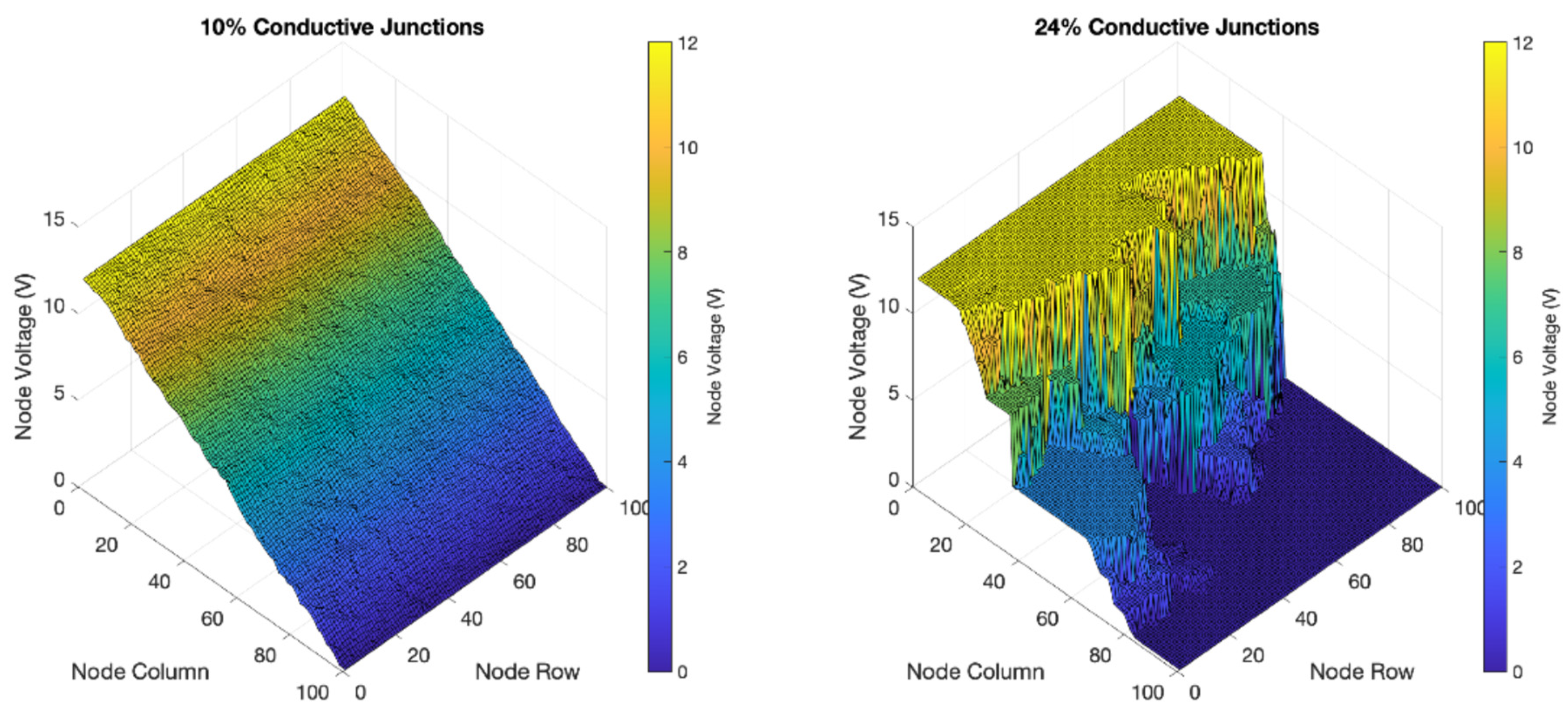
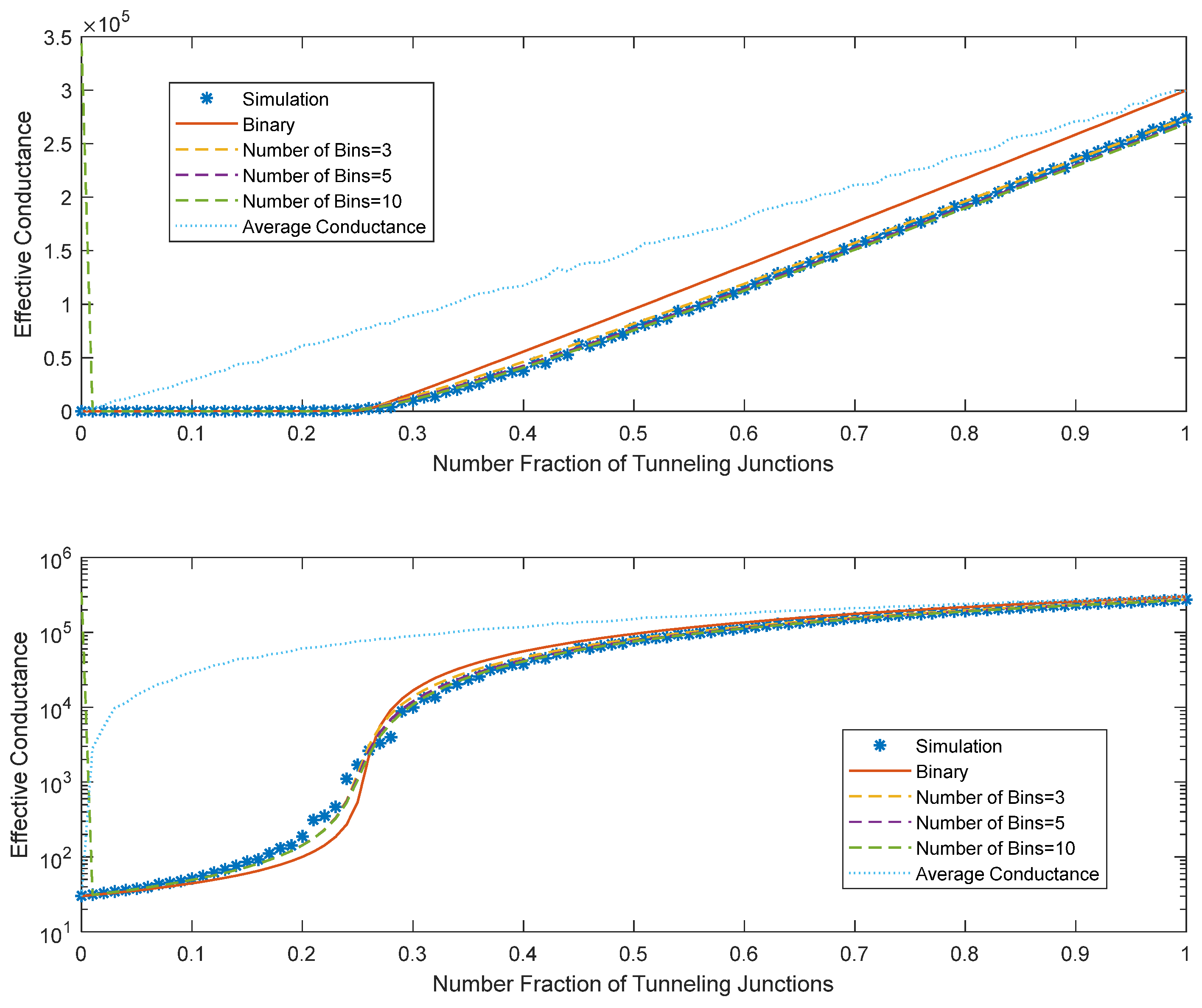
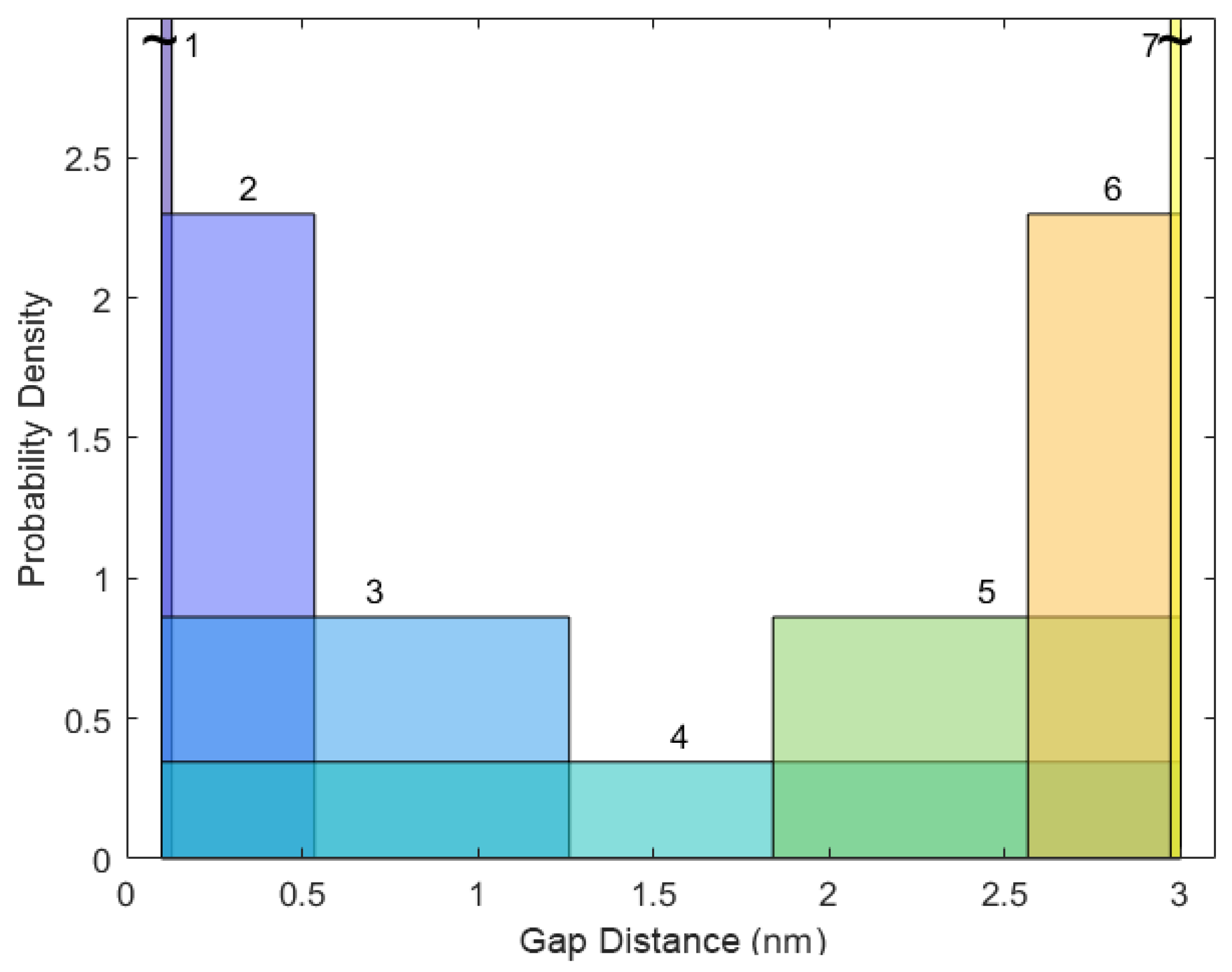
3.2. Conductance vs. Volume Franction—Uniform Gap Distribution

In this scenario, it is assumed that the volume fraction of conductive material is varied, and that the resultant conductance is controlled by a distribution of tunneling (conducting) gaps, with the number of conducting gaps being proportional to the volume fraction of conductive filler. For the initial case, the distribution of conducting gaps is represented by a uniform distribution of gap sizes, with a lower bound of 1 nm and an upper bound of 2 nm. Figure 8 compares the effective conductance of the network as the number fraction of junctions is varied from 0 to 1. Two models are compared with the random resistor network modeled in Figure 8: the usual binary version of the GEM model, where conducting gaps are all assigned a single value of conductance that is the average value for the assumed distribution, and a multi-state model, where the distribution is divided into N bins, with average conductance calculated from Equation (4).
It can be immediately seen that the binary model is significantly less accurate than the multi-state model. The multi-state method captures the transition from subcritical to supercritical behavior in the region of the percolation threshold (number fraction ~0.25), compared with a binary model. With an increasing number of bins in the multicomponent model, the accuracy increases relative to the random resistor network results, although there appears to be diminishing returns as more bins are added.

3.3. Conductance vs. Strain—Simple Gap Evolution Assumption

We now examine a case where the distribution of gap sizes within a composite undergoes a continuous change, as opposed to a discrete change, between distributions. When a nano-composite is used as a sensor, the distribution of gaps changes continuously as the device is stretched. In the classical percolation view, gaps switch discretely from a low to a high conductance value as the volume fraction of high conductance values varies continuously. Mathematically, this means the distribution of gap conductance is defined in terms of two delta functions, one at a high value of conductance, and the other at a low value. An assumption of a discrete transition of gap sizes between the two values that associate with these conductance levels is not consistent with continuous changes in gap size with strain. However, a potential continuous transition between the same endpoints involves a case in which a uniform distribution linearly moves its mean from the low value to the high value. The width of the distribution is set so as to always include either the high or low limit of the distribution. A few stages of the evolution of this distribution are shown in Figure 9.
The effective conductance for the simulated network and the predictions made by the binary and multi-state percolation equations are shown in Figure 10. We show the results with 2, 5, 10, and 20 bins. The case of two bins is equivalent to the binary conduction case. We also show the average conductance of the gaps in the network in Figure 10, which illustrates that this change cannot be modeled by a simple effective medium theory where the network behaves like the average gap.
For the assumed evolution of gap distributions, the conductance changes relatively gradually (on a logarithmic scale)—as opposed to displaying a sharper change at the percolation threshold. The binary (i.e., typical) percolation model does not reflect the behavior well. However, the multi-state percolation approach still captures the behavior of the network, even if the percolation effect is not dramatic. This ability to capture the behavior of both percolative and non-percolative systems is a valuable advantage of this technique.

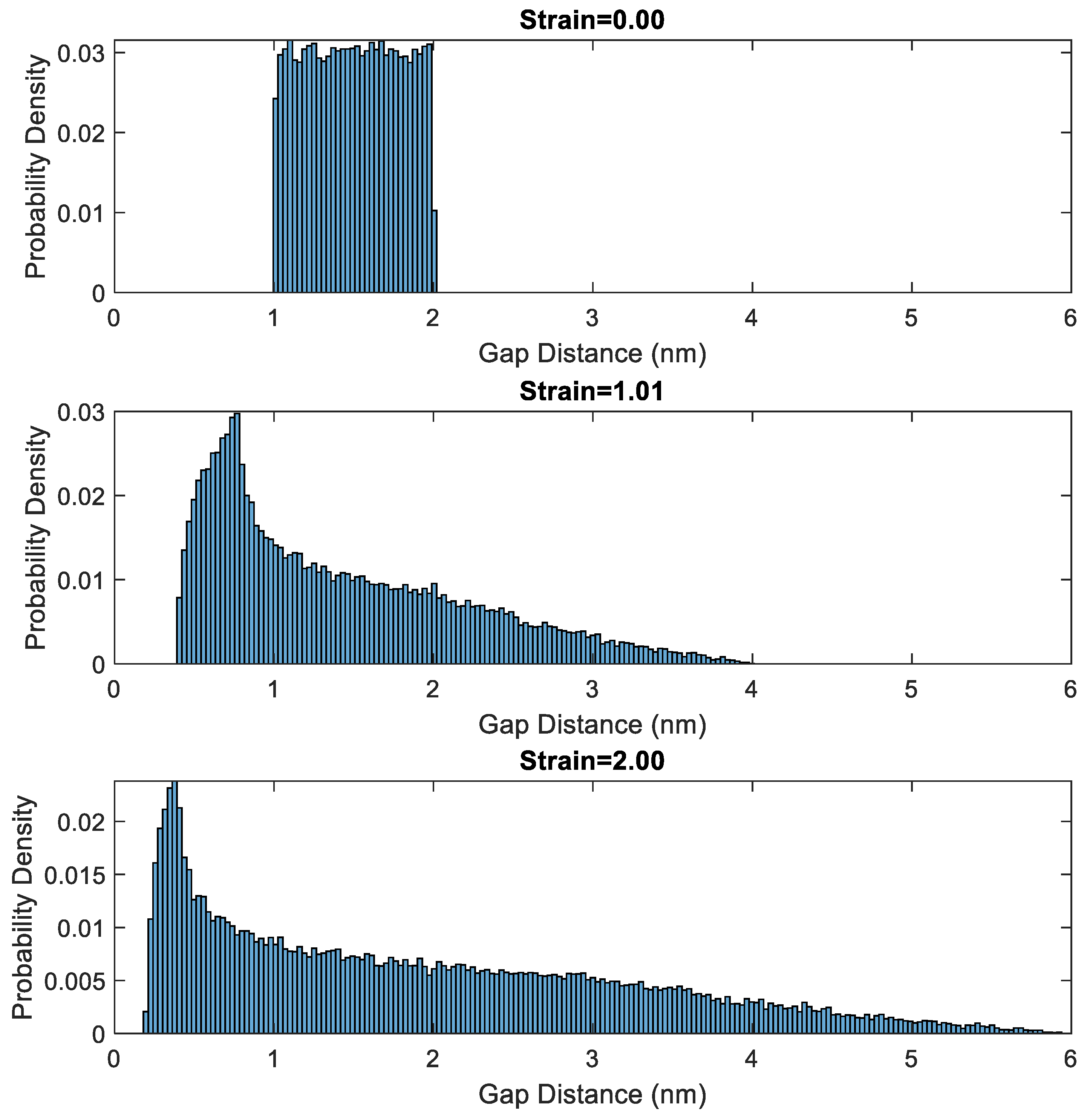
3.4. Conductance vs. Strain—Gaps Evolve According to Poisson Strain

A more realistic evolution of gap sizes in the nano-composite borrows from past work that proposed that gaps between conductive particles would evolve via a simple Poisson relationship [11]; as the sensor is stretched in one direction, contraction occurs in the other two orthogonal directions. Each gap is randomly assigned an orientation from 0 to 90 degrees in both the horizontal ϕ and vertical ( θ ) direction, such that the vector defining the gap is as follows:
r = d sin θ cos ϕ sin θ sin ϕ cos θ
where d is the gap distance When the material experiences a strain ϵ , the gaps evolve as follows:
r = 1 + ϵ 0 0 0 1 ν ϵ 0 0 0 1 ν ϵ r
where ν is Poisson’s ratio of the material. Gaps are assumed to be oriented randomly, with the result that under uniaxial strain approximately 1/3 of the gaps will increase in size, while 2/3 will decrease. While not capturing reality perfectly, as discussed in [11,12], this allows a reasonable estimate of gap changes with strain to be developed. Figure 11 shows the evolution of an initially uniform probability density function of gap sizes (assumed to range from 2 to 3 nm); the gap size distribution is illustrated for the initial unstrained material, and at 2 higher levels of uniaxial tensile strain where ν = 0.49 .
The resultant conductance across the network for this assumed Poisson dominated behavior was modeled using the random resistor network, and the results compared with predictions from the MCEM model, with different numbers of states, N; N = 2 represents standard binary percolation theory. The results are shown in Figure 12. For the multicomponent theory, the gap sizes were divided into evenly sized bins from 0 to 6 nm, with the effective conductance of each bin being the conductance of the average gap size for that bin.
Figure 12 indicates that there is no sharp percolation threshold where the conductance transitions from low to high values for this assumed evolution in conductive gaps. Presumably this results in very poor predictions by a typical percolation model (N = 2). As a multi-state model with more states is employed, the model converges on the random network simulation results. However, close to 20 states are required in the model for the results to be accurate. No doubt, other assumptions could be made (such as relating to alignment of fibers, or the initial distribution of gaps) that would lead to a more traditional percolative type transition from a non-conductive to a conductive network.
The outcome of this study demonstrates that if a percolation model with more than two states is employed (i.e., the MCEM model), it can be used for both traditional cases of clearly percolative behavior (such as modeling the relationship between number fraction of conductive gaps and sample conductance), as well cases that are not as clearly percolative in nature (such as the relationship between strain and conductance in high-elongation sensors).

4. Conclusions

This study considered the application of percolation-type models to piezoresistive composite sensors for two different situations: changes in conductivity due to change in volume fraction of conductive particles, and changes in conductivity due to changes in distribution of conductive gaps throughout the network when the sensor is strained.
The first case considered how the sample conductance changed with volume fraction of conductive filler. This volume fraction was assumed to correlate with the number fraction of conductive gaps in the network. Two-state percolation models were shown to capture the resulting electrical properties reasonably well. However, we found that if the conductivity of the conductive gaps varies widely (i.e., some nano-scale conducting gaps between conductive filler particles have much higher conductivity than others, as might realistically be the case for conductive composites), a multi-state percolation model with 10 to 20 divisions captures the behavior better than a simple binary model.
The second case considered was the relationship between sample conductance and the level of applied deformation, where the deformation modifies the size distribution of conductive gaps between filler particles. It was shown that the resultant change in conductance of the material is not well captured by a binary percolation model; the transition from low to high conductance is more gradual than is typically observed in percolative systems. Instead, a multi-state percolation model results in an accurate reflection of the expected behavior once the number of assumed states reaches between 10 and 20 divisions.
In summary, a multi-state model should be used to capture electrical response of composite materials with conductive filler particles. The multi-state model accurately captures network behavior when local properties of the electrical network can be assumed to be discrete (i.e., when conductivity at a given node in the network can be assumed to be approximately ‘on’ or ‘off’), or for cases where the changes in local conductivity are more continuous, as when the material undergoes strain.

Author Contributions

Conceptualization, N.S.U. and D.T.F.; methodology, N.S.U. and D.T.F.; data acquisition, D.T.F., A.E.B. and U.H.M.; analysis, N.S.U. and E.V.W.; investigation, N.S.U.; data curation, N.S.U.; writing—original draft preparation, N.S.U. and D.T.F.; writing—review and editing, N.S.U., E.V.W., D.T.F., A.E.B. and U.H.M.; project administration, D.T.F.; funding acquisition, A.E.B., D.T.F., N.S.U. and U.H.M. All authors have read and agreed to the published version of the manuscript.

Funding

This work was completed under NIH grant UH3AR076723, and NSF grant CMMI-1235365 with associated REU supplements. N.U. was also supported by NSF grant CBET-2344766.

Data Availability Statement

The original contributions presented in this study are included in the article. Further inquiries can be directed to the corresponding author.

Conflicts of Interest

The authors declare no conflicts of interest.

Abbreviations

The following abbreviations are used in this manuscript:
MCEMMulticomponent effective medium
GEMGeneral effective medium

References

  1. Pandey, G.; Biswas, A. Estimating Electrical Conductivity of multi-scale composites with conductive nanoparticles using bidirectional time marching percolation network mapping. Comput. Mater. Sci. 2014, 89, 8. [Google Scholar] [CrossRef]
  2. Gou, J.; Tang, Y.; Liang, F.; Zhao, Z.; Firsich, D.; Fielding, J. Carbon nanofiber paper for lightning strike protection of composite materials. Compos. Part B Eng. 2010, 41, 6. [Google Scholar] [CrossRef]
  3. Al-Saleh, M.H.; Sundararaj, U. A review of vapor grown carbon nanofiber/polymer conductive composites. Carbon 2009, 47, 20. [Google Scholar] [CrossRef]
  4. Kang, I.; Heung, Y.Y.; Kim, J.H.; Lee, J.W.; Gollapudi, R.; Subramaniam, S.; Narasimhadevara, S.; Hurd, D.; Kirikera, G.R.; Shanov, V.; et al. Introduction to carbon nanotube and nanofiber smart materials. Compos. Part B Eng. 2006, 37, 12. [Google Scholar] [CrossRef]
  5. Carney, A.; Niezrecki, C.; Buaka, P.; Chen, J.; Niemi, E. High Strain and Deformation Measurements using Imagin and Smart Material Sensors. In Proceedings of Sensors and Smart Structures Technologies for Civil, Mechanical, and Aerospace Systems; SPIE: Bellingham, WA, USA, 2007; p. 652933. [Google Scholar] [CrossRef]
  6. Nankali, M.; Nouri, N.M.; Navidbakhsh, M.; Malek, N.G.; Amindehghan, M.A.; Shahtoori, A.M.; Karimi, M.; Amjadi, M. Highly stretchable and sensitive strain sensors based on carbon nanotube–elastomer nanocomposites: The effect of environmental factors on strain sensing performance. J. Mater. Chem. C 2020, 8, 6185–6195. [Google Scholar] [CrossRef]
  7. Amjadi, M.; Kyung, K.-U.; Park, I.; Sitti, M. Stretchable, Skin-Mountable, and Wearable Strain Sensors and Their Potential Applications: A Review. Adv. Funct. Mater. 2016, 26, 1678–1698. [Google Scholar] [CrossRef]
  8. Han, S.; Zhang, X.; Wang, P.; Dai, J.; Guo, G.; Meng, Q.; Ma, J. Mechanically robust, highly sensitive and superior cycling performance nanocomposite strain sensors using 3-nm thick graphene platelets. Polym. Test. 2021, 98, 107178. [Google Scholar] [CrossRef]
  9. Zhang, Y.; Haghighi, P.D.; Burstein, F.; Yap, L.W.; Cheng, W.; Yao, L.; Cicuttini, F. Electronic skin wearable sensors for detecting lumbar–pelvic movements. Sensors 2020, 20, 1510. [Google Scholar] [CrossRef]
  10. Taya, M.; Kim, W.J.; Ono, K. Piezoresistivity of a short fiber/elastomer matrix composite. Mech. Mater. 1998, 28, 53–59. [Google Scholar] [CrossRef]
  11. Johnson, O.; Gardner, C.; Mara, N.; Dattelbaum, A.; Kaschner, G.; Mason, T.; Fullwood, D. Multi-scale Model for the Extreme Piezoresistivity in Silicone/Nickel Nanostrand/Nickel Coated Carbon Fiber Nanocomposites. MetTransA 2011, 42, 3898–3906. [Google Scholar]
  12. Clayton, M.F.; Bilodeau, R.A.; Bowden, A.E.; Fullwood, D.T. Nanoparticle orientation distribution analysis and design for polymeric piezoresistive sensors. Sens. Actuators A 2020, 303, 111851. [Google Scholar] [CrossRef]
  13. Wonnacott, A.M.; Bowden, A.E.; Mitchell, U.H.; Fullwood, D.T. Analyzing and Modeling the Dynamic Electrical Characteristics of Nanocomposite Large-Range Strain Gauges. Sensors 2024, 24, 8192. [Google Scholar] [CrossRef] [PubMed]
  14. Stauffer, D.; Aharony, A. Introduction to Percolation Theory, 2nd ed.; Taylor and Francis: Bristol, PA, USA, 1992. [Google Scholar]
  15. Torquato, S. Random Heterogeneous Materials; Springer: New York, NY, USA, 2002. [Google Scholar]
  16. Grimmett, G. Percolation, 2nd ed.; Springer: Berlin/Heidelberg, Germany, 1999; Volume 321. [Google Scholar]
  17. Chen, Y.; Schuh, C.A. Diffusion on grain boundary networks: Percolation theory and effective medium approximations. Acta Mater. 2006, 54, 4709–4720. [Google Scholar] [CrossRef]
  18. Koecher, M.; Yeager, J.; Park, T.; Mara, N.; Fullwood, D.; Hansen, N.; Colton, J.S. Characterization of Nickel Nanostrand Nanocomposites through Dielectric Spectroscopy and Nanoindentation. Polym. Eng. Sci. 2013, 53, 2666–2673. [Google Scholar] [CrossRef]
  19. Morozov, I.; Lauke, B.; Heinrich, G. A new structural model of carbon black framework in rubbers. Comput. Mater. Sci. 2010, 47, 8. [Google Scholar] [CrossRef]
  20. Toker, D.; Azulay, D.; Shimoni, N.; Balberg, I.; Millo, O. Tunneling and percolation in metal-insulator composite materials. Phys. Rev. B 2003, 68, 041403. [Google Scholar] [CrossRef]
  21. Wang, L.; Xu, C.; Li, Y. Piezoresistive repsonse to changes in contributive tunneling film network of carbon nanotube/silicone rubber composite under muli-load/unload. Sens. Actuators A 2013, 189, 45–54. [Google Scholar] [CrossRef]
  22. Ambrosetti, G.; Grimaldi, C.; Balberg, I.; Maider, T.; Danani, A.; Ryser, P. Solution of the tunneling-percolation problem in the nanocomposite regime. Phys. Rev. B 2010, 81, 155434. [Google Scholar] [CrossRef]
  23. Hu, N.; Karube, Y.; Yan, C.; Masuda, Z.; Fukunaga, H. Tunneling Efffect in a Polymer/Carbon Nanotube Nanocomposite Strain Sensor. Acta Mater. 2008, 56, 2929–2936. [Google Scholar] [CrossRef]
  24. Fritzsche, J.; Lorenz, H.; Kluppel, M. CNT Based Elastomer-Hybrid-Nanocomposites with Promising Mechanical and Electrical Properties. Macromol. Mater. Eng. 2009, 294, 551–560. [Google Scholar] [CrossRef]
  25. Sahimi, M. Critical Exponent of Percolation Conductivity by Finite-Size Scaling. J. Phys. C Solid State Phys. 1983, 16, L521–L527. [Google Scholar] [CrossRef]
  26. Dalafi, A.; Dalafi, D.; Hadi, I.; Ebrahimi, S.; Jafari, M. Computer Study of critical exponents in two-dimensional systems of circular and sticklike nanoparticles. Comput. Mater. Sci. 2013, 68, 12. [Google Scholar] [CrossRef]
  27. Hansen, N.; Adams, D.O.; Fullwood, D.T. Evaluation and Development of Percolation Models for Electrical Conductivity in Nickel Nanostrand Polymer Composites. J. Polym. Eng. Sci. 2015, 55, 549–557. [Google Scholar] [CrossRef]
Figure 1. Nickel nano-strands before being embedded in an insulating polymer.
Jcs 09 00354 g001
Figure 2. Change in gap conductance with increasing gap size for a nickel/polymer combination that has a barrier height of 0.2802 eV. Note that conductance quickly approaches 0 as gap size increases.
Jcs 09 00354 g002
Figure 3. Schematic of an approximation of the conductance curve when using two bins with the GEM approach.
Jcs 09 00354 g003
Figure 4. Representation of the division of a continuous conductance curve into discrete values using the MCEM approach.
Jcs 09 00354 g004
Figure 5. Schematic of network studied; each non-edge node has eight connections.
Jcs 09 00354 g005
Figure 6. Comparison of simulation results and GEM Equations using the optimized values for the percolation threshold and the scaling exponents (Table 1).
Jcs 09 00354 g006
Figure 7. Voltage distribution throughout a network with number fraction of conductive junctions given by 0.1 and 0.24. The voltage distribution is smooth far from the percolation threshold (left) but jagged close to the percolation threshold (right).
Jcs 09 00354 g007
Figure 8. Performance of network conductance models, where the size of tunneling/conductive gaps are assigned to follow a uniform distribution All other gaps are assumed to be too large for tunneling to occur, and are assigned a constant very low conductance. The simulation results are calculated using the random resistor network, and assumed to be the ground truth; the number of bins in each MCEM model are given in the legend.
Jcs 09 00354 g008
Figure 9. Evolution in gap distribution from initial case (1: all gaps are 0.1 nm wide, represented by a delta function) to case 7 (all gaps are 3 nm wide) for the results presented in Figure 10 (colors are arbitrary, for easy visualization).
Jcs 09 00354 g009
Figure 10. Performance of various models vs. the random assumed ground truth simulation for the developing distribution case shown in Figure 9. The binary case assumes N = 2.
Jcs 09 00354 g010
Figure 11. Evolution of initial approximately uniform distribution of gap size (top figure) at two subsequent levels of strain (middle and bottom figures).
Jcs 09 00354 g011
Figure 12. Conductance at multiple levels of strain when the distribution of gap distance follows the development shown in Figure 11. With increasing numbers of divisions, the model more closely approximates the simulation results.
Jcs 09 00354 g012
Table 1. Optimized results for the proper value of the scaling exponents and the percolation threshold.
VariableOptimized Value
s0.7918
t1.0288
p c 0.255
Disclaimer/Publisher’s Note: The statements, opinions and data contained in all publications are solely those of the individual author(s) and contributor(s) and not of MDPI and/or the editor(s). MDPI and/or the editor(s) disclaim responsibility for any injury to people or property resulting from any ideas, methods, instructions or products referred to in the content.

