


Preparation and Photoelectric Properties of Nanostructured Native Oxide of Gallium Monoselenide with Applications in Gas Sensors


 ,
,  and
and 
Abstract
1. Introduction
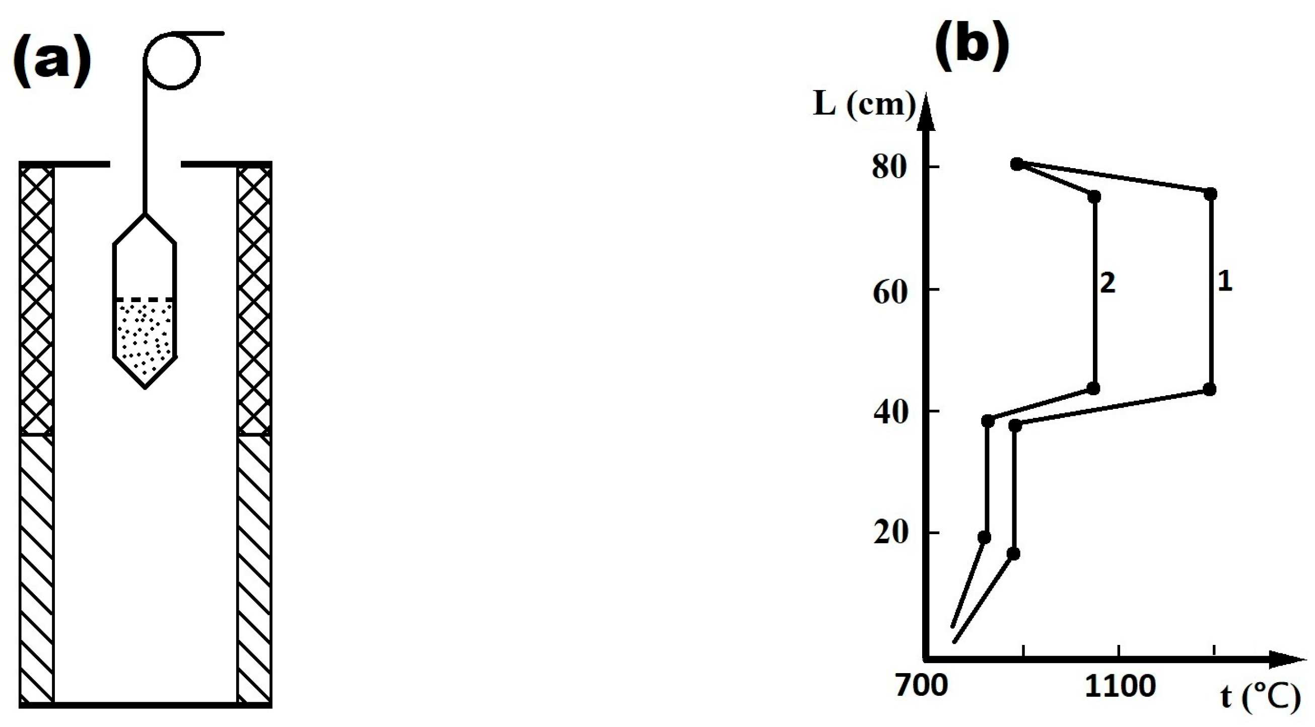
2. Materials and Methods
3. Results
3.1. Crystal Structure and Material Composition
Raman Spectra
3.2. Surface Morphology of Ga2Se3–Ga2O3 Composite Layers and β–Ga2O3
3.3. Absorption Band Edge Analysis
3.4. Photoresponse of Photoresistors Based on Untreated and Air-Heated Single Crystalline GaSe Plates
4. Conclusions
Author Contributions
Funding
Data Availability Statement
Acknowledgments
Conflicts of Interest
References
- Fritz, H. Structural Chemistry of Layer-Type Phases; Springer Science & Business Media: Dordrecht, The Netherlands, 1976. [Google Scholar]
- Schlueter, M. The electronic structure of GaSe. Nuovo Cim. B 1973, 13, 313–360. [Google Scholar] [CrossRef]
- Plucinski, L.; Johnson, R.L.; Kowalski, B.J.; Kopalko, K.; Orlowski, B.A.; Kovalyuk, Z.D.; Lashkarev, G.V. Electronic band structure of GaSe (0001): Angle-resolved photoemission and ab initio theory. Phy. Rev. B 2003, 68, 125304. [Google Scholar] [CrossRef]
- Wieting, T.J.; Verble, J.L. Interlayer bonding and the latratament termicice vibrations of β–GaSe. Phy. Rev. B 1972, 5, 1473–1479. [Google Scholar] [CrossRef]
- Jellinek, F.; Hahn, H. Zur polytypie des galliummonoselenids, gase. Z. Naturforsch. B 1961, 16, 713–715. [Google Scholar] [CrossRef]
- Lang, O.; Schlaf, R.; Tomm, Y.; Pettenkofer, C.; Jaegermann, W. Single crystalline GaSe/WSe2 heterointerfaces grown by van der Waals epitaxy. I. Growth conditions. J. Appl. Phys. 1994, 75, 7805–7813. [Google Scholar]
- Lei, S.; Ge, L.; Liu, Z.; Najmaei, S.; Shi, G.; You, G.; Lou, J.; Vajtai, R.; Ajayan, P.M. Synthesis and photoresponse of large GaSe atomic layers. Nano Lett. 2013, 13, 2777–2781. [Google Scholar] [CrossRef] [PubMed]
- Williams, R.H.; McEvoy, A.J. Electron emission studies from GaSe surfaces. J. Vac. Sci. Technol. 1972, 9, 867–870. [Google Scholar] [CrossRef]
- Le Toullec, R.; Balkanski, M.; Besson, J.M.; Kuhn, A. Optical absorption edge of a new GaSe polytype. Phys. Lett. A 1975, 55, 245–246. [Google Scholar] [CrossRef]
- Gan, X.-T.; Zhao, C.-Y.; Hu, S.-Q.; Wang, T.; Song, Y.; Li, J.; Zhao, Q.-H.; Jie, W.-Q.; Zhao, J.-L. Microwatratament termics continuous-wave pumped second harmonic generation in few-and mono-layer GaSe. Light Sci. Appl. 2018, 7, 17126. [Google Scholar] [CrossRef]
- Afaneh, T.; Fryer, A.; Xin, Y.; Hyde, R.H.; Kapuruge, N.; Gutiérrez, H.R. Large-area growth and stability of monolayer gallium monochalcogenides for optoelectronic devices. ACS Appl. Nano Mater. 2020, 3, 7879–7887. [Google Scholar] [CrossRef]
- Drapak, S.I.; Gavrilyuk, S.V.; Kovalyuk, Z.D.; Litvin, O.S. Native oxide emerging of the cleavage surface of gallium selenide due to prolonged storage. Semiconductors 2008, 42, 414–421. [Google Scholar] [CrossRef]
- Beechem, T.; Kowalski, B.; Brumbach, M.; McDonald, A.E.; Spataru, C.D.; Howell, S.W.; Ohta, T.; Pask, J.A.; Kalugin, N. Oxidation of ultrathin GaSe. Appl. Phys. Lett. 2015, 107, 173103. [Google Scholar] [CrossRef]
- Filippo, E.; Siciliano, M.; Genga, A.; Micocci, G.; Tepore, A.; Siciliano, T. Single crystalline β–Ga2O3 nanowires synthesized by thermal oxidation of GaSe layer. Mater. Res. Bull. 2013, 48, 1741–1744. [Google Scholar] [CrossRef]
- Xue, W.; Faizan, M.; Na, G.; He, X.; Fu, Y.H.; Zhang, L. Discovery of new polymorphs of gallium oxides with particle swarm optimization-based structure searches. Adv. Electron. Mater. 2020, 6, 2000119. [Google Scholar]
- Masataka, H.; Shizuo, F. Gallium Oxide: Materials Properties, Crystal Growth, and Devices; Springer: Berlin/Heidelberg, Germany, 2020; Volume 293. [Google Scholar]
- Kanika, A.; Mukesh, K. Sputratament termicered-growth of high-temperature seed-layer assisted β–Ga2O3 thin film on silicon-substrate for cost-effective solar-blind photodetector application. ECS J. Solid State Sci. Technol. 2020, 9, 065013. [Google Scholar]
- Hyunsu, K.; Jin, C.; Park, S.; Lee, W.I.; Lee, C. Structure and luminescence properties of thermally nitrided Ga2O3 nanowires. Mater. Res. Bull. 2013, 48, 613–617. [Google Scholar]
- Tippins, H.H. Optical absorption and photoconductivity in the band edge of β−Ga2O3. Phys. Rev. 1965, 140, A316. [Google Scholar] [CrossRef]
- Berale, E.; Zapan, M. Organic Chemistry; Tehnica: Bucharest, Romania, 1977; p. 680. [Google Scholar]
- Washenfelder, R.A.; Wagner, N.L.; Dube, W.P.; Brown, S.S. Measurement of atmospheric ozone by cavity ring-down spectroscopy. Environ. Sci. Technol. 2011, 45, 2938–2944. [Google Scholar] [CrossRef]
- Sui, Y.; Liang, H.; Chen, Q.; Huo, W.; Du, X.; Mei, Z. Room-temperature ozone sensing capability of IGZO-decorated amorphous Ga2O3 films. ACS Appl. Mater. Interfaces 2020, 12, 8929–8934. [Google Scholar] [CrossRef]
- Garner, A.L.; St Croix, C.M.; Pitt, B.R.; Leikauf, G.D.; Ando, S.; Koide, K. Specific fluorogenic probes for ozone in biological and atmospheric samples. Nat. Chem. 2009, 1, 316–321. [Google Scholar] [CrossRef]
- Alema, F.; Hertog, B.; Osinsky, A.; Mukhopadhyay, P.; Toporkov, M.; Schoenfeld, W.V. Fast growth rate of epitaxial β–Ga2O3 by close coupled showerhead MOCVD. J. Cryst. Growth 2017, 475, 77–82. [Google Scholar] [CrossRef]
- Makeswaran, N.; Battu, A.K.; Deemer, E.; Ramana, C.V. Crystal growth and structure–property optimization of thermally annealed nanocrystalline Ga2O3 films. Cryst. Growth Des. 2020, 20, 2893–2903. [Google Scholar] [CrossRef]
- Galván, C.; Galván, M.; Arias-Cerón, J.S.; López-Luna, E.; Vilchis, H.; Sánchez-R, V.M. Structural and Raman studies of Ga2O3 obtained on GaAs substrate. Mater. Sci. Semicond. Process. 2016, 41, 513–518. [Google Scholar] [CrossRef]
- Lübbers, D.; Leute, V. The crystal structure of β-Ga2Se3. J. Solid State Chem. 1982, 43, 339–345. [Google Scholar] [CrossRef]
- Kathryn, G.; (Kees) de Groot, C.H.; Gurnani, C.; Hector, A.L.; Huang, R.; Jura, M.; Levason, W.; Reid, G. Telluroether and selenoether complexes as single source reagents for low pressure chemical vapor deposition of crystalline Ga2Te3 and Ga2Se3 thin films. Chem. Mater. 2013, 25, 1829–1836. [Google Scholar]
- Kanaya, K.; Okayama, S. Penetration and energy-loss theory of electrons in solid targets. J. Phys. D Appl. Phys. 1972, 5, 43–58. [Google Scholar] [CrossRef]
- Dai, L.; Chen, X.; Zhang, X.N.; Jin, A.Z.; Zhou, T.; Hu, B.Q.; Zhang, Z. Growth and optical characterization of Ga2O3 nanobelts and nanosheets. J. Appl. Phys. 2002, 92, 1062–1064. [Google Scholar] [CrossRef]
- Weng, T.-F.; Ho, M.-S.; Chandrasekar, S.; Babu, B.; Chung, P.-F. VLS growth of pure and Au decorated β–Ga2O3 nanowires for room temperature CO gas sensor and resistive memory applications. Appl. Surf. Sci. 2020, 533, 147476. [Google Scholar] [CrossRef]
- Kojima, N.; Akira, Y.; Kiyoshi, T.; Tamotsu, O.; Makoto, K.; Koki, S. Photoinduced oxidation of epitaxial Ga2Se3 grown by molecular beam epitaxy. Jpn. J. Appl. Phys. 1993, 32, L887. [Google Scholar] [CrossRef]
- Ryota, I.; Masato, A.; Akiyo, O.; Yuma, K.; Yu, K.; Muneaki, Y.; Tetsuo, T.; Tomoko, Y. Photocatalytic activity of Ga2O3 supported on Al2O3 for water splitting and CO2 reduction. ACS Omega 2019, 4, 5451–5458. [Google Scholar]
- Guenter, W.; Baldini, M.; Gogova, D.; Schmidbauer, M.; Schewski, R.; Albrecht, M.; Galazka, Z.; Klimm, D.; Fornari, R. Homoepitaxial growth of β–Ga2O3 layers by metal-organic vapor phase epitaxy. Phys. Status Solidi A 2014, 211, 27–33. [Google Scholar]
- Navarro-Quezada, A.; Galazka, Z.; Alamé, S.; Skuridina, D.; Vogt, P.; Esser, N. Surface properties of annealed semiconducting β–Ga2O3 (1 0 0) single crystals for epitaxy. Appl. Surf. Sci. 2015, 349, 368–373. [Google Scholar] [CrossRef]
- Siciliano, T.; Tepore, M.; Genga, A.; Micocci, G.; Siciliano, M.; Tepore, A. Thermal oxidation of amorphous GaSe thin films. Vacuum 2013, 92, 65–69. [Google Scholar] [CrossRef]
- Balitskii, O.A.; Savchyn, V.P. Thermodynamic study of AIIIBVI compounds oxidation. Mater. Sci. Semicond. Process. 2004, 7, 55–58. [Google Scholar] [CrossRef]
- Jouanne, M.; Julien, C.; Balkanski, M. Polarization studies of polar phonons of InSe. Phys. Status Solidi B 1987, 144, K147–K150. [Google Scholar] [CrossRef]
- Bletskan, D.I.; Kabatsii, V.N.; Kranjčec, M. Photoelectric properties of ordered-vacancy Ga2Se3 single crystals. Inorg. Mater. 2010, 46, 1290–1295. [Google Scholar] [CrossRef]
- Zhengwei, C.; Wang, X.; Saito, K.; Tanaka, T.; Nishio, M.; Guo, Q. The impact of growth temperature on the structural and optical properties of catalyst-free β–Ga2O3 nanostructures. Mater. Res. Express 2016, 3, 025003. [Google Scholar]
- Chun, H.J.; Young, S.C.; Seung, Y.B.; Hee, W.S.; Su, J.H.; Jeunghee, P.; Hyunik, Y. Controlled structure of gallium oxide nanowires. J. Phys. Chem. B 2003, 107, 9042–9046. [Google Scholar] [CrossRef]
- Dohy, D.; Lucazeau, G.; Revcolevschi, A. Raman spectra and valence force field of single-crystalline β–Ga2O3. J. Solid State Chem. 1982, 45, 180–192. [Google Scholar] [CrossRef]
- Cai, K.F.; Shen, S.; Yan, C.; Bateman, S. Preparation, characterization and formation mechanism of gallium oxide nanowires. Curr. Appl. Phys. 2008, 8, 363–366. [Google Scholar] [CrossRef]
- Zhirko, Y.I.; Zharkov, I.P. Investigation of some mechanisms for formation of exciton absorption bands in layered semiconductor n–InSe and p–GaSe crystals. Semicond. Phys. Quantum Electron. Optoelectron. 2003, 6, 134–140. [Google Scholar] [CrossRef]
- Kuroda, T.; Yamauchi, Y.; Minami, F. Spin beats of anisotropic excitons in GaSe. J. Lumin. 2000, 87, 213–215. [Google Scholar] [CrossRef]
- Le Toullec, R.; Piccioli, N.; Chervin, J.C. Optical properties of the band-edge exciton in GaSe crystals at 10 K. Phys. Rev. B 1980, 22, 6162–6170. [Google Scholar] [CrossRef]
- Zalamai, V.V.; Syrbu, N.; Stamov, I.G.; Beril, I. Wannier–Mott excitons in GaSe single crystals. J. Opt. 2020, 22, 085402. [Google Scholar] [CrossRef]
- Mooser, E.; Schlüter, M. The band-gap excitons in gallium selenide. Il Nuovo Cimento B 1973, 18, 164–208. [Google Scholar] [CrossRef]
- Gauthier, M.; Polian, A.; Besson, J.M.; Chevy, A. Optical properties of gallium selenide under high pressure. Phys. Rev. B 1989, 40, 3837. [Google Scholar] [CrossRef] [PubMed]
- Takumi, M.; Koshio, Y.; Nagata, K. X-Ray, Raman and Photoluminescence Study of Vacancy Ordered β–Ga2Se3 under High Pressure. Phys. Status Solidi B 1999, 211, 123–129. [Google Scholar] [CrossRef]
- Yoon, C.-S.; Park, K.-H.; Kim, D.-T.; Park, T.-Y.; Jin, M.-S.; Oh, S.-K.; Kim, W.-T. Optical properties of Ga2Se3 and Ga2Se3: Co2+ single crystals. J. Phys. Chem. Solids 2001, 62, 1131–1137. [Google Scholar] [CrossRef]
- Springford, M. The luminescence characteristics of some group III-VI compounds. Proc. Phys. Soc. 1963, 82, 1020. [Google Scholar] [CrossRef]
- Okamoto, T.; Nobuaki, K.; Akira, Y.; Makoto, K.; Kiyoshi, T.; Yoshio, N.; Osamu, N. Optical anisotropy of vacancy-ordered Ga2Se3 grown by molecular beam epitaxy. Jpn. J. Appl. Phys. 1992, 31, L143. [Google Scholar] [CrossRef]
- Boldish, S.I.; White, W.B. Optical band gaps of selected ternary sulfide minerals. Am. Min. 1998, 83, 865–871. [Google Scholar] [CrossRef]
- Murphy, A.B. Modified Kubelka–Munk model for calculation of the reflectance of coatings with optically-rough surfaces. J. Phys. D Appl. Phys. 2006, 39, 3571. [Google Scholar] [CrossRef]
- Bizarro, M.; Rodil, S.E. Physicochemical characterization of photocatalytic materials. In Photocatalytic Semiconductors: Synthesis, Characterization, and Environmental Applications; Springer International Publishing: Cham, Switzerland, 2015; pp. 103–153. [Google Scholar]
- Varley, J.B.; Weber, J.R.; Janotti, A.; Van de Walle, C.G. Oxygen vacancies and donor impurities in β–Ga2O3. Appl. Phys. Lett. 2010, 97, 142106. [Google Scholar] [CrossRef]
- Du, X.; Zhao, L.; Caina, L.; Weiguang, W.; Mingxian, W.; Xianjin, F.; Hongdi, X.; Jin, M. Preparation and characterization of Sn–doped β–Ga2O3 homoepitaxial films by MOCVD. J. Mater. Sci. 2015, 50, 3252–3257. [Google Scholar] [CrossRef]
- Nieto-Caballero, F.G.; García-Salgado, G.; Díaz-Becerril, T.; Rosendo-Andrés, E.; Juárez-Santiesteban, H.; Gracia-Jiménez, M.; Tovar-Corona1, A.; Peña- Rosas, U.; Peña-Sierra, R. β–Ga2O3 Particles Formed of a Complex Organic by Electrolysis. Int. J. Electrochem. Sci. 2015, 10, 9742–9750. [Google Scholar] [CrossRef]
- Razbirin, B.; Mushinskii, V.; Karaman, M.; Starukhin, A.; Gamarts, E. Optical alignment of excitons in GaSe. Izv. Akad. Nauk SSSR Ser. Fiz. 1976, 40, 1872–1875. [Google Scholar]
- Abdal-Rahman, M.; El Shaikh, H.A. Photoelectric properties of single crystals. J. Phys. D Appl. Phys. 1996, 29, 889. [Google Scholar] [CrossRef]
- Sasaki, K.; Masataka, H.; Akito, K.; Takekazu, M.; Shigenobu, Y. MBE grown Ga2O3 and its power device applications. J. Cryst. Growth 2013, 378, 591–595. [Google Scholar] [CrossRef]
- Orita, M.; Hiromichi, O.; Masahiro, H.; Hideo, H. Deep-ultraviolet transparent conductive β–Ga2O3 thin films. Appl. Phys. Lett. 2000, 77, 4166–4168. [Google Scholar] [CrossRef]
- Zhang, F.; Li, H.; Guo, Q. Structural and Electrical Properties of Ga2O3 Films Deposited under Different Atmospheres by Pulsed Laser Deposition. J. Electron. Mater. 2018, 47, 6635–6640. [Google Scholar] [CrossRef]
- Wong, M.H.; Lin, C.-H.; Akito, K.; Shigenobu, Y.; Hisashi, M.; Yoshinao, K.; Masataka, H. Acceptor doping of β–Ga2O3 by Mg and N ion implantations. Appl. Phys. Lett. 2018, 113, 102103. [Google Scholar] [CrossRef]
- Gao, H.; Junying, Z.; Min, L.; Kejia, L.; Dong, G.; Yue, Z. Evaluating the electric property of different crystal faces and enhancing the Raman scattering of Cu2O microcrystal by depositing Ag on the surface. Curr. Appl. Phys. 2013, 13, 935–939. [Google Scholar] [CrossRef]
- Shannon, R.D. Revised Effective Ionic Radii and Systematic Studies of Interatomic Distances in Halides and Chalcogenides. Acta Crystallogr. 1976, A32, 751–767. [Google Scholar] [CrossRef]
- Gailin, G.; Li, G. Microstructure and properties of Cu-doped β–Ga2O3 rod prepared with liquid metallic gallium. J. Eur. Ceram. Soc. 2025, 45, 116916. [Google Scholar]
- Babu, A.; Rao, N.M. Effect of copper substitution on the structural, optical, and magnetic properties of β–Ga2O3 powders. Appl. Phys. A 2025, 131, 172. [Google Scholar] [CrossRef]
- Neal, A.T.; Mou, S.; Rafique, S.; Zhao, H.; Ahmadi, E.; Speck, J.S.; Stevens, K.T.; Blevins, J.D.; Thomson, D.B.; Moser, N.; et al. Donors and deep acceptors in β–Ga2O3. Appl. Phys. Lett. 2018, 113, 062101. [Google Scholar] [CrossRef]
- Du, J.; Jie, X.; Chen, G.; Hao, L.; Pengyu, L.; Huiying, H.; Jingjing, D.; Zhiyuan, Z.; Hua, G. Highly sensitive and ultrafast deep UV photodetector based on a β–Ga2O3 nanowire network grown by CVD. J. Phys. D Appl. Phys. 2016, 49, 425105. [Google Scholar] [CrossRef]
- Sui, Y.; Huili, L.; Wenxing, H.; Yan, W.; Zengxia, M. A flexible and transparent β–Ga2O3 solar-blind ultraviolet photodetector on mica. J. Phys. D Appl. Phys. 2020, 53, 504001. [Google Scholar] [CrossRef]
- Veaceslav, S.; Caraman, M.; Qiu, H.; Tjardts, T.; Sereacov, A.; Aktas, C.; Adelung, R.; Lupan, O. Photodetector Based on β–Ga2O3 Nanowires on GaSxSe1-X Solid Solution Substrate. In International Conference on Nanotechnologies and Biomedical Engineering; Springer: Berlin/Heidelberg, Germany, 2023. [Google Scholar]
- Wang, S.; Hanlin, S.; Zhe, W.; Xiaohui, Z.; Goran, U.; Daoyou, G.; Jingqin, S.; Peigang, L.; Aiping, L.; Chaorong, L.; et al. In situ synthesis of monoclinic β–Ga2O3 nanowires on flexible substrate and solar-blind photodetector. J. Alloys Compd. 2019, 787, 133–139. [Google Scholar] [CrossRef]
- Cui, S.-J.; Mei, Z.-X.; Hou, Y.-N.; Chen, Q.-S.; Liang, H.-L.; Zhang, Y.-H.; Huo, W.-X.; Du, X.-L. Enhanced photoresponse performance in Ga/Ga2O3 nanocomposite solar-blind ultraviolet photodetectors. Chin. Phys. B 2018, 27, 067301. [Google Scholar] [CrossRef]
- Wang, Q.; Jian, C.; Pan, H.; Mingkai, L.; Yinmei, L.; Homewood, K.P.; Gang, C.; Hong, C.; Yunbin, H. Influence of growth temperature on the characteristics of β–Ga2O3 epitaxial films and related solar-blind photodetectors. Appl. Sur. Sci. 2019, 489, 101–109. [Google Scholar] [CrossRef]
- Jangir, R.; Tapas, G.; Pragya, T.; Porwal, S.; Himanshu, S.; Rai, S.K.; Khattak, B.Q.; Oak, S.M. Synthesis and characterization of β–Ga2O3 nanostructures grown on GaAs substrates. Appl. Sur. Sci. 2011, 257, 9323–9328. [Google Scholar] [CrossRef]
- Zhou, C.; Liu, K.; Xing, C.; Jiaheng, F.; Jialin, Y.; Zhenzhong, Z.; Lei, L.; Yang, X.; Dezhen, S. Performance improvement of amorphous Ga2O3 ultraviolet photodetector by annealing under oxygen atmosphere. J. Alloys Compd. 2020, 840, 155585. [Google Scholar] [CrossRef]
- Seeger, K. Semiconductor Physics; Springer: Berlin, Germany, 1973. [Google Scholar]
- Qu, Y.; Wu, Z.; Ai, M.; Guo, D.; An, Y.; Yang, H.; Li, L.; Tang, W. Enhanced Ga2O3/SiC ultraviolet photodetector with graphene top electrodes. J. Alloys Compd. 2016, 680, 247–251. [Google Scholar] [CrossRef]
- Yoon, Y.; Kim, S.; Lee, I.G.; Cho, B.J.; Hwang, W.S. Electrical and photocurrent properties of a polycrystalline Sn-doped β–Ga2O3 thin film. Mat. Sci. Semicon. Process. 2021, 121, 105430. [Google Scholar] [CrossRef]
- Banwell, C.N. Fundamentals of Molecular Spectroscopy; McGraw-Hill Book Company: New York, NY, USA, 1983; p. 107. [Google Scholar]
- Herzberg, G. Electronic Spectra and Electronic Structure of Polyatomic Molecules. In Molecular Spectra and Molecular Structure III; Van Nostrand-Reinhold: New York, NY, USA, 1966; p. 617. [Google Scholar]
- Mosorov, V. The Lambert-Beer law in time domain form and its application. Appl. Radiat. Isot. 2017, 128, 1–5. [Google Scholar] [CrossRef]


Disclaimer/Publisher’s Note: The statements, opinions and data contained in all publications are solely those of the individual author(s) and contributor(s) and not of MDPI and/or the editor(s). MDPI and/or the editor(s) disclaim responsibility for any injury to people or property resulting from any ideas, methods, instructions or products referred to in the content. |
© 2025 by the authors. Licensee MDPI, Basel, Switzerland. This article is an open access article distributed under the terms and conditions of the Creative Commons Attribution (CC BY) license (https://creativecommons.org/licenses/by/4.0/).
Share and Cite
Sprincean, V.; Macovei, A.; Leontie, L.; Carlescu, A.; Gurlui, S.; Caraman, M. Preparation and Photoelectric Properties of Nanostructured Native Oxide of Gallium Monoselenide with Applications in Gas Sensors. J. Compos. Sci. 2025, 9, 194. https://doi.org/10.3390/jcs9040194
Sprincean V, Macovei A, Leontie L, Carlescu A, Gurlui S, Caraman M. Preparation and Photoelectric Properties of Nanostructured Native Oxide of Gallium Monoselenide with Applications in Gas Sensors. Journal of Composites Science. 2025; 9(4):194. https://doi.org/10.3390/jcs9040194
Chicago/Turabian StyleSprincean, Veaceslav, Alexandru Macovei, Liviu Leontie, Aurelian Carlescu, Silviu Gurlui, and Mihail Caraman. 2025. "Preparation and Photoelectric Properties of Nanostructured Native Oxide of Gallium Monoselenide with Applications in Gas Sensors" Journal of Composites Science 9, no. 4: 194. https://doi.org/10.3390/jcs9040194
APA StyleSprincean, V., Macovei, A., Leontie, L., Carlescu, A., Gurlui, S., & Caraman, M. (2025). Preparation and Photoelectric Properties of Nanostructured Native Oxide of Gallium Monoselenide with Applications in Gas Sensors. Journal of Composites Science, 9(4), 194. https://doi.org/10.3390/jcs9040194