Review

Influence of Dressing Methods on Chipping Size During Si and SiC Die Singulation: A Review

by
Sergey N. Grigoriev
1,
Anna A. Okunkova
1,*,
Marina A. Volosova
1,
Khaled Hamdy
2,3,4,* and
Alexander S. Metel
1
1
Department of High-Efficiency Processing Technologies, Moscow State University of Technology “STANKIN”, Vadkovskiy per. 3A, 127055 Moscow, Russia
2
School of Mechanical Engineering, Yeungnam University, 280 Daehak-ro, Gyeongsan 38541, Republic of Korea
3
Production Engineering and Mechanical Design Department, Faculty of Engineering, Minia University, El-Minia 61111, Egypt
4
Mechatronics Department, Faculty of Engineering, Nahda University, Beni-Suef 62521, Egypt
*
Authors to whom correspondence should be addressed.
J. Manuf. Mater. Process. 2025, 9(12), 405; https://doi.org/10.3390/jmmp9120405
Submission received: 2 November 2025 / Revised: 22 November 2025 / Accepted: 24 November 2025 / Published: 9 December 2025
(This article belongs to the Special Issue Advances in Machining Processes of Difficult-to-Machine Materials)

Abstract

The review is intended to systematize the latest achievements and the most promising methods in polycrystalline diamond saw blade dressing used for dicing Si and SiC wafers. Dicing, or die singulation, is important in IC assembly, and the quality of the die edges influences the final product quality. Reducing chipping size and width has been a scientific problem over the last few decades. Many techniques were proposed to solve it. The most practical solutions involved optimizing processing factors and cutting direction in accordance with the crystallographic structure of the wafers, since silicon and silicon carbide are hard and brittle materials with low fracture toughness, high hardness, and high thermal conductivity. Wear of the PCD saw blade is also a contributing factor to the formation of chipping and cracks. Dressing allows the bond material removal and diamond grain liberation, where grit size plays a critical role. Dressing techniques were divided into two groups depending on the nature of the exposure, and a combined technique of dressing–coating–redressing was also observed. The less significant chipping size effect was observed for the combined technique in dicing Si wafers when the effect of the techniques based on the mechanical and electrophysical exposures was more significant.

1. Introduction

Dicing or die singulation is important in the assembly of integrated circuits (ICs), and the quality of the produced edges influences the final quality of the product [1]. Dicing is a process in silicon and silicon carbide semiconductor processing that often take part in two steps: the first involves using a diamond saw blade (polycrystalline diamond saw blade or PCD saw blade) to create a half-cut (grooves), followed by simultaneous wafer (of about ø300 mm) thinning by grinding and polishing (chemical–mechanical and dry for stress relief), and die separation (singulation) [2]. Because dicing eliminates the transfer of thinned wafers, the risk of wafer-level damage is reduced. It is also known that the width of the sections cut during this process is called die streets and is typically of ~60–80 µm (usually for the width of the half-cut grooves) [3], where the minimal achieved width is not less than 36.0–36.8 µm (the width of the final grooves) and requires specific techniques (for example, street pre-forming technique using a laser source or two types of saw blade size).
Reducing chipping size and width is an important engineering task that has been pursued for decades [2]. Many techniques are used to solve this scientific problem. The most current solutions include optimizing processing factors [4], selecting cutting direction based on the crystallographic structure of the wafers [5], assisting ultrasonic machining [6,7], pre-forming street techniques based on mechanical and laser exposure [3,8], and many others (Figure 1). The problem is mainly related to the fact that silicon and silicon carbide are hard (Mohs hardness is 7 for Si and 9.5 for SiC [9]) and brittle materials with low fracture toughness (KIC of 3.5 MPa·m1/2 for SiC and from 0.60 to 3.30 MPa·m1/2 depending on the material structure) [10,11]. The development of the cracks is related to the materials’ structure [12]. It starts from the shell-like chip at the dicing edge at 30°, then develops to 60° and 90° (perpendicular to the street edge), with an increased chipping area that leads to irregular chipping.
The PCD saw blade is one of the reasons for chipping development and formation of the cracks [13], it was noticed that after the first 300 m of the distance, the dicing process moves from the transient stage (where mainly lapping occurs and poorly held grains leave their wells) to the steady stage, and the accident breakage of a saw blade occurs after 2500 m of cutting [14]. Dressing methods allow removing bond materials and freeing crystal grains, where the grit size also plays an important role. There are two main approaches to PCD saw blade dressing: mechanical, using a dressing board, and electrical discharge truing (ED-truing). One of the most promising methods is also saw blade coating with metallic glass, followed by redressing.
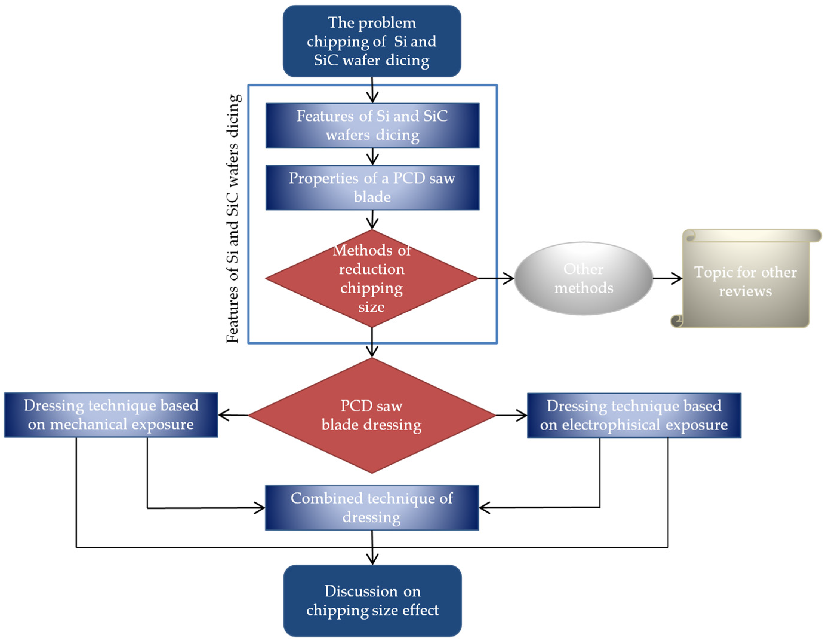
The current review aims to systematize the latest achievements and the most promising methods for polycrystalline diamond saw blade dressing used for dicing Si and SiC wafers, using meta-analysis as the data synthesis method. A meta-analysis is a quantitative combination of study results to identify patterns, discrepancies, or relationships. The schematic of the review structure is provided in Figure 2.

2. Features of Polycrystalline Diamond Saw Blade, Dicing and Dressing

2.1. Features of Dicing as a Step in the Production of Integrated Circuit Packaging

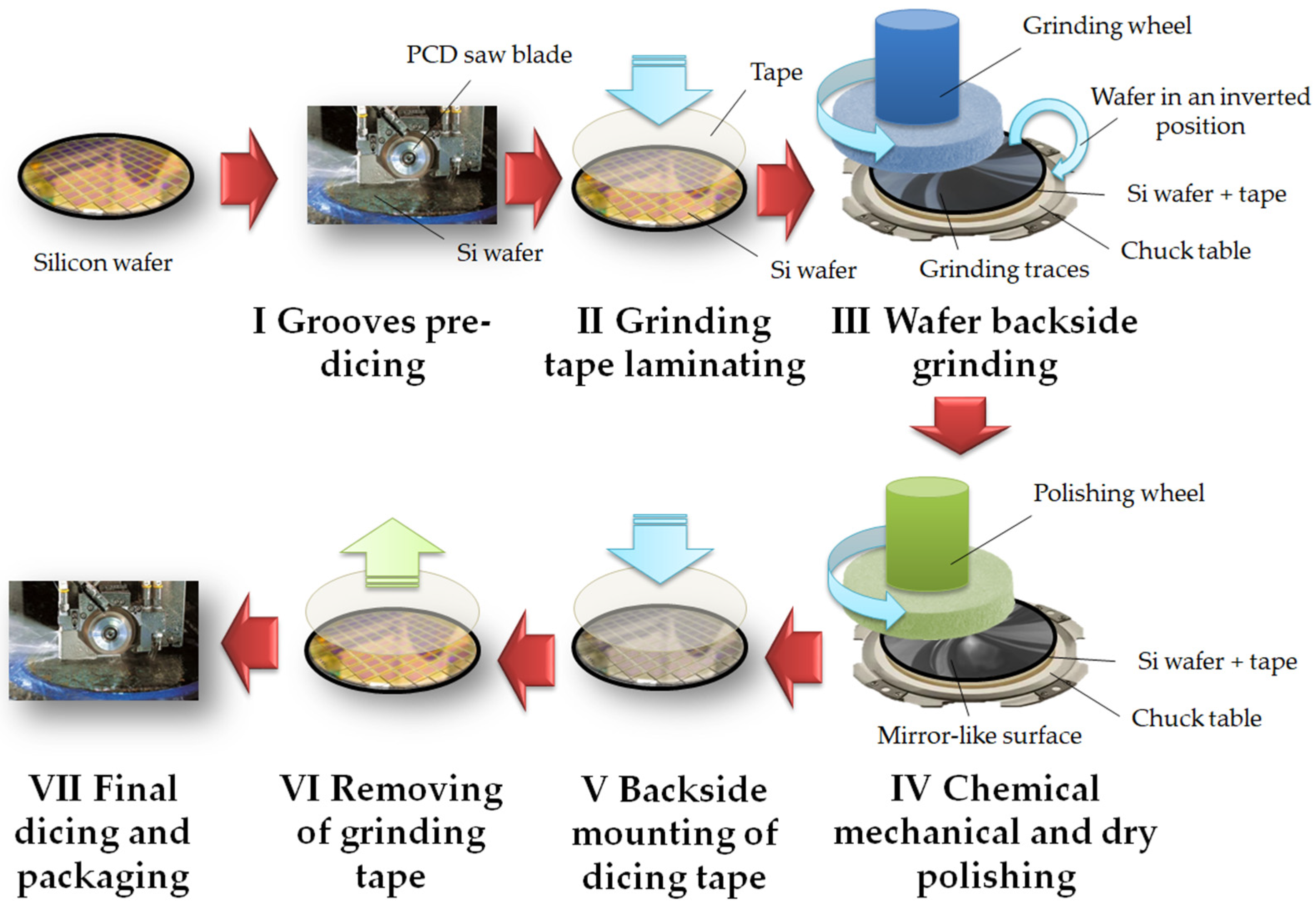
Dicing is a step in the production of integrated circuit packaging in which a wafer (a thin, flat disk of ultra-pure silicon) is cut into thousands of individual pieces, where each piece is called a die; in other words, a small block of semiconductor material on which the functional circuit is produced [15]. Dicing before grinding in silicon semiconductor processing is a popular technique that first involves making a half-cut groove with a PCD saw blade of larger width, followed by simultaneous wafer thinning (grinding and chemical–mechanical and dry polishing to relieve stress), and final die singulation before packaging (Figure 3) [16]. Grinding and chemical-mechanical and dry polishing remove the damaged wafer layer, which is approximately 2 µm thick. Because this approach eliminates the transfer of thinned wafers between technological steps and is mostly implemented on a single piece of equipment using a chuck table to fix a wafer, the risk of wafer damage is significantly reduced [3].
A chuck table for grinding silicon wafers is used in grinding machines for wafer thinning (grinding), where the wafers are clamped on a rotating table with a rotating diamond wheel running through the center. The spindle carrying the wheel moves downward to remove material from the wafer surface, and the wafer is cooled with water to prevent overheating and to remove grinding debris generated during processing. Typically, a rotary chuck table equipped with hydrostatic bearings is used, which ensures high rigidity, that is suitable for grinding large silicon wafers with a diameter of 300–450 mm or a porous ceramic chuck table of round, square, or rectangular shape with a standard size range of 150–540 mm, where the positioning accuracy should not exceed ±1 µm, and the table should not have any visible damage of the subsurface layer that often occurs in dicing. Modern models are also equipped with a tilt adjustment system for the grinding wheel and table spindles [17].

2.2. Properties and Description of a Polycrystalline Diamond Saw Blade

PCD saw blade dressing is a sharpening process for polycrystalline diamond cutting tools that are widely used in cutting non-ferrous metals and alloys (highly abrasive non-ferrous metals, such as silicone aluminum alloys (ADC12, A380), aluminum, copper, brass, and other non-ferrous metals and alloys) [18], composite and plastic materials (processing carbon-fiber reinforced plastic (CFRP), glass-fiber reinforced plastic (GFRP), and glass-fiber reinforced composite materials, which are often challenging due to their abrasive and uneven structure) [19], non-metals (ceramics, quartz, and graphite) [20], abrasive plastics, plastics with mineral fillers [21], and semiconductor materials (silicon, silicon carbide, which are hard to cut by convenient machining) [22]. It should be noted that PCD saw blades are not suitable for cutting ferrous metals, as they often contain carbides that react with the carbide backing, causing increased wear and corrosion.
A PCD saw blade is produced of a composite material made from diamond particles sintered with a metallic (nickel, nickel–cobalt) [12,14,23] or resin binder [24,25,26]. It should be noted that the resin bond of a PCD saw blade is subjected to intensive radial wear and melts under mechanical and thermal loads during dicing, and this type of bond material of a PCD saw blade is not recommended for dicing Si wafers [25]. PCD tools are usually saw blades, milling cutters, and drills, where grit size is from 5 to 30 µm (mainly, ~5–6 µm for high-precision dicing to achieve a chipping width of ~8 µm, and ~8–11 µm for street pre-forming with a chipping width of ~10–14 µm [14]) and a useful diameter of ø55–62 mm [12,14,23,24,25,26]; when the thickness is ~200 µm in dicing SiC substrates [26] and 20–30 µm in dicing Si wafers [12,14,24,25]. Chipping during dicing typically occurs on the back side of the Si wafer (Figure 4). It is important to note that PCD saw blades do not withstand an increased impact of mechanical and thermal loads and break down at temperatures above 700 °C [27]. Dicing Si and SiC wafers typically requires cooling with water at 20 °C and a cooling rate of 1–8 L/min [12,14,23]. Saw blades of PCD exhibit:
  • High hardness and wear resistance, which maintains a sharp cutting edge in machining hard-to-cut materials ((the hardness of the base elements of PCD saw blades is 42–48 HRC, and that is ~405–485 HV when the hardness of polycrystalline diamond grains ranges from 6500 to 7500 HV with a metal (mainly nickel) bond; this value is close to the hardness of pure diamond of 10,000 HV, and that is 30 times harder than the value for hard alloy)) [28]; hardness also depends on the purity, perfection of the crystal structure, and orientation: it is higher in flawless, pure crystals oriented in the direction (along the long diagonal of the cubic diamond lattice) [29];
  • Excellent thermal conductivity, which facilitates rapid heat dissipation and reduces temperature on the contact pad between a tool and workpiece; the thermal conductivity of polycrystalline diamond for saw blades is 700 W/m·K, and that is 1.5–9 times higher than that of cemented carbide and even higher than that of polycrystalline cubic boron nitride and copper [30];
  • Stability under medium operating conditions: at temperatures under 700 °C and pressure.
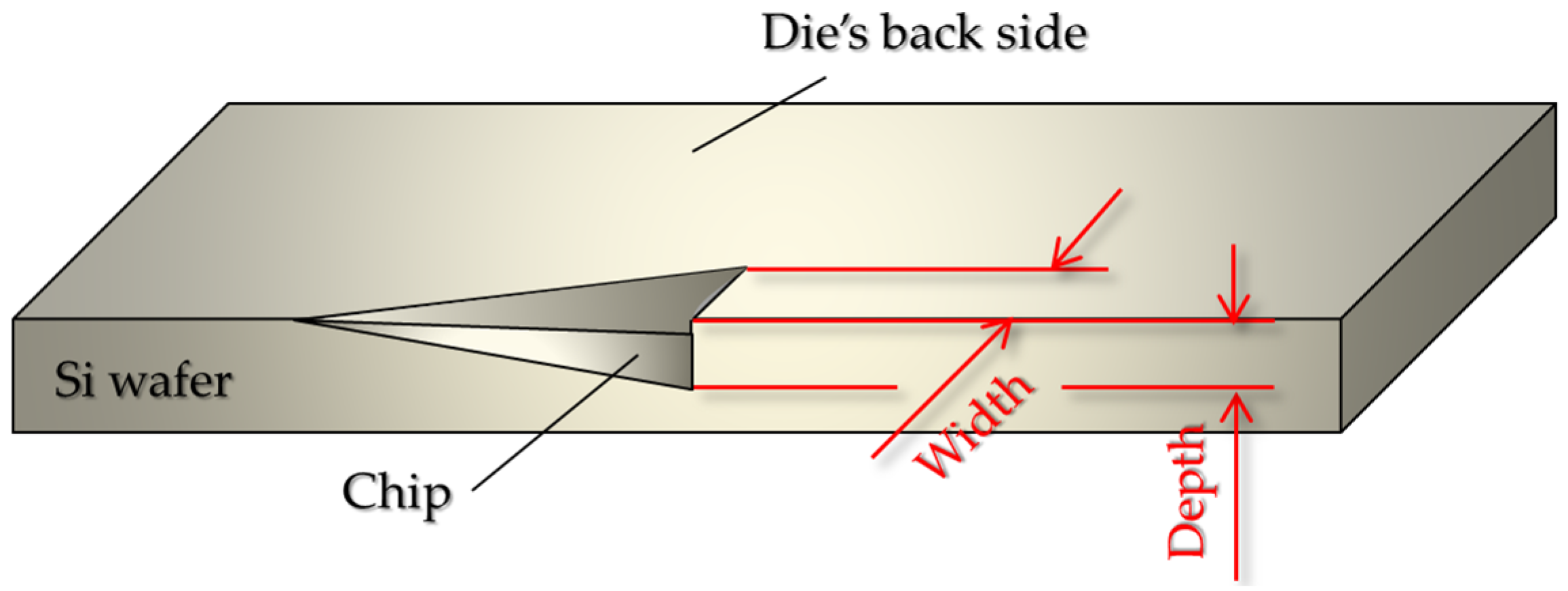
Figure 4. Graphical presentation of a chip formed on a die’s back side during die singulation.
Jmmp 09 00405 g004

2.3. Dressing of a Polycrystalline Diamond Saw Blade

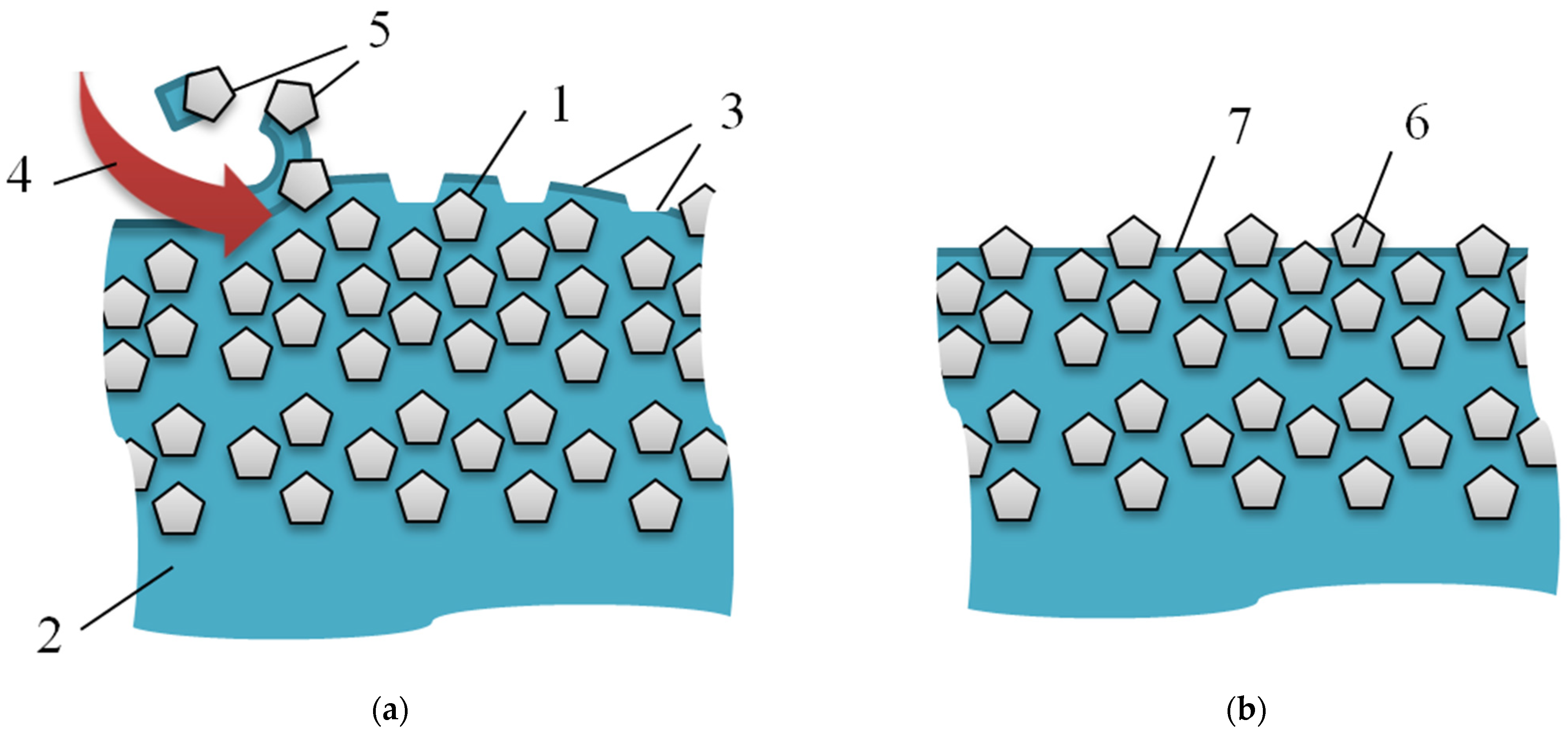
PCD saw blade dressing is vital for removing excess bond material and exposing the diamond particles for machining, as shown in Figure 5. A suitable PCD saw blade profile and geometry are required for the high-precision dicing of Si wafers and SiC substrates and reducing chipping size [31]; the key dressing parameters that control the process are [32,33,34]
  • Medium material used to dress the blade,
  • Dressing modes: feed rate, rotation speed, depth of cut,
  • A number of dressing passes.
During the operation of a PCD saw blade, single diamond grit particles are removed and torn out, leaving empty wells on the surface of the blade tooth’s end face. The formation of the wells is inferred as the diamond falls out from the PCD saw blade surface [35]. They also move along the blade surface due to the binding material’s viscous properties. The side faces of the disk wear out more intensively, and the saw blade profile takes on a specific rounded shape that requires dressing to be more rectangular [36,37].
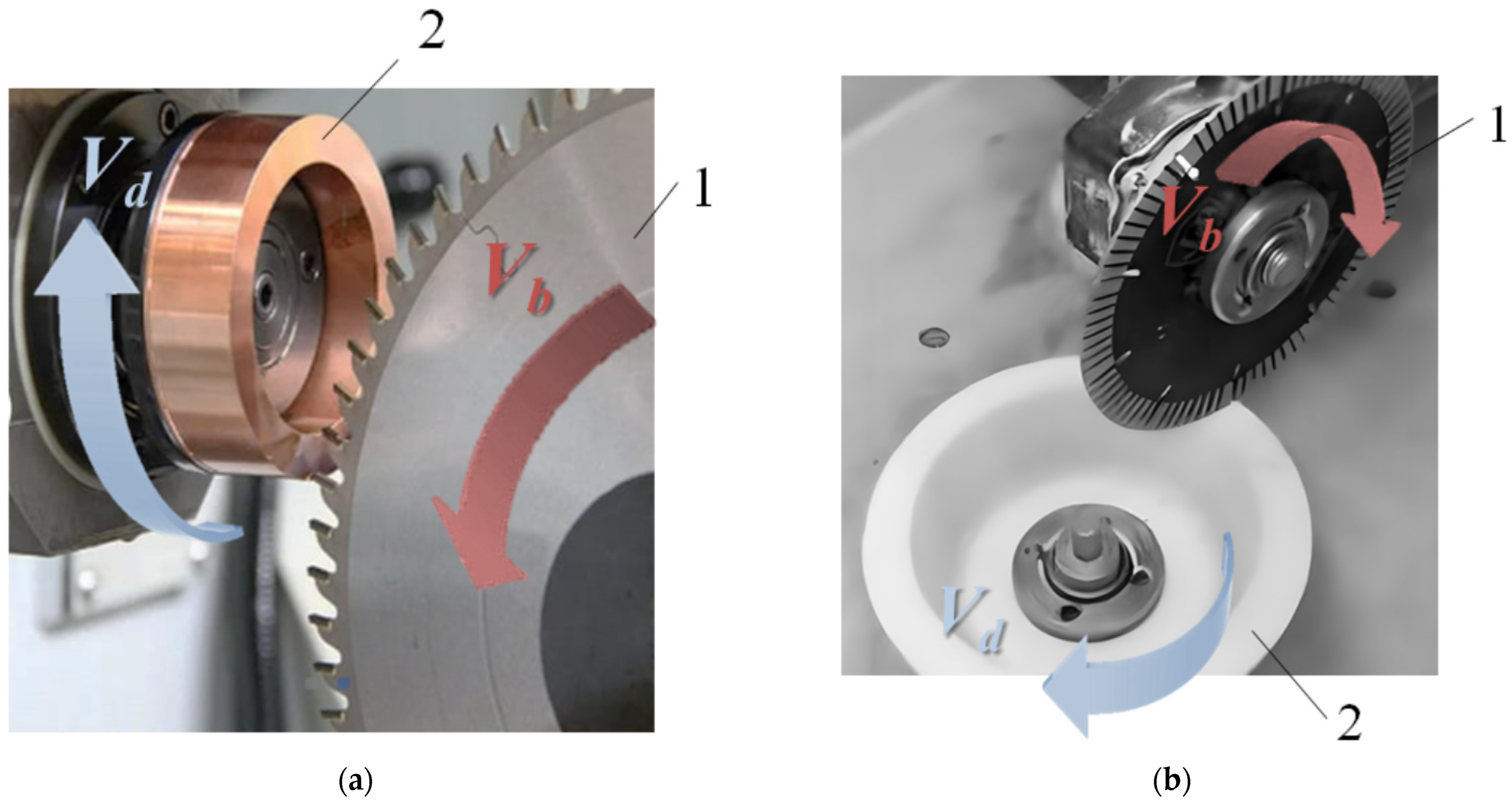
During dressing, the upper layer of the bond and particles is removed mechanically or by electrical erosion, exposing the subsurface layer with diamond particles [14]. The choice of dressing method depends on the condition of a PCD saw blade, including the degree of clogging, the level of grain wear, and the surface curvature (Figure 6). Coolant is highly recommended, since it is used in dicing. Meanwhile, if the dressing has already started, coolant is not recommended because it can easily damage the PCD saw blade due to thermal shock. The dressing of PCD tools is mainly performed by electrical discharge machines or universal sharpening machines, where electrical discharge truing is preferred, as the vibration of the PCD saw blade should be absent or minimized [38]. Inappropriate PCD saw blade dressing technique induces burn marks and other defects in the final IC assembly [35].
Figure 5. A principal scheme of PCD saw blade profile mechanical dressing: (a) in process of dressing, (b) after dressing, where 1 is a single diamond grit particle, 2 is metal bond (nickel), 3 is the profile of the worn PCD blade with wells of removed grit and specific round profile formed during dicing when side material subjects more intensive wear process, 4 is direction of dressing disk rotation, 5 are single diamond particles with adhesive bond material under removing from a PCD saw blade profile, and 6 is a final profile where diamond grit particles are clearly visible on the saw blade surface, 7 is the profile of bond material after dressing, the profile is aligned with the sides and the axis of rotation.
Jmmp 09 00405 g005
Figure 6. Scheme of PCD saw blade dressing: (a) electrical discharge machining (by example of KAMI machine tool, Russia), (b) abrasive dressing (dressing machine tool, Russia), where 1 is a PCD saw blade (diamond wheel), 2 is a dressing tool: a copper electrode tool (a) and an abrasive grinding wheel, flat disk, white electro-corundum (grades: 25–23 A, synthetic corundum with an Al2O3 content of no more than 99%) (b), Vb is rotation direction for a PCD saw blade, and Vd is rotation direction of a dressing tool.
Jmmp 09 00405 g006

3. Methods of Polycrystalline Diamond Saw Blade Dressing

3.1. Mechanical Board Dressing

The mechanical sharpening (dressing) process for PCD saw blades involves several stages [35,39,40]:
  • Rough machining using a coarse-grain diamond grinding wheel;
  • Semi-finishing using a fine-grain grinding wheel;
  • Finishing using a fine-grain grinding wheel.
For high-grain, low-speed grinding wheels, a water-soluble coolant is used to improve grinding efficiency and precision [41,42].
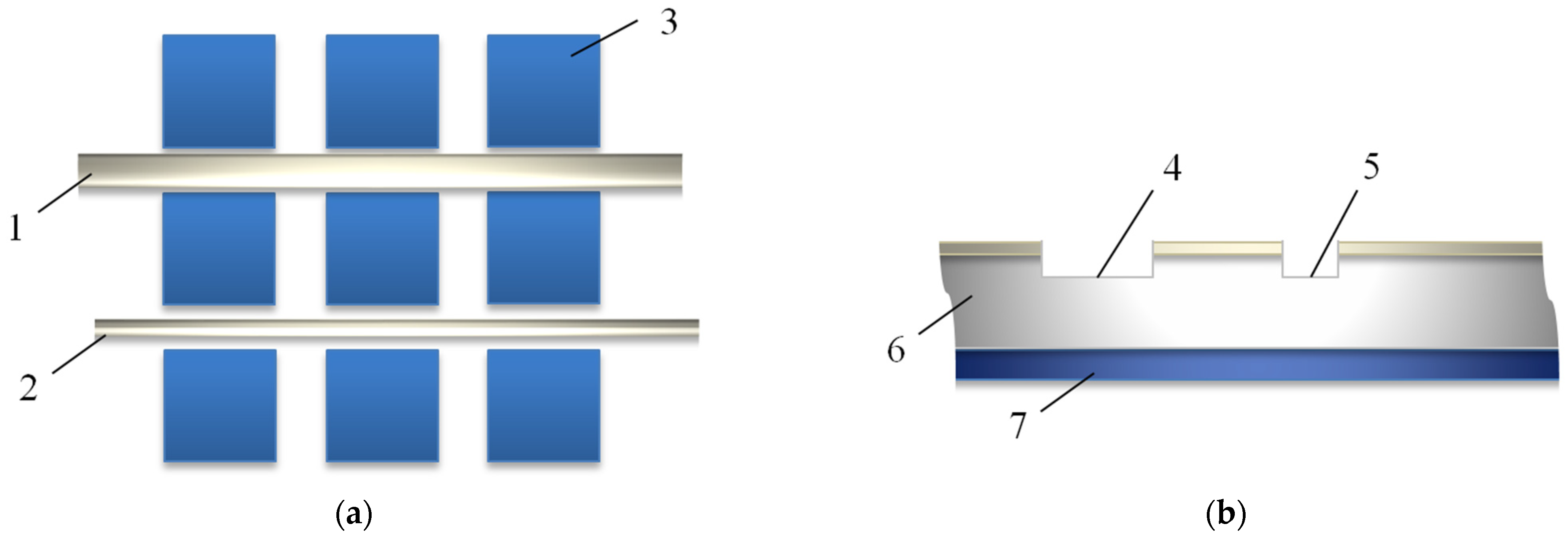
Universal sharpening machines are not suitable, as they do not allow for resharpening the required geometry [43]. In this study, the criterion of efficient dicing (chipping criterion) was chipping of 70 μm (0.070 mm) on the back side of bare die products, and the auto vision reject rate was above 10%. Thus, the authors decide to use the two-wheel dicing technique [3,25,44] to obtain proper visual quality of the wafer back side adhered to the Mylar tape during dicing (Figure 7). The two-wheel technique includes preliminary diing with a larger width (27–32 µm for Z1 and 25–30 µm for Z2 [3]). The wafer back side is important since it is usually seen by the user, and it is used for marking dies. However, it did not bring any significant improvement since many severe lateral and zig-zag (or chevron) back side chippings [12,13,45,46] were observed at each of the dicing steps (preliminary dicing and dicing). Moreover, sidewall chipping propagating from the die back side was detected without any improvement of the dicing street quality. And it destroyed not only the die street edge but also its core (wafer center). The machine used in dicing Si wafers was a DISCO sawing machine (Tokyo, Japan) with automated vision, and that machine has difficulty in detecting the die streets after the first and second dicing. Then, the proposed technique of preliminary dicing and dicing with two PCD saw blades was rejected. Four possible causes of the chipping were mentioned:
  • insufficient cutting power of the second PCD saw blade;
  • improper PCD saw blade dressing (grit exposure);
  • improper pre-cut settings; and
  • low robustness of the technological window.
After taking the measures to regulate each of those issues, the back side chipping size was significantly reduced and did not exceed 15 µm. Then, the authors reduced the feed rate of dressing as a general recommendation. However, it did not provide any positive effect and caused even more intensive chipping.
Figure 7. Scheme of two-wheel dicing technique at a DISCO sawing machine: (a) a scheme of automated dicing in plan, (b) a left view of dicing, where 1 is a PCD saw blade (diamond wheel) of a larger width, 2 is a PCD saw blade (diamond wheel) of a smaller width, 3 is a single die, 4 is a path (die street) after a thicker PCD saw blade, 5 is a path after a thinner PCD saw blade, 6 is a Si wafer, and 7 is thermo-resistant Mylar tape.
Jmmp 09 00405 g007
The authors of [47] proposed that a machine with a reciprocating feed is a more effective way of truing and dressing sintered diamond saw blades compared to a direct feed.
The dressing of metal-bonded diamond saw blades using four methods was considered in [48]: stirring in rock slurries, grinding with Al2O3 wheels, dressing with SiC wheels, and dressing through sawing refractory materials. The protrusions generated by the surface grinding with alumina wheels were the smallest. The height of grit protrusion for either SiC dressing or refractory sawing was about 20% of the average diamond size, which is optimal for segment sawing performance. Changes in spindle power during the sawing of refractory materials can be used to in situ monitor dressing.
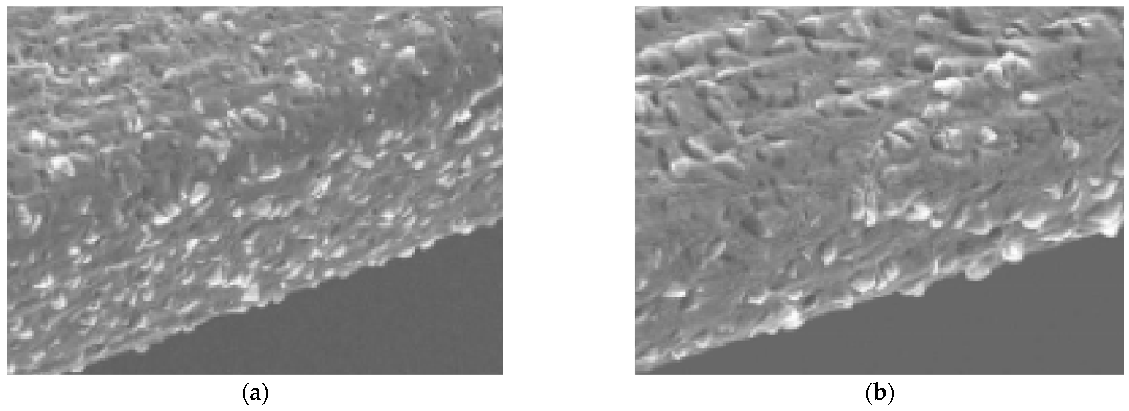
The new board-dressing method, which takes less than an hour to complete the saw-blade dressing for wafer dicing, was proposed by K.W. Shi et al. [49]. The fine diamond grits of the saw blade are dressed on a 75 × 75 mm SiC dresser board with a thickness of 1 mm, mounted on a ~0.090 mm tape containing equivalent or finer SiC grits, while the coarse diamond grits require a rougher SiC grit. Two saw blades (Z1 and Z2, two-wheel dicing technique) with a diamond grit size of 3500 and standard and soft bonds were used for dicing a CMOS 90 nm low-k wafer: die sizes of 4 × 4 mm and 7 × 7 mm, wafer diameter of 300 mm, wafer thickness of 280 µm, and saw street width of 80 µm. The saw process parameters for dicing C90 low-k in assembly were 45,000–55,000 rpm and 25,000–35,000 rpm for two types of blades (Z1 and Z2), cut depth into Si wafer of 60–160 µm (Z1) and into dicing tape of 25–50 µm (Z2), and table speed of 20–40 mm/s. The dressing was performed with SiC dresser boards of grit sizes less than 3500 and greater than 3500, and the results were compared with those obtained with a 300 mm Si wafer. The key dressing parameters were the number of dressing passes, table speed, and dressing cut depth. The SiC dresser board’s efficiency criterion was die top side chipping (%). Table speed, depth of cut, and the dressing tool are key factors for top side chipping. Faster table speed and a larger dressing cut depth are preferred to improve the top side chipping performance for the dresser board with a grit size of 3500 or higher (0.77% at 31 dressing passes, compared to 1.73% for the control Si wafer at 2500 dressing passes). The SiC dresser board with a grit size less than 3500 has shown better results at a lower table speed and a higher dressing cut depth, with 21 passes and top side chipping of 0.91%. The experiments have shown that dressing with a Si wafer takes a few hours, while dressing with a SiC dresser board with more than 3500 grit size takes less than an hour and significantly improves blade dressing performance. The kerf profile after sawing with a dressed blade on a Si wafer is sharp (Figure 8), which negatively affects the final quality of C90 low-k assembly. The kerf profile after sawing with a dressed blade by a SiC dresser board is more rounded and still not rectangular, but it is more suitable for dicing than a sharp one. The images of the optical microscope (Figure 9) demonstrate the character of Si wafer chipping in dicing by a PCD saw blade after dressing by Si wafer, SiC board with lower grit size (<3500), and SiC board dresser with greater grit size (>3500). As it is seen, the chipping size is larger than a die street of 80 µm for a PCD tool dressed by a Si wafer (frequency of chipping is one chipping per 10 cut lines) (Figure 9a). Dressing with a SiC board dresser with a lower grit size (<3500) caused even more frequent chipping (10 chippings per 10 cut lines) (Figure 9b). Dressing with a SiC board dresser provided the better result: chipping is less than the width of a die street, 80 µm, and the frequency of chipping is one chipping per 10 cut lines (Figure 9c). The main techniques in PCD saw blade mechanical sharpening are compared and provided in Table 1.

3.2. Electrical Discharge Truing/Grinding

Electrical discharge machining (EDM) is used to machine complex shapes of hard-to-machine materials that are difficult to machine with conventional processes. The material of the workpiece is removed by the thermal energy of the electrical pulses between the workpiece and the tool, which are both electrodes. Material is removed due to sublimation at the plasma’s temperature, generated by the discharge channel (of 10.000 K) [50]. When the electrical pulse is interrupted, the particles of the sublimated material are solidified in the working fluid (water or hydrocarbons) and washed out of the interelectrode gap, which is 0.050–0.075 mm wide, depending on the electrical conductivity of the material to be processed (as the more electrically conductive the material is, the wider the interelectrode gap) [51,52]. The technology can be applied to electrically conductive materials regardless of their hardness, including oxide ceramics when carbide powder is added [53,54,55]. Moreover, there are many techniques for subjecting insulating materials to electrical discharge [56].
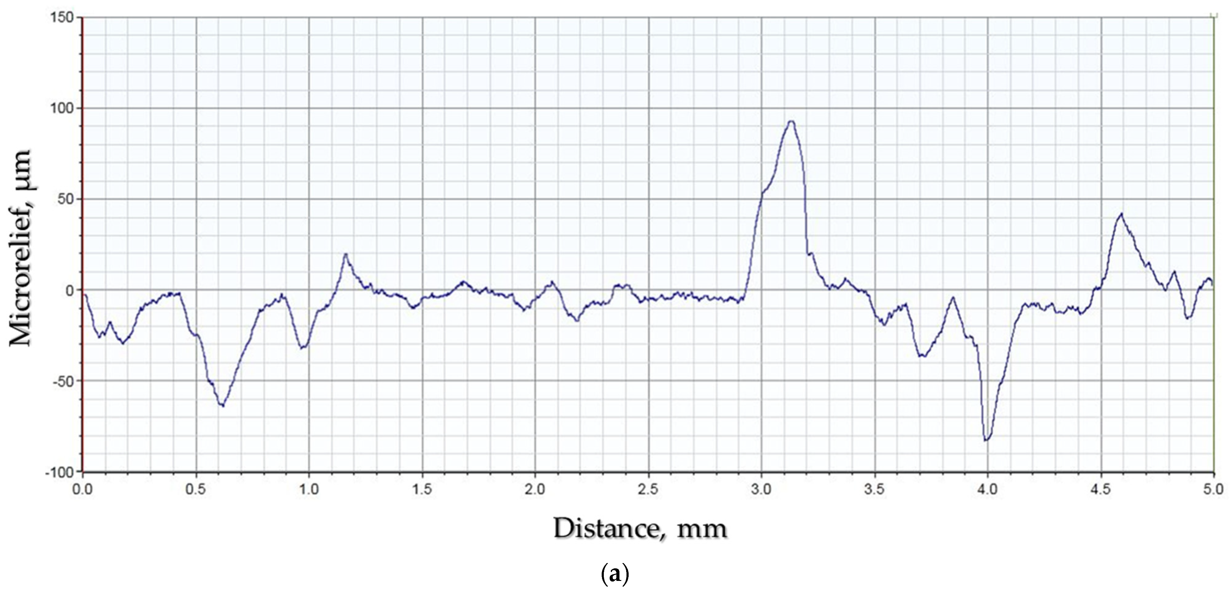
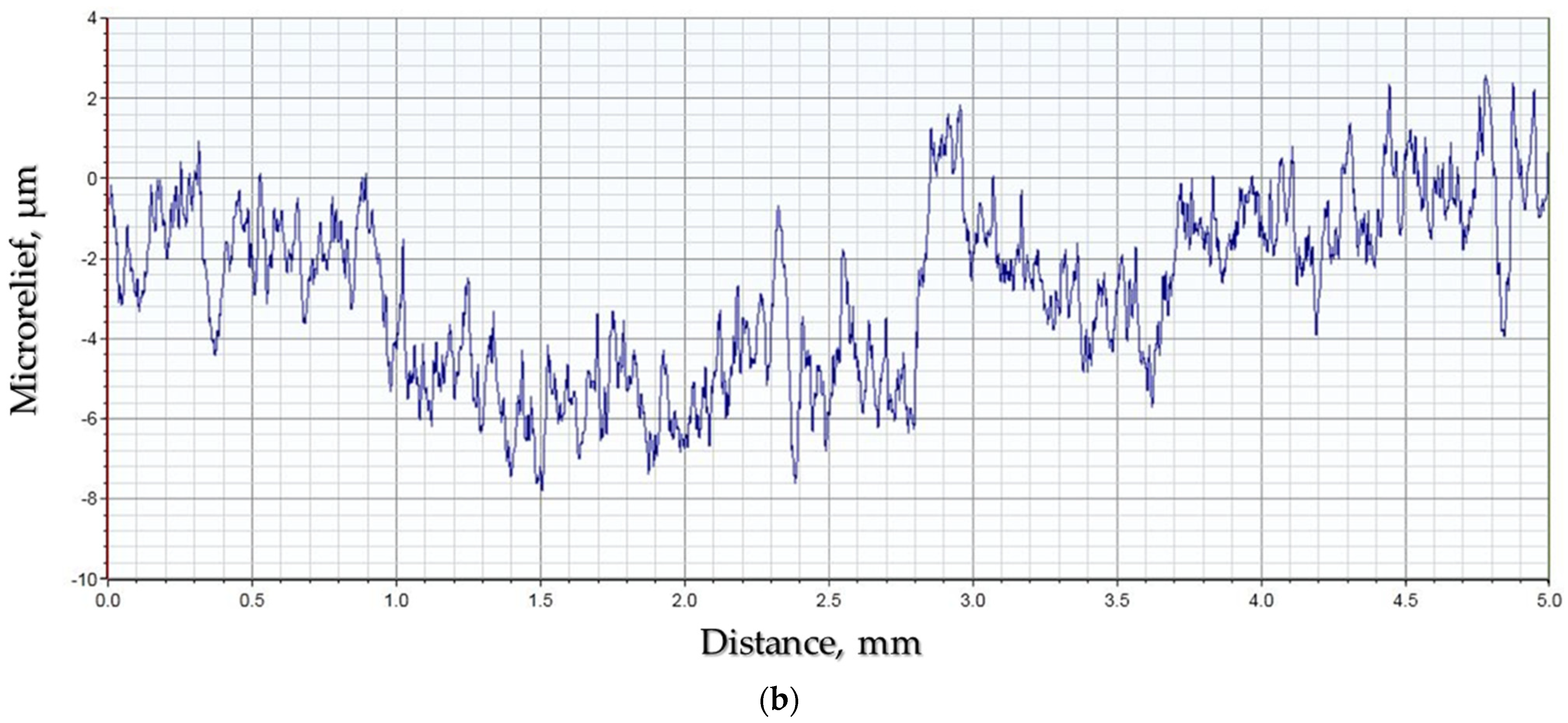
Specialized electrical discharge machines are used to sharpen PCD saw blades: an electrical discharge grinding method with a disk electrode was proposed in [57]. Two types of electrode disks were used in electrical discharge grinding: graphite and copper. The influence of processing factors—gap voltage, electrode-wheel rotation speed, and pulse duration—on the performance and surface quality of the PCD saw blade was investigated (Figure 10). It was shown that pulse duration exhibits the most impact on the machining rate. A copper electrode can produce a smoother surface than a graphite one in electrical discharge grinding (Figure 11). Edge sharpening of a PCD tool with a diameter of ø125 mm was performed with circular run-out errors < 0.050 mm.
It should be noted that the rotational speed of the electrode wheel (tool electrode) during electrical discharge dressing (truing) affects the material removal rate. It is because the rotational motion of the wheel-electrode ensures a continuous and uniform flow of dielectric fluid (deionized water or mineral-oil-based dielectric fluid) through the interelectrode gap between the wheel-electrode and PCD saw blade under dressing/truing. In this context, electrical discharge machining removes material from the conductive workpiece (PCD saw blade) by exposing electrical discharges, and the rotational motion of the wheel-electrode helps ensure a uniform discharge distribution [58,59]. For example, the optimal processing speed of the electrode wheel is 3.3–5.0 mm/s, then the rotation speed is about 1000–6000 rpm.
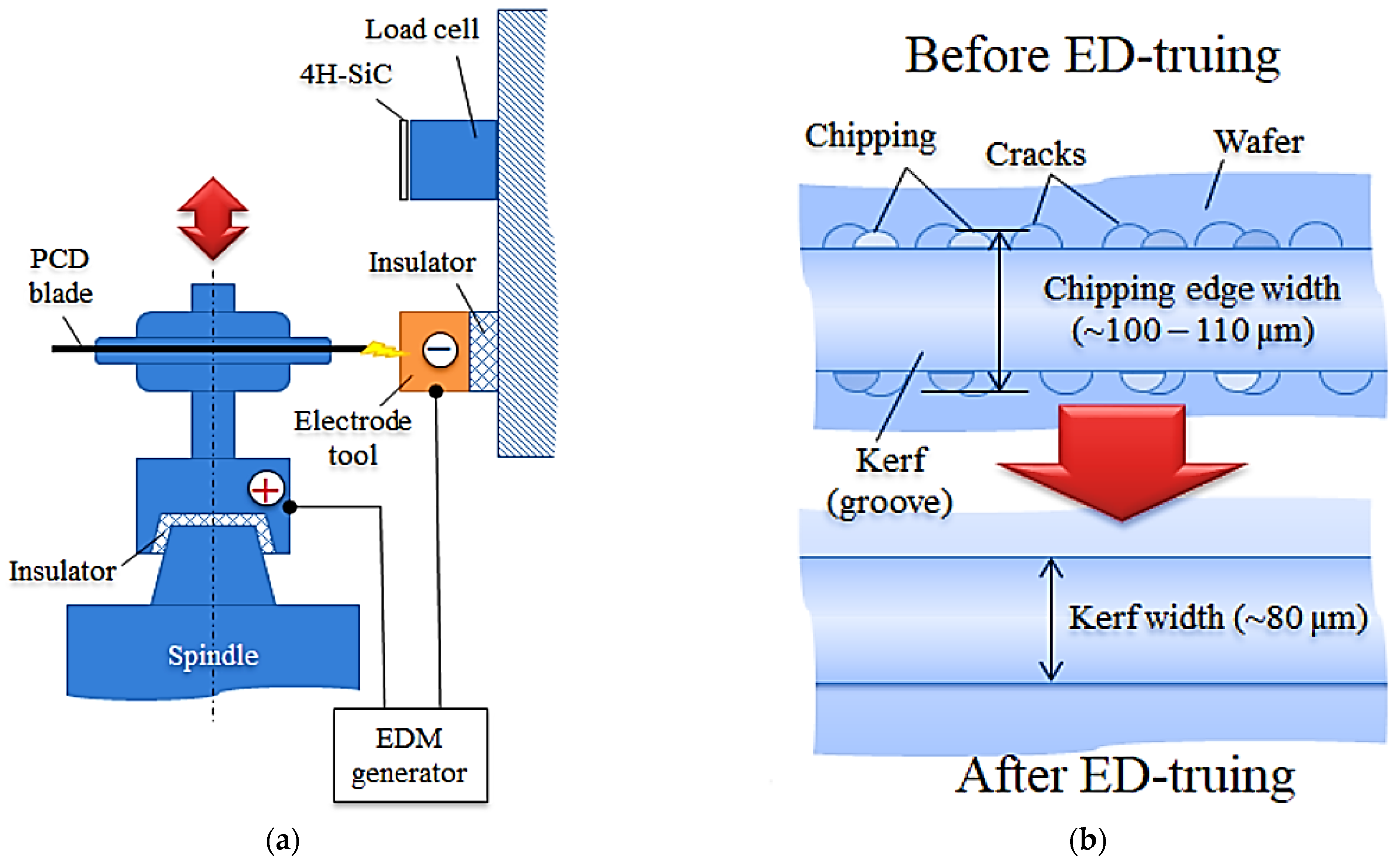
The effect of electrical discharge truing with two dielectric types was researched by K. Watanabe et al. in [60]. The PCD saw blade with cobalt (Co) bond material was exposed to electrical erosion under the following conditions: discharge current of 1 A, open-circuit voltage of 100 V, and discharge duration of 0.4 μs; the working fluid was pure water with a specific electrical resistance of 1.0 × 10⁷ Ω·cm and an oil-based dielectric. The PCD blade thickness was 50 μm, the diameter was 50 mm, the diamond grain size was 0.5 μm, the polarity of the blade was positive (+), and the polarity of the tool electrode was negative (−). The cathode was made of a tungsten–copper alloy (usually copper of 10–50% [61,62]) and was fixed when the PCD blade rotated. The PCD saw blade was controlled at 1 µm increments during dressing (Figure 12a). Further, the dressed PCD saw blade was tested on a polymorph of silicon carbide (4H-SiC) workpiece with a thickness of 0.34 mm, at a rotation speed of 8000 min–1, a feed rate of 15 mm/min, and a cutting depth of 50 μm (Figure 12b). The problem was the influence of electrical discharge truing as a dressing operation on the blade’s operational ability. Since electrical erosion negatively influences the surface under exposure [63,64], the surface and subsurface layer lose chemical elements and become more brittle due to deposition of the secondary structures of the second order (oxide films in the case of electrical discharge machining in water) and the specific crater-like surface of material droplets and cracks [65]. The research should show that the PCD saw blade surface is subjected to electrical erosion up to 20 µm (as the so-called “white layer” of deposited oxides of the metals, metalloids and/or non-metals, poor of bond material, cobalt in this context [66,67]). During electrical discharge truing in water, the smallest surface roughness parameter Rz was 3 µm, whereas in oil-based working fluid it was 1 µm. The flexural strength was 2.2 GPa for the polished blade, 2.0 GPa for the machined blade in water with a roughness Rz of 3 µm, and 2.4 GPa for the machined blade in oil (as lower roughness, as higher flexural strength). The testing with the non-trued PCD saw blade and the PCD saw blade after electrical discharge truing has shown that there was no visible chipping in 20 m of dicing for the blade after electrical discharge machining at a kerf (groove) width of 80 µm when the chipping size was 20–30 µm at each side of the kerf for non-trued PCD blade, then the chipped kerf width was of 100–110 µm (Figure 13).

3.3. Mechanical Dressing, Coating, and Redressing Technique

J.P. Chu et al. [68] proposed a method of coating diamond dicing blades with metallic glass (amorphous alloy with metallic conductivity, the specific electrical resistance of which is about 100-300 μOhm cm, which is significantly higher than the resistance of crystalline metals) to reduce chipping in sawing Si, SiC, sapphire, and patterned sapphire substrates (PSS). It should be noted that vacuum plasma thin coatings play a significant role in modern industry, prolonging the service life of tools [69]. However, they require specific equipment and stages of preprocessing, such as cleaning functional surfaces with neutral atoms [70,71,72]. The method includes dressing, coating the PCD blade with metallic glass, and redressing to bare PCD grit particles (Figure 14). The workpieces were
  • Silicon wafer (in electronics for the production of integrated circuits and in photovoltaics for traditional solar cells) of 525 µm thick (with a tolerance of ±1%), ~10.16 cm (4 in.) in diameter (with a tolerance of ±1%), surface orientation of <100> (with a tolerance of ±0.5°), p-type (contains boron as a dopant) (for Si wafer S 6075, Otto Chemie Pvt Ltd., Mumbai, India, the specific electrical resistance of more than 200 Ω·cm, roughness parameter Ra of less than 0.8 nm);
  • SiC 4H-N wafer (in optoelectronics) of 350 µm thick (with a tolerance of ±25 µm), ~10.16 cm (4 in.) in diameter (with a tolerance of 0.5 mm), surface orientation of <0001> (with a tolerance of ±0.5°), 4H-polytype, n-type (for 4H SiC epitaxial wafers with a single crystal film/epitaxial layer on the SiC substrate for MOS fabrication, where wide-band semiconductor devices are made on this film and SiC is the substrate, in other words, forming heteroepitaxial structures, structures in which the growing layer differs in chemical composition from the substrate material, possible only for chemically non-interacting substances, with films of other wide-bandgap semiconductors (GaN, AlN, ZnO) on a SiC substrate, in the described case, gallium nitride (GaN) is the epitaxial layer, Xiamen Powerway Advanced Material Co., Ltd., Xiamen, China, growth method: CVD [73,74], the specific electrical resistance of 0.015–0.028 Ω·cm, roughness parameter Ra < 1 nm on the C face);
  • Sapphire/PSS (in LED manufacturing, sapphire allows for the growth of GaN crystals, which emit light when an electric current is applied, and in optics, due to the high transparency and hardness, sapphire wafers serve as windows and lenses in high-pressure and high-temperature environments, as well as in infrared imaging systems) of 430 µm thick (with a tolerance of ±25 μm), ~50.8 cm (2 in.) in diameter (with a tolerance of ±0.1 mm), surface orientation of <0001> (C-plane, with a tolerance of ±0.2°), (monocrystalline Al2O3, high purity (99.999%), roughness parameter Ra 0.8–1.2 µm); the PSS pattern is 2.6 µm in height and in 2.35 µm in diameter.
Figure 14. PCD tool profile of dressing–coating–redressing technique: (a) after metallic glass coating, (b) after redressing, where 1 is a single diamond grit particle, 2 is metal bond (Fe-Co-Sn), 3 is the profile of the PCD saw blade after dressing, 4 is the profile of metallic glass (Zr-Cu-Al-Ni amorphous alloy) coating of 200 nm after the deposition on the pre-dressed PCD blade (the coating is marked red), 5 is the profile of metallic glass coating after additional (second) dressing, and 6 is a final profile where diamond grit particles are clearly visible on the saw blade surface and the profile is aligned with the sides and the axis of rotation.
Jmmp 09 00405 g014
Dicing factors were as follows:
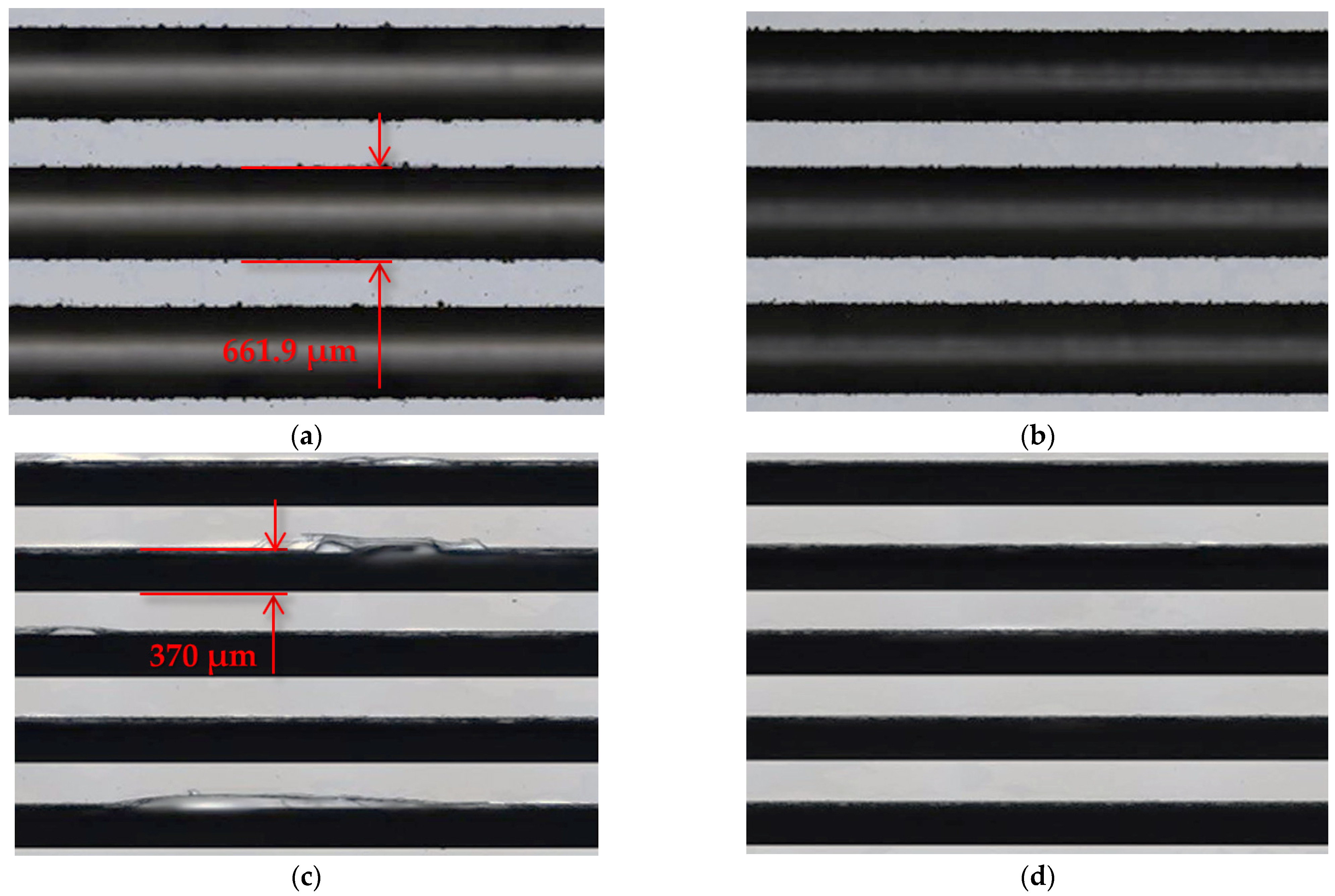
  • Direction of <110> with a depth of 400 µm (2 passes of 200 µm of dicing), width of 661.9 µm, 20 kerfs for Si wafer;
  • Direction of < 11 2 ¯ 0 > with a depth of 200 µm (2 passes of 100 µm of dicing), width of 370 µm, 20 kerfs for SiC wafer;
  • Direction of < 11 2 ¯ 0 > with a depth of 100 µm (2 passes of 100 µm of dicing), width of 315 µm, 20 kerfs for sapphire/PSS.
The dicing tool was a diamond blade MBT-5885 SD800N50M51 (Disco, Tokyo, Japan) and a Fe-Co-Sn sintered diamond dicing blade (Asahi, Taoyuan, Taiwan) with a diamond grit size of 22/36 μm, outer diameter of ø58 mm, thickness of 0.89 mm, and a chamfer of 60°. The coating deposition, of the following composition, 61.7 at.% of Zr, 24.6 at.% of Cu, 7.7 at.% of Al, and 6.0 at.% of Ni, was performed at a base pressure of <9.3 × 10⁻⁴ Pa and working pressure of 5.0 × 10⁻⁴ Pa and power of 2.5 kW on a high-power impulse magnetron sputtering system (Highpulse Bipolar 4002 G2, Freiburg im Breisgau, Germany). The target was ~15.24 cm (6 in.). For the deposition of 200 nm of coating, the samples were placed at a distance of 8.68 cm; the deposition rate was 6.07 nm/min. Before coating, the blade was subjected to dressing with a WA600L whetstone (Asahi, Mona Vale, Australia). During the initial dressing (the first stage, preliminary dressing), 10 kerfs were produced at a depth of 400 μm, with a spindle speed of 35,000 rpm, a feed rate of 5 mm/s, and cooling with deionized water. An additional dressing after coating deposition allowed the removal of the metallic glass coating from the diamond grit surface. After the second dressing, the mentioned samples were diced at 25,000 rpm, and other conditions were similar to those during dressing.
The method allowed reducing the coefficient of friction and the chipping area fraction. The chipping area fractions were reduced by 23% for the Si wafer, 36% for the SiC wafer, 45% for the sapphire substrate, and 33% for the PSS substrate (Figure 15). When dicing silicon wafer and sapphire substrate, the most significant effect from using the metallic glass coating was achieved at the first kerfs (about 84% for Si and 96% for Al2O3); on the 20th kerf, the effect was less (18% for Si and 80% for Al2O3). When dicing silicon carbide wafers and PSS, the opposite trend was observed: at the first kerfs, the effect was insignificant (64% for SiC and 92% for PSS); by the 20th kerf, the effect became more obvious (94% for SiC and 98% for PSS). In dicing sapphire and PSS, the effect was higher and changed insignificantly.

4. Discussion

The collected data on the influence of the PCD saw blade dressing methods based on the three types of exposure (mechanical, electrical discharge, combined technique) on chipping size are summarized in Table 2. The criteria for Si and SiC wafer dicing efficiency were chosen as chipping parameters (size, width, area), or, where such data were not clearly presented or corresponding experiments with Si and SiC wafers were not conducted, any other effects on the street edge or surface quality.
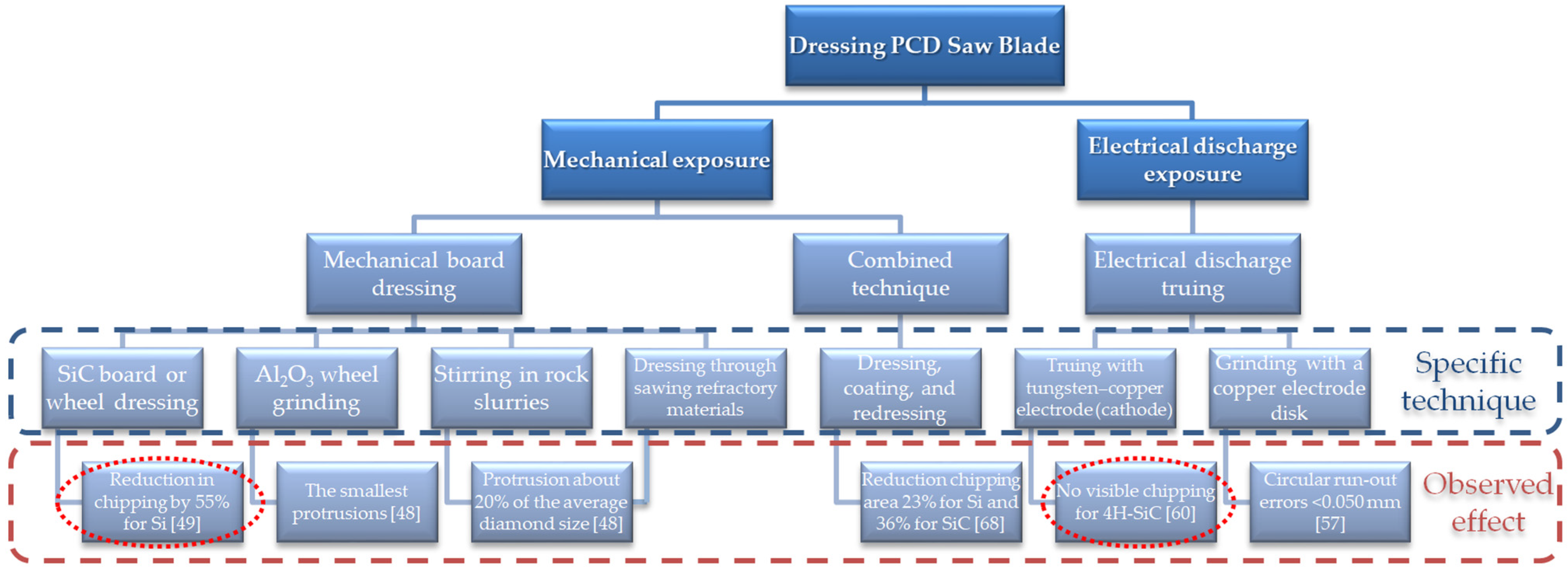
The considered methods, techniques, and approaches for reducing chipping size and width during dicing of Si wafers and SiC substrates by dressing a PCD saw blade are presented in Figure 16. It was observed that the minimum chipping size in dicing 4H-SiC was achieved with no visible chips at a first distance of 20 m, using the PCD saw blade electrical discharge truing (dressing) method with a tungsten–copper electrode wheel [60]. SiC board dressers have also shown significant reductions in chipping during the dicing of Si wafers (55%) [49]. Both techniques require specialized equipment; however, they can be implemented in a single step by clamping the wafer to a chuck table. The comparison of chipping sizes on the back side of Si and SiC wafers for each dressing method is provided in Table 3.
Thus, it is recommended to follow proper technique, use specialized machines and recommended tools, and observe safety precautions to sharpen PCD saw blades with the purpose of reducing chipping size in dicing Si and SiC wafers. The goal of sharpening is to restore the cutting edge’s sharpness: to reduce the circular waviness, to remove the rounded profile, making the profile of the PCD saw blade profile more rectangular, and to remove the bond material to expose under-layered PCD grains so that the dicing exhibits the minimum possible chipping of the die streets.
Among the considered dressing techniques based on the various natures of the physical exposure, the most remarkable results were demonstrated for electrical discharge truing with a tungsten–copper electrode. No chipping was observed after 20 m of dicing distance for a 4H-SiC wafer [60]. Electrical discharge grinding with a copper electrode disk has also shown a reduction in circular run-out error, but the reduction in chipping size was not reported [57]. At the same time, SiC board wheel dressing has shown a reduction in chipping by 55% in dicing Si wafers [49]. The most minor protrusions were demonstrated in grinding with an Al2O3 wheel [48], when stirring in rock slurries and dressing through refractory materials, which showed a reduction of 20% in average diamond size. It should be noted that, due to the relatively similar physical and electrical properties of Si and SiC, the dressing methods and techniques used in sharpening PCD saw blades for dicing one of those materials can be extended to the other one. The general recommendations are as follows (Table 4):
  • In mechanical dressing, the grit size of the dressing wheel should be higher than that of the PCD saw blades (a SiC board is recommended compared to a Si wafer as a dresser [49]); the grit size of the PCD saw blade is better above >3500;
  • In electrical discharge truing/grinding, the specific electrical conductivity of the electrode (cathode) should be higher than those for the bond material of the PCD saw blade (preferably a copper electrode, if possible, due to the properties: copper has high electrical and thermal conductivity, while tungsten has high brittleness, low ductility, and high abrasiveness; the electrical conductivity of tungsten is almost three times lower than that of copper [74]); the recommended factors are the discharge current of 1 A, the circuit voltage of 100 V, and the discharge duration of 0.4 μs;
  • During dressing/truing the profile of the PCD saw blade on both the rake and flank faces, approximately 0.05–0.15 mm of bond material should be removed;
  • Equal forces of mechanical or electrical exposure should be applied to each cutting face, receiving the same number of passes to sharpen the entire PCD saw blade evenly;
  • The profile of the PCD saw blade should remain perpendicular to the dressing/truing surface to ensure proper processing;
  • The cutting edge radius should not exceed 0.1–0.2 mm; thus, the dressing/truing should be monitored;
  • A coolant during mechanical dressing is a water-based coolant, as PCD is a hard material with insufficient heat resistance [75]; for electrical discharge truing, an oil-based working fluid is recommended to provide better roughness parameter Rz (1 µm) [60];
  • When sharpening with coolant, the coolant flow should be over the entire grinding wheel surface to avoid thermal shock and damage to the PCD saw blade; the same applies for the electrical discharge truing; it is better when the entire PCD wheel is in dielectric fluid to avoid deviation of the shape and sizes;
  • The optimal coolant flow prevents excessive wear of a dresser and damage to the cutting edge due to insufficient fluid or intermittent flow; the optimal flow in electrical discharge machining is necessary to remove debris from the interelectrode gap, avoiding short circuits.
The important issues are to perform manipulations with the PCD saw blade when the sharpening/truing machine is off and to be at a safe distance from the sharpening or grinding process to eliminate the possibility of injury from ejecting particles and debris from the saw blade.
Table 4. The recommendations for dressing the PCD saw blade by techniques based on mechanical and electrophysical exposures.
Dressing ParametersPCD Saw Blade Dressing Technique
Mechanical DressingElectrical Discharge Truing/Grinding
Dressing tool requirementsHigher grit size (>3500), preferably SiC dresserMore electrically conductive than bond material (preferably copper; if increased rigidity is required, tungsten–copper; polarity is negative)
Dressing factorsFeed rate of 10–50 mm/s, rotation speed of 15–50 min−1, dress passes of 20–70 linesDischarge current of 1 A, circuit voltage of 100 V, discharge duration of 0.4 μs, interelectrode gap of 0.050–0.075 mm
Coolant/working fluidWater-based, optimal flow on the contact pad and over the entire bladeOil-based (hydrocarbons), optimal flow in the interelectrode gap and over the entire blade
General safety requirements
  • Manipulations with the PCD saw blade when the machine is off;
  • Provide a safe distance from the dressing to eliminate the possibility of injury.

5. Conclusions

In the review, several techniques for PCD saw blade dressing were considered to minimize chipping size (width and area), which is a problem in manufacturing integrated circuits. The observed techniques were separated into two groups based on the nature of the exposure during dressing: mechanical and electrical discharge. Both techniques have shown significant results in reducing chipping at the street edge. During electrical discharge truing over 20 m of dicing, cracks and defects at the chipping edge were not observed, whereas without the dressing technique, the chipping size is about 20–30 µm, which can have a significant impact on dicing die streets of 60–80 µm width. Using the SiC board dresser technique, the maximum reduction in chipping was 55% during dicing a Si wafer. The use of the combined technique “dressing–coating–redressing” has shown a less pronounced effect of 23–36%. The summarized data are intended for further research to identify prospective future directions for minimizing chipping size, determine the most promising and advanced approaches, and identify those that have the most significant effect in modern industry, promoting the switch to the sixth technological paradigm.

Author Contributions

Conceptualization, S.N.G. and M.A.V.; methodology, S.N.G. and A.S.M.; software, K.H. and A.A.O.; validation, K.H. and A.A.O.; formal analysis, A.S.M.; investigation, A.A.O.; resources, A.S.M.; data curation, A.S.M.; writing—original draft preparation, K.H. and A.A.O.; writing—review and editing, A.A.O. and M.A.V.; visualization, K.H. and A.A.O.; supervision, S.N.G.; project administration, M.A.V.; funding acquisition, M.A.V. All authors have read and agreed to the published version of the manuscript.

Funding

The research was financially supported by the Ministry of Science and Higher Education of the Russian Federation (project No. FSFS-2023-0003).

Data Availability Statement

The original contributions presented in the study are included in the article, further inquiries can be directed to the corresponding author/s.

Conflicts of Interest

The authors declare no conflicts of interest.

References

  1. Qin, H.; Mo, Y.; Xun, Q.; Zhang, Y.; Dong, Y. A Digital-Controlled SiC-Based Solid State Circuit Breaker with Soft Switch-Off Method for DC Power System. Electronics 2019, 8, 837. [Google Scholar] [CrossRef]
  2. Hwang, S.; Won, J.; Lee, J.; Lee, E. A Study on Statistical Analysis of Si-Wafer Polishing Process for the Optimum Polishing Condition. Key Eng. Mater. 2008, 389–390, 493. [Google Scholar] [CrossRef]
  3. Su, T.-J.; Chen, Y.-F.; Cheng, J.-C.; Chiu, C.-L. Optimizing the dicing saw parameters of 60 μm wafer dicing street. Microsyst. Technol. 2018, 24, 3965–3971. [Google Scholar] [CrossRef]
  4. Efrat, U. Optimizing the wafer dicing process. In Proceedings of the 15th IEEE/CHMT International Electronic Manufacturing Technology Symposium, Santa Clara, CA, USA, 4–6 October 1993; pp. 245–253. [Google Scholar] [CrossRef]
  5. Debao, Y.; Fei, Q.; Jinglong, S.; Zhongkang, W.; Liang, T. Subsurface damage distribution of ground silicon wafers. In Proceedings of the 15th International Conference on Electronic Packaging Technology, Chengdu, China, 12–15 August 2014; pp. 871–873. [Google Scholar] [CrossRef]
  6. Zhang, C.; Liang, X.; Cheung, C.F.; Wang, C.; Bulla, B. Theoretical and experimental investigation of ultrasonic cutting kinematics and its effect on chip formation and surface generation in high-frequency ultrasonic vibration-assisted diamond cutting. J. Mater. Res. Technol. 2024, 30, 5662–5676. [Google Scholar] [CrossRef]
  7. Shen, J.; Zhu, X.; Chen, J.; Tao, P.; Wu, X. Investigation on the Edge Chipping in Ultrasonic Assisted Sawing of Monocrystalline Silicon. Micromachines 2019, 10, 616. [Google Scholar] [CrossRef]
  8. Fuegl, M.; Mackh, G.; Meissner, E.; Frey, L. Assessment of dicing induced damage and residual stress on the mechanical and electrical behavior of chips. In Proceedings of the IEEE 65th Electronic Components and Technology Conference (ECTC), San Diego, CA, USA, 26–29 May 2015; pp. 214–219. [Google Scholar] [CrossRef]
  9. Yang, B.; Wang, H.; Peng, S.; Cao, Q. Precision Layered Stealth Dicing of SiC Wafers by Ultrafast Lasers. Micromachines 2022, 13, 1011. [Google Scholar] [CrossRef]
  10. Liu, J.; Ma, Z.; Yan, Y.; Yuan, D.; Wang, Y. Study on the Low-Damage Material Removal Mechanism of Silicon Carbide Ceramics Under Longitudinal–Torsional Ultrasonic Grinding Conditions. Micromachines 2025, 16, 1048. [Google Scholar] [CrossRef]
  11. Tian, Z.; Xue, W.; Lou, W.; Liu, M.; Feng, H.; Wang, X.; Li, S.; Wu, S. Study on Anisotropic Mechanical Properties of Single-Crystal Silicon at Different Strain Rates. Micromachines 2025, 16, 744. [Google Scholar] [CrossRef]
  12. Luo, S.Y.; Wang, Z.W. Studies of chipping mechanisms for dicing silicon wafers. Int. J. Adv. Manuf. Technol. 2008, 35, 1206–1218. [Google Scholar] [CrossRef]
  13. Pei, Z.J.; Billingsley, S.R.; Miura, S. Grinding induced subsurface cracks in silicon wafers. Int. J. Mach. Tools Manuf. 1999, 39, 1103–1116. [Google Scholar] [CrossRef]
  14. Lin, J.-W.; Cheng, M.-H. Investigation of chipping and wear of silicon wafer dicing. J. Manuf. Process. 2014, 16, 373–378. [Google Scholar] [CrossRef]
  15. Kainth, S.; Sharma, P.; Diwan, P.K.; Pandey, O.P. Shaping the Future: Innovations in Silicon Wafer Production and Finishing. Silicon 2024, 16, 6479–6497. [Google Scholar] [CrossRef]
  16. Heinze, P.; Amberger, M.; Chabert, T. Perfect chips: Chip-side-wall stress relief boosts stability. Future Fab Int. 2008, 25, 111–117. [Google Scholar]
  17. Shi, J.; Zhu, W.; Li, X.; Cao, W. Designing and Application of Modified SCSO-Based LADRC Controller for Dicing Saw Chuck Table Systems. J. Circuits Syst. Comput. 2024, 33, 2450204. [Google Scholar] [CrossRef]
  18. Kang, J.; Zhang, J.; Zhang, H.; Zhang, Z.; Guo, J.; Gong, Y.; Wang, K. Wear behavior and impact breakage characterization of PCD teeth of circular saw blades during high-speed sawing of hard aluminum alloy. Wear 2024, 556–557, 205534. [Google Scholar] [CrossRef]
  19. Yuan, Z.; Hu, J.; Wen, Q.; Cheng, K.; Zheng, P. Investigation on an Innovative Method for High-Speed Low-Damage Micro-Cutting of CFRP Composites with Diamond Dicing Blades. Materials 2018, 11, 1974. [Google Scholar] [CrossRef]
  20. Yuan, Z.; Riaz, A.; Chohan, B.S. Precision Machining by Dicing Blades: A Systematic Review. Machines 2023, 11, 259. [Google Scholar] [CrossRef]
  21. Bolotov, A.N.; Novikov, V.V.; Novikova, O.O. Mineral-ceramic composite material: Synthesis and frictional properties. Obrab.–Met. Work. Mater. Sci. 2020, 22, 59–68. [Google Scholar] [CrossRef]
  22. Wang, K.; Li, C.; Wu, Y.; Liu, Y.; Zakharov, O.; Geng, Y.; Zhang, F. Nanoscale insight into brittle-to-ductile transition mechanism of 4H-SiC in single-grit nanogrinding. Int. J. Mech. Sci. 2025, 302, 110579. [Google Scholar] [CrossRef]
  23. Zhou, H.; Qiu, S.; Huo, Y.; Zhang, N. High-speed dicing of silicon wafers conducted using ultrathin blades. Int. J. Adv. Manuf. Technol. 2013, 66, 947–953. [Google Scholar] [CrossRef]
  24. Araujo, L.A.O.; Foschini, C.R.; Jasinevícius, R.G.; Fortulan, C.A. Precision dicing of hard materials with abrasive blade. Int. J. Adv. Manuf. Technol. 2016, 86, 2885–2894. [Google Scholar] [CrossRef]
  25. Wang, X.Z.; Yuan, X.; Zhuang, P.; Wu, T.; Feng, S. Study on precision dicing process of SiC wafer with diamond dicing blades. Nanotechnol. Precis. Eng. 2021, 4, 033004. [Google Scholar] [CrossRef]
  26. Cvetković, S.; Morsbach, C.; Rissing, L. Ultra-precision dicing and wire sawing of silicon carbide (SiC). Microelectron. Eng. 2011, 88, 2500–2504. [Google Scholar] [CrossRef]
  27. Dejun, K.; Wen, Z.; Ling, Z. Friction-Wear Behaviors of Chemical Vapor Deposited Diamond Films at High Temperatures. J. Superhard Mater. 2019, 41, 98–105. [Google Scholar] [CrossRef]
  28. Ekimov, E.A.; Sidorov, V.A.; Karabutov, A.A.; Shiryaev, A.A.; Drozdova, E.I.; Lukina, I.N.; Chernogorova, O.P. Electrical Transport, Mechanical and Tribological Properties of Composites Produced by Sintering Shock-Synthesized Nanopolycrystalline Diamond Particles. Inorg. Mater. 2024, 60, 1585–1592. [Google Scholar] [CrossRef]
  29. Cui, X.; Zhang, C.; Li, G.; Song, C.; Qin, W.; Wang, T. Mechanisms Behind Graphitization Modification in Polycrystalline Diamond by Nanosecond Pulsed Laser. Materials 2024, 17, 6200. [Google Scholar] [CrossRef]
  30. Yang, X.; Deng, F.; Deng, W.; Xi, P.; Tan, C.; Lu, X. Optimization of Designing on Cutter Parameters of PCD Saw Blades by Simulation Analysis. J. Superhard Mater. 2019, 41, 60–68. [Google Scholar] [CrossRef]
  31. Cheung, A.T. Dicing advanced materials for microelectronics. In Proceedings of the International Symposium and Exhibition on Advanced Packaging Materials Processes Properties and Interfaces, Irvine, CA, USA, 16–18 March 2005; pp. 149–152. [Google Scholar] [CrossRef]
  32. Pansare, V.V.; Gadakh, V.S.; Patil, S.S. Selection of Multi-point Diamond Dresser for Grinding Process Using Grey Relation Analysis. In Advances in Manufacturing Systems; Kumar, S., Rajurkar, K.P., Eds.; Lecture Notes in Mechanical Engineering; Springer: Singapore, 2021; pp. 53–61. [Google Scholar]
  33. Jiang, J.L.; Ge, P.Q.; Bi, W.B.; Zhang, L.; Wang, D.X.; Zhang, Y. 2D/3D ground surface topography modeling considering dressing and wear effects in grinding process. Int. J. Mach. Tools Manuf. 2013, 74, 29–40. [Google Scholar] [CrossRef]
  34. Liu, Y.; Warkentin, A.; Bauer, R.; Gong, Y. Investigation of different grain shapes and dressing to predict surface roughness in grinding using kinematic simulations. Precis. Eng. 2013, 37, 758–764. [Google Scholar] [CrossRef]
  35. Wei, T.K.; Mahmud, M.N. Optimization of Semiconductor Device Packaging Singulation Process. IOP Conf. Ser. Mater. Sci. Eng. 2019, 530, 012020. [Google Scholar] [CrossRef]
  36. Fan, Z.; Zhang, J.; Wang, Z.; Shan, C.; Huang, C.; Wang, F. A State-of-the-Art Review of Fracture Toughness of Silicon Carbide: Implications for High-Precision Laser Dicing Techniques. Processes 2024, 12, 2696. [Google Scholar] [CrossRef]
  37. Feng, Y.; Li, K.; Dou, Z.; Zhang, Z.; Guo, B. High-Speed Dicing of SiC Wafers with 0.048 mm Diamond Blades via Rolling-Slitting. Materials 2022, 15, 8083. [Google Scholar] [CrossRef]
  38. Ma, Y.; Jiang, X.; Cao, Z.; Liu, H.; Li, D. Simulation and Analysis on the Influence of Diamond Blade Cutting Parameters of Grinding Wheel Dicing Saw. J. Phys. Conf. Ser. 2022, 2179, 012020. [Google Scholar] [CrossRef]
  39. Weber, G.; Burckhardt, S. Automatic polishing machine for economic saw blade manufacture. Ind. Diam. Rev. 2001, 61, 135. [Google Scholar]
  40. Chen, F.; Du, M.; Feng, M.; Bao, R.; Jing, L.; Hong, Q.; Xiao, L.; Liu, J. Recent Advances in Precision Diamond Wheel Dicing Technology. Micromachines 2025, 16, 1188. [Google Scholar] [CrossRef]
  41. Pereira, M.F.; Abrão, B.S.; Abrão, A.S.; Machado, A.R.; Jackson, M.J.; Hassui, A.; da Silva, R.B. Influence of grinding wheel conditioning on the grindability of Ti-6Al-4V alloy. Int. J. Adv. Manuf. Technol. 2023, 125, 1531–1542. [Google Scholar] [CrossRef]
  42. Liu, B.; Tian, Y.; Han, J.; Li, L.; Gu, Z.; Hu, X. Development of a new high-shear and low-pressure grinding wheel and its grinding characteristics for Inconel718 alloy. Chin. J. Aeronaut. 2022, 35, 278–286. [Google Scholar] [CrossRef]
  43. Tan, C.E.; Chin, F.K. Saw chipping improvement to achieve defect free bare die products. In Proceedings of the IEEE CPMT International Electronics Manufacturing Technology IEMT Symposium, Johor, Malaysia, 11–13 November 2014. [Google Scholar] [CrossRef]
  44. Hooper, A.; Ehorn, J.; Brand, M.; Bassett, C. Review of wafer dicing techniques for via-middle process 3DI/TSV ultrathin silicon device wafers. In Proceedings of the Electronic Components and Technology Conference, San Diego, CA, USA, 26–29 May 2015; pp. 1436–1446. [Google Scholar] [CrossRef]
  45. Wu, Y.; Yuan, L.; Xia, H. The Challenges of Wafer Blade Dicing by Minimize Die Size. In Proceedings of the 25th International Conference on Electronic Packaging Technology ICEPT, Tianjin, China, 7–9 August 2024. [Google Scholar] [CrossRef]
  46. Marks, M.R.; Cheong, K.Y.; Hassan, Z. Fracture strength and microstructural study of ultrathin Si die with Cu backside layer diced with picosecond laser. Mater. Sci. Eng. A 2019, 759, 785–796, Erratum in Mater. Sci. Eng. A 2019, 761, 138030. https://doi.org/10.1016/j.msea.2019.138030. [Google Scholar] [CrossRef]
  47. Luo, C.; Xu, X. Design of a machine for high efficiency truing and dressing of diamond saw blade. Jingangshi Yu Moliao Moju Gongcheng/Diam. Abras. Eng. 2009, 3, 20–23. [Google Scholar]
  48. Yu, Y.Q.; Li, Y.; Xu, X.P. A comparative study on the dressing of metal-bonded diamond saws. Key Eng. Mater. 2006, 304–305, 19–23. [Google Scholar] [CrossRef]
  49. Shi, K.W.; Yow, K.Y.; Khoo, R. Developments of blade dressing technique using SiC board for C90 low-k wafer sawing. In Proceedings of the IEEE 13th Electronics Packaging Technology Conference, Singapore, 7–9 December 2011; pp. 122–128. [Google Scholar] [CrossRef]
  50. Grigoriev, S.N.; Volosova, M.A.; Okunkova, A.A.; Fedorov, S.V.; Hamdy, K.; Podrabinnik, P.A.; Pivkin, P.M.; Kozochkin, M.P.; Porvatov, A.N. Wire Tool Electrode Behavior and Wear under Discharge Pulses. Technologies 2020, 8, 49. [Google Scholar] [CrossRef]
  51. Melnik, Y.A.; Kozochkin, M.P.; Porvatov, A.N.; Okunkova, A.A. On Adaptive Control for Electrical Discharge Machining Using Vibroacoustic Emission. Technologies 2018, 6, 96. [Google Scholar] [CrossRef]
  52. Grigoriev, S.N.; Kozochkin, M.P.; Fedorov, S.V.; Porvatov, A.N.; Okunkova, A.A. Study of Electroerosion Processing by Vibroacoustic Diagnostic Methods. Meas. Tech. 2015, 58, 878–884, Erratum in Meas. Tech. 2015, 58, 1186. https://doi.org/10.1007/s11018-015-0864-2. [Google Scholar] [CrossRef]
  53. Grigoriev, S.N.; Nadykto, A.B.; Volosova, M.A.; Zelensky, A.A.; Pivkin, P.M. WEDM as a Replacement for Grinding in Machining Ceramic Al2O3-TiC Cutting Inserts. Metals 2021, 11, 882. [Google Scholar] [CrossRef]
  54. Grigoriev, S.N.; Kozochkin, M.P.; Porvatov, A.N.; Volosova, M.A.; Okunkova, A.A. Electrical discharge machining of ceramic nanocomposites: Sublimation phenomena and adaptive control. Heliyon 2019, 5, e02629. [Google Scholar] [CrossRef]
  55. Díaz, L.A.; Montes-Morán, M.A.; Peretyagin, P.Y.; Vladimirov, Y.G.; Okunkova, A.; Moya, J.S.; Torrecillas, R. Zirconia–alumina–nanodiamond composites with gemological properties. J. Nanopart. Res. 2014, 16, 2257. [Google Scholar] [CrossRef]
  56. Volosova, M.; Okunkova, A.; Peretyagin, P.; Melnik, Y.A.; Kapustina, N. On Electrical Discharge Machining of Non-Conductive Ceramics: A Review. Technologies 2019, 7, 55. [Google Scholar] [CrossRef]
  57. Wu, Y.; Zhang, H.; Ye, P.; Wang, C. Edge fabrication and process optimization of precision woodworking PCD millers with disk electrical discharge machining. Int. J. Adv. Manuf. Technol. 2016, 85, 279–286. [Google Scholar] [CrossRef]
  58. Kulshrestha, A.; Mertiya, A.; Unune, D.; Dargar, A. A review on electrical discharge grinding: Current status and future perspectives. Surf. Rev. Lett. 2023, 30, 2330003. [Google Scholar] [CrossRef]
  59. Hu, B.; Lim, C.; Ding, S.L.; Rahim, M.Z.; Brandt, M.; Mo, J. Experimental Study of Wheel Rotating Speed Effect on Electrical Discharge Grinding. Appl. Mech. Mater. 2014, 697, 275–279. [Google Scholar] [CrossRef]
  60. Watanabe, K.; Yanagida, D.; Minami, H.; Izumi, Y. Electrical discharge truing of a PCD blade tool on a dicing machine. Procedia CIRP 2020, 95, 494–498. [Google Scholar] [CrossRef]
  61. Chaurasia, S.; Debnath, K. Performance Analysis of Different Tool Materials During µ-Electrical Discharge Milling of NiTi Shape Memory Alloy. In Micro Manufacturing; Jain, V.K., Doloi, B., Rao, U.S., Misra, J.P., Eds.; AIMTDR-2023, Lecture Notes in Mechanical Engineering; Springer: Singapore, 2026; pp. 145–155. [Google Scholar]
  62. Chemeris, V.S. Wear Resistance of Electrodes of Arc-Extinguishing Devices of SF6 Gas Circuit Breakers. Russ. Electr. Eng. 2025, 96, 470–476. [Google Scholar] [CrossRef]
  63. Bogdanov, S.A.; Zakharov, A.G.; Pisarenko, I.V. Influence of electrical machining of the surface of a semiconductor sensitive layer of a gas sensor on its electrical properties. Surf. Eng. Appl. Electrochem. 2014, 50, 455–459. [Google Scholar] [CrossRef]
  64. Bańkowski, D.; Młynarczyk, P. Influence of EDM Process Parameters on the Surface Finish of Alnico Alloys. Materials 2022, 15, 7277. [Google Scholar] [CrossRef]
  65. Qasem, I.; Alsakarneh, A. Machine Learning-Based Prediction of EDM Material Removal Rate and Surface Roughness. J. Manuf. Mater. Process. 2025, 9, 274. [Google Scholar] [CrossRef]
  66. Karmiris-Obratański, P.; Papazoglou, E.L.; Leszczyńska-Madej, B.; Zagórski, K.; Markopoulos, A.P. Surface and Subsurface Quality of Titanium Grade 23 Machined by Electro Discharge Machining. Materials 2022, 15, 164. [Google Scholar] [CrossRef]
  67. Muttamara, A.; Nakwong, P. Enhancing Wire-EDM Performance with Zinc-Coated Brass Wire Electrode and Ultrasonic Vibration. Micromachines 2023, 14, 862. [Google Scholar] [CrossRef]
  68. Chu, J.P.; Lai, B.-Z.; Yiu, P.; Shen, Y.-L.; Chang, C.-W. Metallic glass coating for improving diamond dicing performance. Sci. Rep. 2020, 10, 12432. [Google Scholar] [CrossRef]
  69. Volosova, M.; Grigoriev, S.; Metel, A.; Shein, A. The Role of Thin-Film Vacuum-Plasma Coatings and Their Influence on the Efficiency of Ceramic Cutting Inserts. Coatings 2018, 8, 287. [Google Scholar] [CrossRef]
  70. Metel, A.S.; Grigoriev, S.N.; Melnik, Y.A.; Bolbukov, V.P. Broad beam sources of fast molecules with segmented cold cathodes and emissive grids. Instrum. Exp. Tech. 2012, 55, 122–130. [Google Scholar] [CrossRef]
  71. Grigoriev, S.; Melnik, Y.; Metel, A. Broad fast neutral molecule beam sources for industrial-scale beam-assisted deposition. Surf. Coat. Technol. 2002, 156, 44–49. [Google Scholar] [CrossRef]
  72. Ashkinazi, E.E.; Fedorov, S.V.; Martyanov, A.K.; Sedov, V.S.; Khmelnitsky, R.A.; Ralchenko, V.G.; Ryzhkov, S.G.; Khomich, A.A.; Mosyanov, M.A.; Grigoriev, S.N.; et al. Wear of Carbide Plates with Diamond-like and Micro-Nano Polycrystalline Diamond Coatings during Interrupted Cutting of Composite Alloy Al/SiC. J. Manuf. Mater. Process. 2023, 7, 224. [Google Scholar] [CrossRef]
  73. Qi, Y.; Gao, J.; Liang, W.; Miao, Q.; Jia, F.; Chang, X.; Lin, H. A Comparison of the Tribological Properties of SiC Coatings Prepared via Atmospheric Plasma Spraying and Chemical Vapor Deposition for Carbon/Carbon Composites. Lubricants 2024, 12, 301. [Google Scholar] [CrossRef]
  74. Vidyuk, T.M.; Ukhina, A.V.; Gavrilov, A.I.; Shikalov, V.S.; Anisimov, A.G.; Lomovsky, O.I.; Dudina, D.V. Synthesis of Tungsten Carbides in a Copper Matrix by Spark Plasma Sintering: Microstructure Formation Mechanisms and Properties of the Consolidated Materials. Materials 2023, 16, 5385. [Google Scholar] [CrossRef]
  75. Jaworska, L.; Klimczyk, P.; Szutkowska, M.; Putyra, P.; Sitarz, M.; Cygan, S.; Rutkowski, P. Thermal resistance of PCD materials with borides bonding phase. J. Superhard Mater. 2015, 37, 155–165. [Google Scholar] [CrossRef]
Figure 1. Three groups of Si/SiC wafer dicing factors related to the PCD saw blade, processing, and properties of the workpiece to reduce the chipping size and chipping width (the research area is marked).
Jmmp 09 00405 g001
Figure 2. The schematic of the review structure.
Jmmp 09 00405 g002
Figure 3. Dicing before grinding technique in silicon semiconductor production.
Jmmp 09 00405 g003
Figure 8. SEM images of PCD saw blade profile after dressing: (a) using a Si wafer (sharp edge after 5 h of dressing); (b) using a SiC board dresser, >3500 grit size (rounded edge after 15 min of dressing) [49].
Jmmp 09 00405 g008
Figure 9. Optical microscope images of Si wafer die streets after dicing with a PCD saw blade after dressing: (a) by a Si wafer; (b) by a SiC board dresser, <3500 grit size; (c) by a SiC board dresser, >3500 grit size [49].
Jmmp 09 00405 g009
Figure 10. Main electrical discharge truing/grinding factors.
Jmmp 09 00405 g010
Figure 11. Microrelief of the flank of a PCD saw blade after electrical discharge truing: (a) with a graphite electrode; (b) with a copper electrode; the linear profilograms were obtained by a Dektak XT stylus profilometer (Bruker Nano, Inc., Billerica, MA, USA) with a vertical accuracy of 5 Å (0.5 nm), when the radius of the stylus was 12.5 μm.
Jmmp 09 00405 g011aJmmp 09 00405 g011b
Figure 12. A combined technique of electrical discharge truing of a PCD saw blade and dicing a 4H-SiC wafer: (a) a principal scheme; (b) a schematic presentation of the chipping size effect achieved after truing.
Jmmp 09 00405 g012
Figure 13. Die streets after dicing of polymorph of silicon carbide (4H-SiC) with a PCD saw blade: (a) without truing; (b) after electrical discharge truing and 20 m of dicing distance [60].
Jmmp 09 00405 g013
Figure 15. Die streets after dicing with a PCD saw blade: (a) a Si wafer before PCD saw blade Zr-coating; (b) a Si wafer after PCD saw blade Zr-coating; (c) a SiC wafer before PCD saw blade Zr-coating; (d) a SiC wafer after PCD saw blade Zr-coating [68].
Jmmp 09 00405 g015
Figure 16. Methods of the PCD saw blade dressing for reducing chipping size in die singulation of Si and SiC wafers (the minimal chipping parameters for each wafer material are indicated in red).
Jmmp 09 00405 g016
Table 1. Techniques and effects of PCD saw blade dressing on chipping size in dicing Si and SiC wafers.
Ref.Specific TechniqueWorkpieceDicing MachinePCD Saw Blade ParametersDressing ToolChipping Effect
[43]Two-wheel technique (preliminary dicing and dicing)Si waferDISCO sawing machine with automated visionNot providedNot providedThe chipping was worse than before
Combined approach:
  • optimization of the cutting power of the second PCD saw blade;
  • PCD saw blade dressing;
  • adjustment of pre-cut settings;
  • optimization of technological window
Si wafer performance improved from 90% to 99.5% (the detected chipping of more than 70 µm reduced from 10% to 0.5%); chipping size reduced from 70 µm to 15 µm (78.6%)
Lower feed rateThe chipping was worse than before
[48]Stirring in rock slurriesCeramic materialsNot providedIron- (~50% wt.), copper-, tin-, cobalt- and nickel-based bond, PCD of 40/45 (355–425 μm)Rock slurries (several hours of stirring)The optimal performance achieved by dressing with SiC wheels and by sawing refractory materials: the height of grit protrusion of ~20% of the diamond average size
Grinding with Al2O3 wheelsM7115 grinder machineVitrified Al2O3 wheel (width of 24.5 mm, no coolant)
Dressing with SiC wheelsExperimental machine with elastic baseVitrified SiC wheel
Dressing through sawing refractory materialsExperimental sawing machineSynthetic refractory bricks
(50 cm in length, tap water as cutting fluid)
[49]Dressing by SiC dresser boardSi wafer (CMOS 90 nm low-k wafer), ø300 mm, 280 µm thick, saw street of 80 µmProduction line for C90 low-k products in BGA and QFP line3500 grit size, standard and soft bondSiC dresser board (<3500 grit size)Did not show any positive effect (10 chippings per 10 cut lines)
SiC dresser board (>3500 grit size)
  • 80% cost saving (1 pcs of dicing tape of ø300 mm per dressing instead of 5 pcs for Si wafer dresser);
  • 85% cost saving (5 Si wafer dressers instead of 1 SiC board dresser 75 × 75 mm);
  • 96% time saving (8 h per blade type for Si wafer dresser compared to 15 min for SiC board dresser);
  • 199% PCD saw blade operational life increment (5k–10k lines of PCD saw blade in dicing for SiC board dresser instead of 2.5k lines for Si wafer)
  • 1 chipping per 10 cut lines for both dressing techniques
Dressing by Si waferSi wafer
Table 2. The effect of PCD saw blade dressing on chipping size.
Ref.TechniqueWorkpiecePCD Saw Blade ParametersDressing ToolDicing FactorsChipping Effect
Cutting Speed vc, m/sFeed Rate f, mm/minDepth of Cut ap, µmSpindle Speed n, rpm
[49]SiC board mechanical dressingSi wafer (CMOS 90 nm low-k wafer), ø300 mm, 280 µm thick, saw street of 80 µm3500 grit size, standard and soft bondSiC dresser board Not providedNot provided60–160 µm (for Si wafer) and 25–50 µm (for dicing tape)45,000–55,000 and 25,000–35,000 for two saw blades (Z1 and Z2)Improved top side chipping performance for >3500 grit size (0.77% at 31 passes and 1.73% for control Si wafer at 2500 passes); dressing time less than 1 h comparing to dressing by a Si wafer
[60]Electrical discharge truing with a tungsten–copper electrode wheel4H-SiC, 0.34 mm thick, kerf width of 80 µmCo binding, 50 μm thick, ø50 mm, the diamond grain size of 0.5 μm, (+) polarityTungsten–copper electrode wheel, (−) polarity, current: 1 A, voltage: 100 V, pulse duration: 0.4 μs; any dielectric~1260 for dicing and truing *15508000 for dicing and truingNo visible chipping in 20 m of dicing after ED-truing, before ED-truing chipping size was 20–30 µm at each side
[68]“Dressing—coating—redressing” techniqueSi wafer, SiC wafer, sapphire substrate, patterned sapphire substratesFe-Co-Sn bind, 22/36 μm grit, ø58 mm, 0.89 mm thick, 60° chamferWA600L whetstone~6400 for dressing; ~4600 for dicing *300 **Not provided35,000 for dressing; 25,000 for dicingChipping area fractions reduced by 23% for Si, 36% for SiC, 45% for sapphire, 33% for PSS
* Calculated for convenience by following equation: v c = π · D · n 1000 , where D is the diameter of the tool or the workpiece, mm, n is the rotation frequency of the tool or the workpiece, 1000 is the conversion factor from millimeters to meters; ** Calculated for convenience in measuring units of the table.
Table 3. The comparison of the chipping sizes for different dressing methods.
ParametersPCD Saw Blade Dressing Techniques
Mechanical DressingElectrical Discharge Truing/GrindingMechanical Dressing + Coating + Redressing
Reference[49][60][68]
WorkpieceSi waferPolymorph of silicon carbide (4H-SiC)Si waferSiC
Die street width, µm80(50) *~662370
Dressing toolSi waferSiC board dresser, grit size < 3500SiC board dresser, grit size > 3500No toolTungsten–copper electrode wheelNo toolWhetstone + Zr-coatingNo toolWhetstone + Zr-coating
Chipping size, µm120 (1 chipping per 10 lines)100–120 (both street edges, 10 chippings per 10 lines)60–80 (1 chipping per 10 lines)8–12055.2251500
Chipping width, µm205300145–17060–68(50)~720~690–715520370
Percent of chipping **, %15627581–112.520–3608.84.2–8.040.50
Effect of dressing technique ***, %43–75 (comparing Si wafer dressing with SiC board dresser, grit size > 3500)20–360.8–4.540.5
* Not provided in the text of the manuscript; ** Calculated as: C h i p p i n g   w i d t h     D i e   s t r e e t   w i d t h D i e   s t r e e t   w i d t h · 100 % ; *** Calculated as: C h i p p i n g   %   b e f o r e   d r e s s i n g C h i p p i n g   %   a f t e r   d r e s s i n g .
Disclaimer/Publisher’s Note: The statements, opinions and data contained in all publications are solely those of the individual author(s) and contributor(s) and not of MDPI and/or the editor(s). MDPI and/or the editor(s) disclaim responsibility for any injury to people or property resulting from any ideas, methods, instructions or products referred to in the content.