Article

Comprehensive and Comparative Heat Treatment of Additively Manufactured Inconel 625 Alloy and Corresponding Microstructures and Mechanical Properties

1
W. M. Keck Center for 3D Innovation, The University of Texas at El Paso, El Paso, TX 79968, USA
2
Department of Aerospace and Mechanical Engineering, The University of Texas at El Paso, El Paso, TX 79968, USA
3
Department of Metallurgical, Materials and Biomedical Engineering, The University of Texas at El Paso, El Paso, TX 79968, USA
4
NASA, Marshall Space Flight Center, Huntsville, AL 35812, USA
*
Author to whom correspondence should be addressed.
J. Manuf. Mater. Process. 2022, 6(5), 107; https://doi.org/10.3390/jmmp6050107
Submission received: 15 August 2022 / Revised: 10 September 2022 / Accepted: 19 September 2022 / Published: 26 September 2022
(This article belongs to the Special Issue Metal Additive Manufacturing and Its Post Processing Techniques)

Abstract

:
This study examines and compares the microstructures, Vickers microindentation hardness, and mechanical properties for additively manufactured (AM) samples built by a variety of AM processes: wire arc AM (WAAM), electron beam powder bed fusion (EB-PBF), laser wire direct energy deposition (LW-DED), electron beam direct energy deposition (EB-DED), laser-powered direct energy deposition (LP-DED), and laser powder bed fusion (L-PBF). These AM process samples were post-processed and heat-treated by stress relief annealing at 1066 °C, HIP at 1163 °C, and solution annealing treatment at 1177 °C. The resulting microstructures and corresponding microindentation hardnesses were examined and compared with the as-built AM process microstructures and hardnesses. Fully heat-treated AM process samples were mechanically tested to obtain tensile properties and were also evaluated and compared. Principal findings in this study were that high-temperature heat treatment >1100 °C of AM process-built samples was dominant and exhibited recrystallized, equiaxed grains containing fcc {111} annealing twins and second phase particles independent of the AM process, in contrast to as-built columnar/dendritic structures. The corresponding yield stress values ranged from 285 MPa to 371 MPa, and elongations ranged from 52% to 70%, respectively. Vickers microindentation hardnesses (HV) over this range of heat-treated samples varied from HV 190 to HV 220, in contrast to the as-built samples, which varied from HV 191 to HV 304.

1. Introduction

Before the advent of additive manufacturing (AM), the design process for applications of nickel-base superalloys such as Inconel 625 consisted primarily of schedules of heat treatments of wrought and cast products, which allowed for the manipulation of precipitates and the subsequent control of residual mechanical properties [1,2,3]. With the establishment of AM processing, not only were the as-built components different from wrought or cast components on comparing residual microstructures and mechanical properties, but also the resulting heat treatments of these AM components differed as well [4,5,6,7,8,9,10,11,12,13,14,15,16,17]. In addition, various types of AM processes also produce specific, as-built component microstructures and associated mechanical properties depending upon the specified machine and energy source, process parameters, and feedstock utilized [18,19], and these associated microstructures and mechanical properties could also be variously manipulated by subsequent heat treatments as well [5,6,7].
Metal AM has become a valued asset to the manufacturing of aerospace applications because of the technical and economic opportunities that it provides [7]. These opportunities include unique design solutions, the ability to use otherwise difficult-to-manufacture materials such as novel AM alloys, the considerable reduction in lead time and cost, and mass reduction through efficient and lightweight designs to be created. Many metal AM processes have been developed and studied, each having their advantages and disadvantages for manufacturing parts. A critical aspect of product design is the ability to exchange and select metal AM processes to fit design and manufacturing constraints such as process costs, part complexity, build volume, post-build operations such as heat treatment, and desired material characteristics, including microstructure and mechanical properties [18,19].
Heat treatment of alloys can, in general, relieve internal stresses, reduce porosity and homogenize by hot isostatic pressing (HIP), and provide precipitation strengthening or hardening through solution and/or aging. In addition, high-temperature heat treatment above approximately 1100 °C for superalloys such as Inconel 625 will initiate recrystallization and grain growth.
Gamon et al. [18] recently provided a breakdown and comparison of nine different metal AM processes that compared the microstructure and microhardness of as-built specimens of Inconel 625 alloy from each AM process. The present study builds upon Gamon et al.’s approach [18] of comparing Inconel 625 alloy across different AM technologies with the added post-process heat treatment that includes stress relief, HIP, and solution annealing. This addresses a challenge in the aerospace industry of certifying parts, where the AM process needs to be thoroughly understood and the components manufactured to fulfill repeatable design, quality, and safety requirements and standards can be fulfilled [7]. Studying the microstructure and mechanical properties for post-heat-treated specimens is a crucial part of continuing this study because most components are not generally utilized in their as-built condition [7,20]. In addition, while numerous studies have examined and compared post-process heat treatments with specific as-built AM process products [5,6,7,20], the present study compares a range of AM process as-built and post-process heat-treated components, thereby expanding the design and application optimization window as it applies to Inconel 625 alloy applications [7]. The heat treatment also aligns with a more commonly used approach for aerospace components and specified in industry standards.

2. Materials and Methods

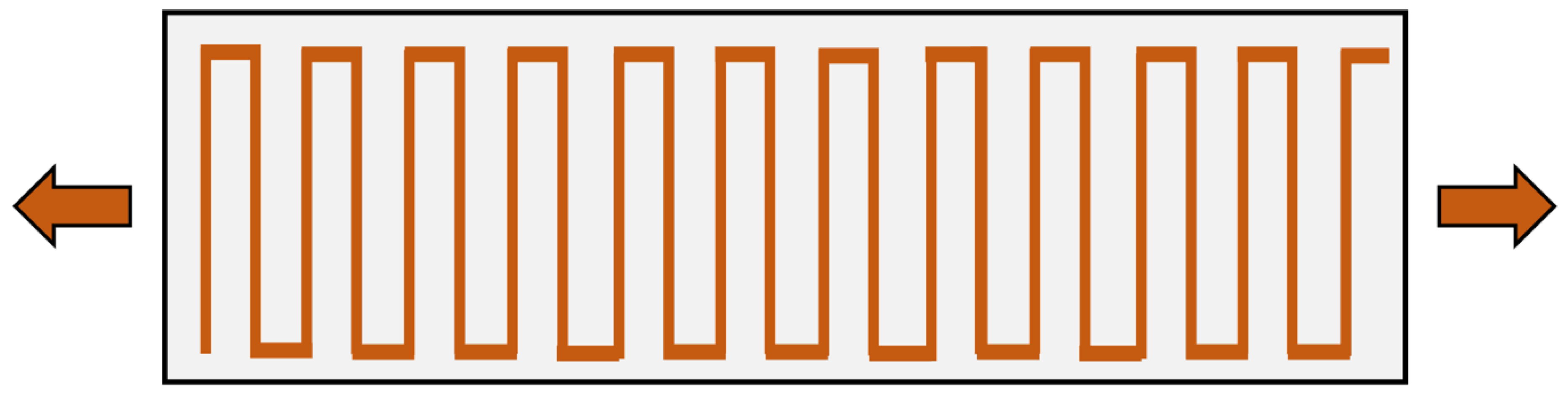
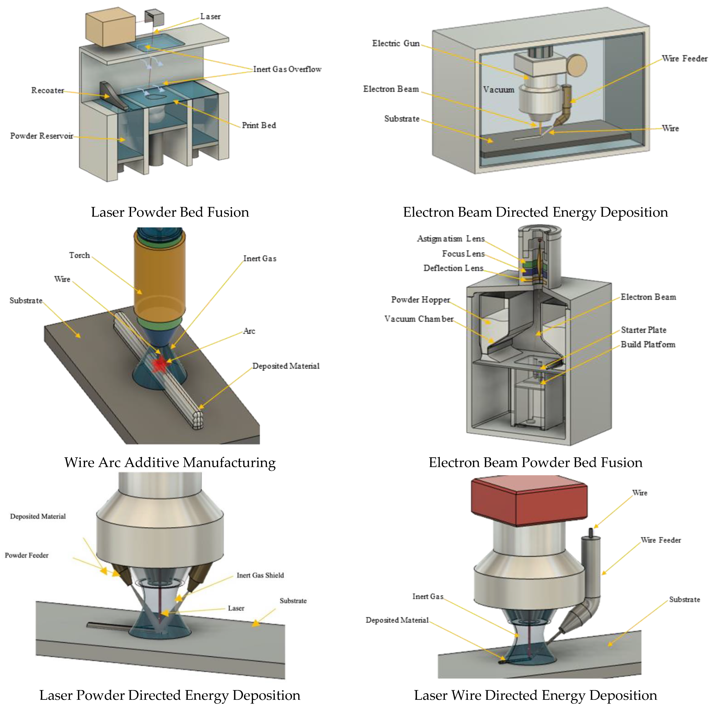
2.1. AM Processes and Processing Parameters

This study involves 6 different AM techniques, or processes, utilizing wire or powder feedstock. These include laser powder bed fusion (L-PBF), electron beam directed energy deposition (EB-DED), wire arc additive manufacturing (WAAM) (or Arc Wire DED), electron beam powder bed fusion (EB-PBF), laser powder directed energy deposition (LP-DED), and laser wire directed energy deposition (LW-DED). These processes are illustrated generally in Figure 1 It is observed that three processes involve wire feed, while three processes involve powder feed or a powder bed. All but the WAAM process utilize electron or laser beam energy sources. Gamon et al. [18] have briefly discussed these process techniques in more detail and trade and selection is discussed in a robust paper from Gradl et al. [19].
Multiple specimens representing the six AM processes (L-PBF, WAAM, EB-DED, LP-DED, EB-PBF, and LW-DED) investigated in this study were evaluated and tested. The parameters used to build each sample are provided in Table 1. In Table 2, an index of each sample is provided, along with a description of the geometries of the as-built specimens. For the LP-DED and LW-DED, different specimens were created to observe any change in microstructure or mechanical property between the varying parameters. The LP-DED had the same build toolpath approach but varied the spot size and subsequent power (from 350 W to 2620 W) and powder feed rate for this study. The coupons’ build varied based on parameters; small coupons were printed with the finest parameters, while faster parameters deposited blocks in order to be more representative of builds using those parameters. The LW-DED samples had a variation only in the tool path used in the build. For example, the raster 90 tool path is angled 90° from the x-axis of the build table; Figure 2 shows this tool path. Raster is a 0° raster tool path and the linear sample follows a path around the perimeter with a 45° infill.
Table 1 compares the primary build parameters for the AM processes utilized in this study (Figure 2). Only the WAAM process utilizes electrical arc parameters (voltage, amperage, wire feedrate), which are not readily comparable. Generally, laser and electron beam melting involve beam power, P, or power density, Q, in Watts, where Q~P/v; and v is the beam travel or scan speed in mm/s (Table 1). For most metals and alloys involved in laser or electron beam processes (Figure 2), the as-built microstructure depends on the so-called temperature gradient, G, and the solidification growth rate, R, where the layer cooling rate is correspondingly expressed as G × R~eaQ; and a is a constant [20]. It is also generally observed that increasing cooling rates (G × R) promote a decreasing microstructure size. Additionally, decreasing G/R promotes columnar-to-equiaxed grain structures in the as-built products [20]. Table 1 illustrates that a range of processing power ranging from 350 to 2620 Watts was selected for the LP-DED AM processing. While Table 1 shows the powder size range and wire diameter for specific AM machines utilized in this study, Table 2 shows the residual specimen or sample geometries with identification coding (sample ID), along with etching times for metallographic specimen preparation.
For this study, all of the samples represented in Table 1 and Table 2 were fully heat-treated. The heat treatment process involved stress relieving (SR) at 1066 °C for 1.5 h, HIP at 1163 °C for 3 to 4 h in inert gas at 100 MPa pressure (per ASTM 3301-18a standard), followed by solution annealing treatment (SOL) at 1177 °C for 1 h, with furnace cooling per AMS 7000/AMS 2774 standard (SR + HIP + SOL).

2.2. Metallographic Preparation

The build direction microstructure was revealed by sectioning as-built samples with an ATM Brilliant 220 precision cutter. To avoid incorrect interpretation of micrographs and material characteristics, samples having a substrate of different material were sectioned and studied at an apparent distance away from the fusion zone from the build plate. Metallographic samples of the sectioned specimens were created using a combination of powdered epoxy and phenolic acid and a hot mounting press from ATM OPAL (Haan, Germany). Grinding and polishing were completed after the samples were mounted to produce a mirror-like surface.
The grinding and polishing procedures were conducted with an ATM SAPHIR 530 semi-automatic system. The grinding procedure started with a 240-grit coarse Si-C (Silicon carbide) grinding paper, followed by grits 320, 400, 600, and 800; each was spun at 300 RPM with a force of 25 N for 1 min, using water as a lubricant. The polishing procedure was carried out at a speed of 150 RPM and a force of 25 N for 5 min, with each stage of the polishing process having a different nylon disk for the 6 µm, 3 µm, and 1 µm diamond slurries. Finally, the samples were polished for 2 min at 150 RPM with a force of 35 N, using a short synthetic nap disk and a 0.5 µm AlO2 (Alumina) slurry. The samples were ultrasonicated prior to polishing and in between each polishing stage to eliminate cross-contamination.
The etchant was a variation of ASTM E407 etchant 149. The solution consisted of 25 mL of hydrochloric acid, 15 mL lactic acid, and 3 mL of hydrogen peroxide. Submersion of the specimens in the etching solution for a range of 45 to 90 s was the etching procedure in this investigation. The optical micrographs in this work were taken with an Olympus GX53 inverted optical microscope (Olympus Inc., Tokyo, Japan).

2.3. Density Measurements

The density measurements were made by using gas displacement pycnometry with a Micromeritics AccuPyc II 1340 for volume measurements and a Sartorius balance system for weight.

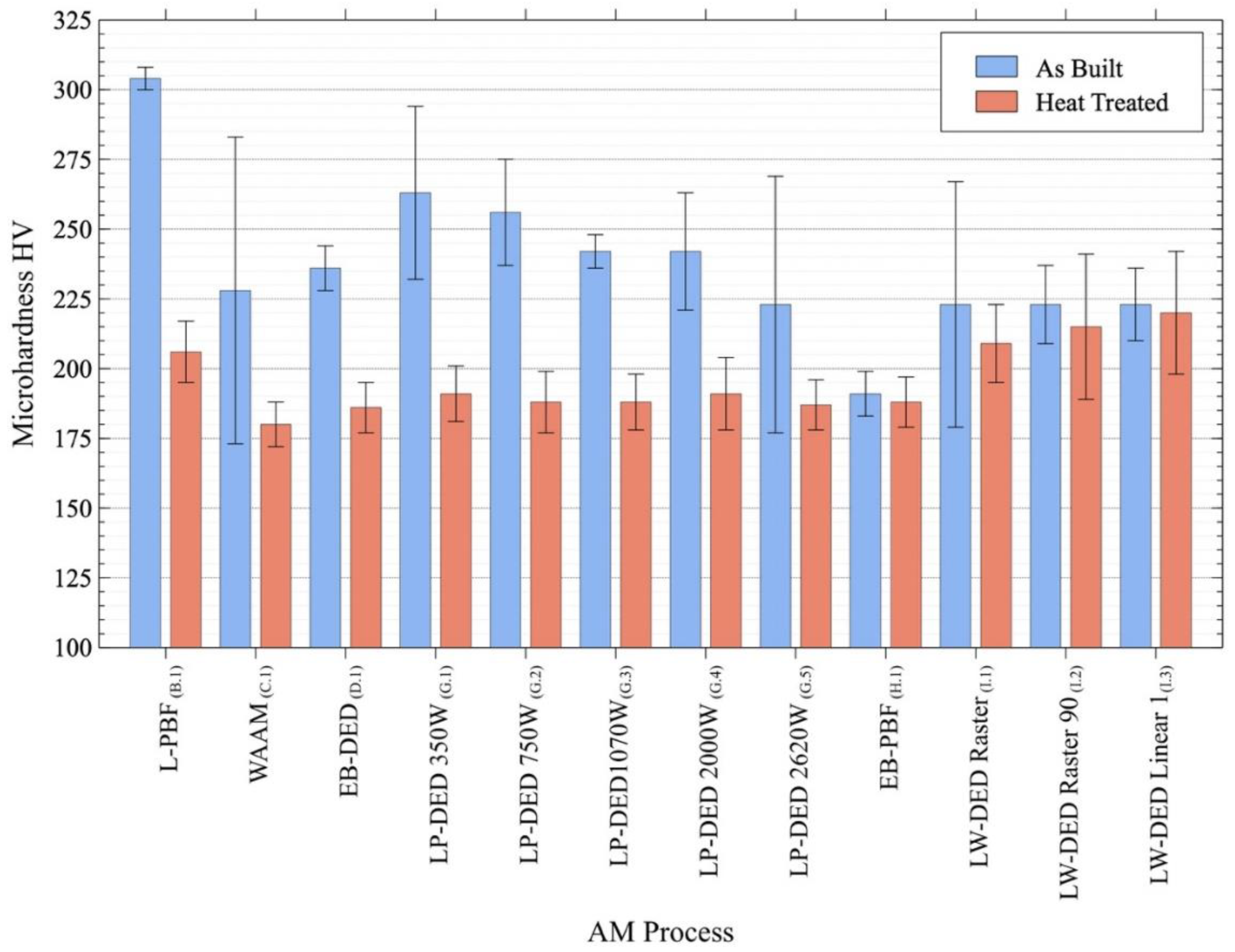
2.4. Hardness Testing

Microindentation hardness was measured at the NASA Marshall Space Flight Center with a Struers Durascan indenter. Indentations were made with a Vickers indenter and a load of 300 gf, and measured with a 50× objective lens. A minimum of ten measurements were taken for each AM process sample.

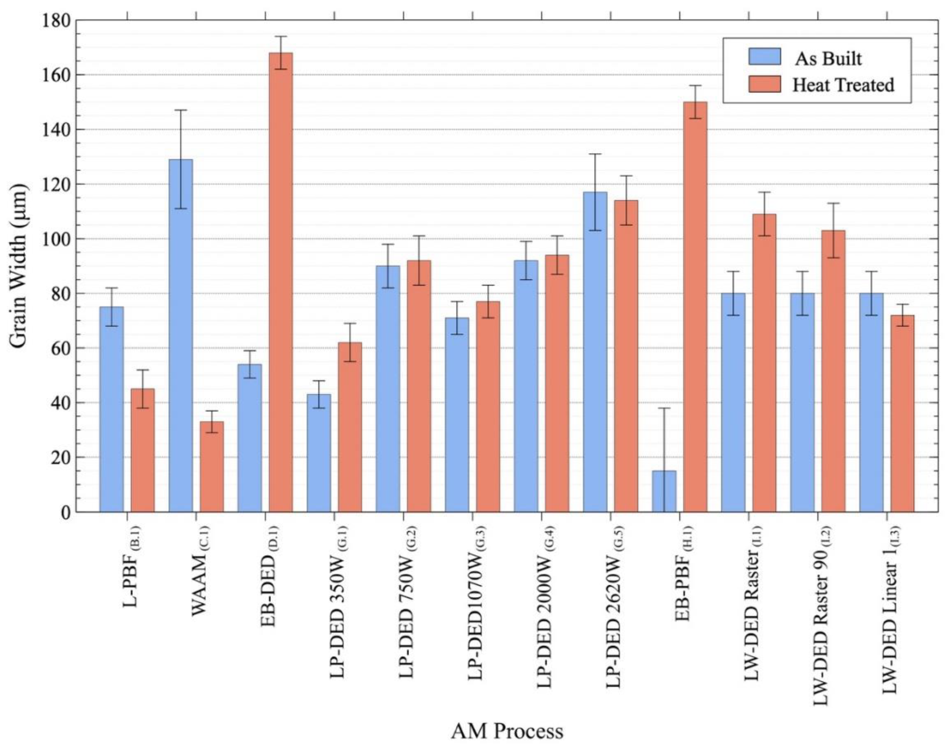
2.5. Grain Width/Size Measurements

The line intercept technique, as published in ASTM E112, was used to conduct grain width measurement. The freeware ImageJ was used to draw and measure straight lines across the micrograph. The number of grain boundaries intercepted was counted until at least 100 grain boundaries were intercepted, per standard procedures [21]. Since etching only showed the dendrite ends, these measurements were frequently supplemented by hand measurements of interdendritic spacings.

2.6. Tensile Tests

Room-temperature tensile testing of the specimens was conducted at Westmoreland Mechanical Testing & Research, Inc. Youngstown, PA, USA, according to ASTM E8-21. All samples were fully machined with a 6.25 mm diameter gage section (measured using calipers) and 4D length of 25.4 mm. An external extensometer was used for all testing until it reached a limit, and then a cross head was used to determine the final elongation. The rate of testing was 0.005 in./in./min until yield and then 0.05 in./min. The fracture surfaces of select tensile test specimens were examined using scanning electron microscopy (JEOL JMS-IT500 SEM).

3. Results

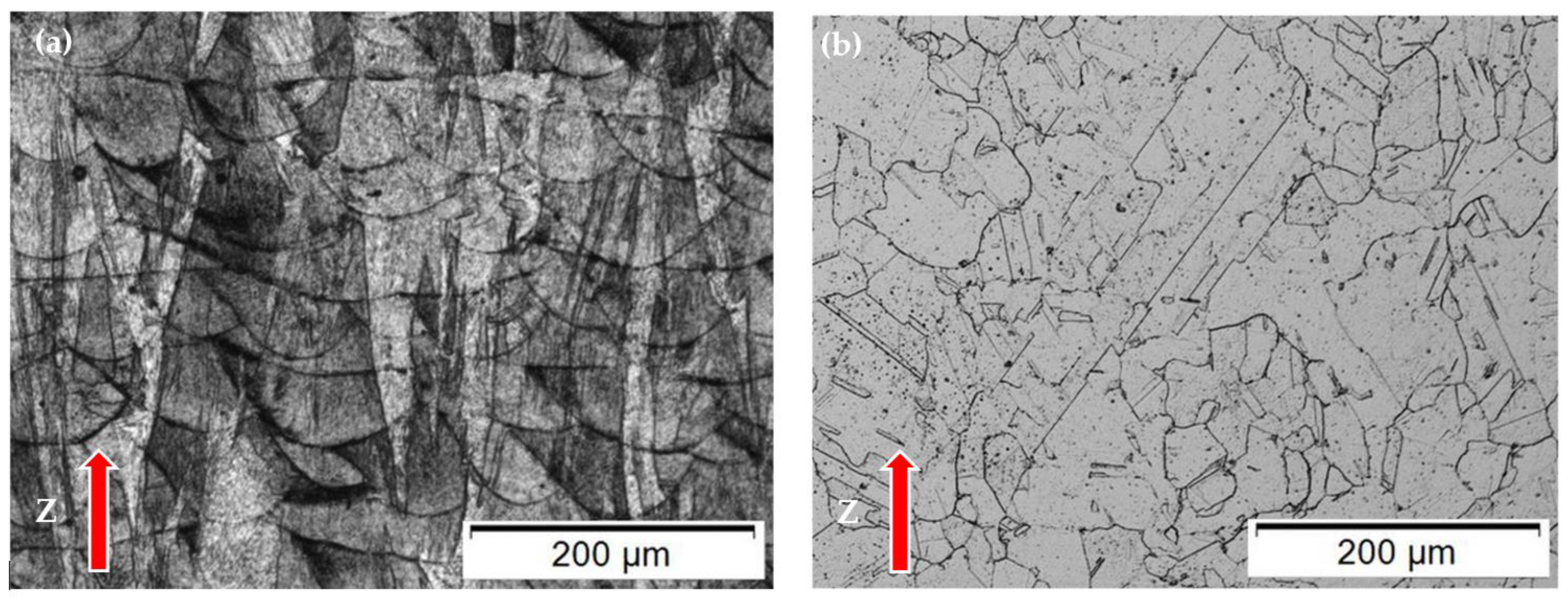
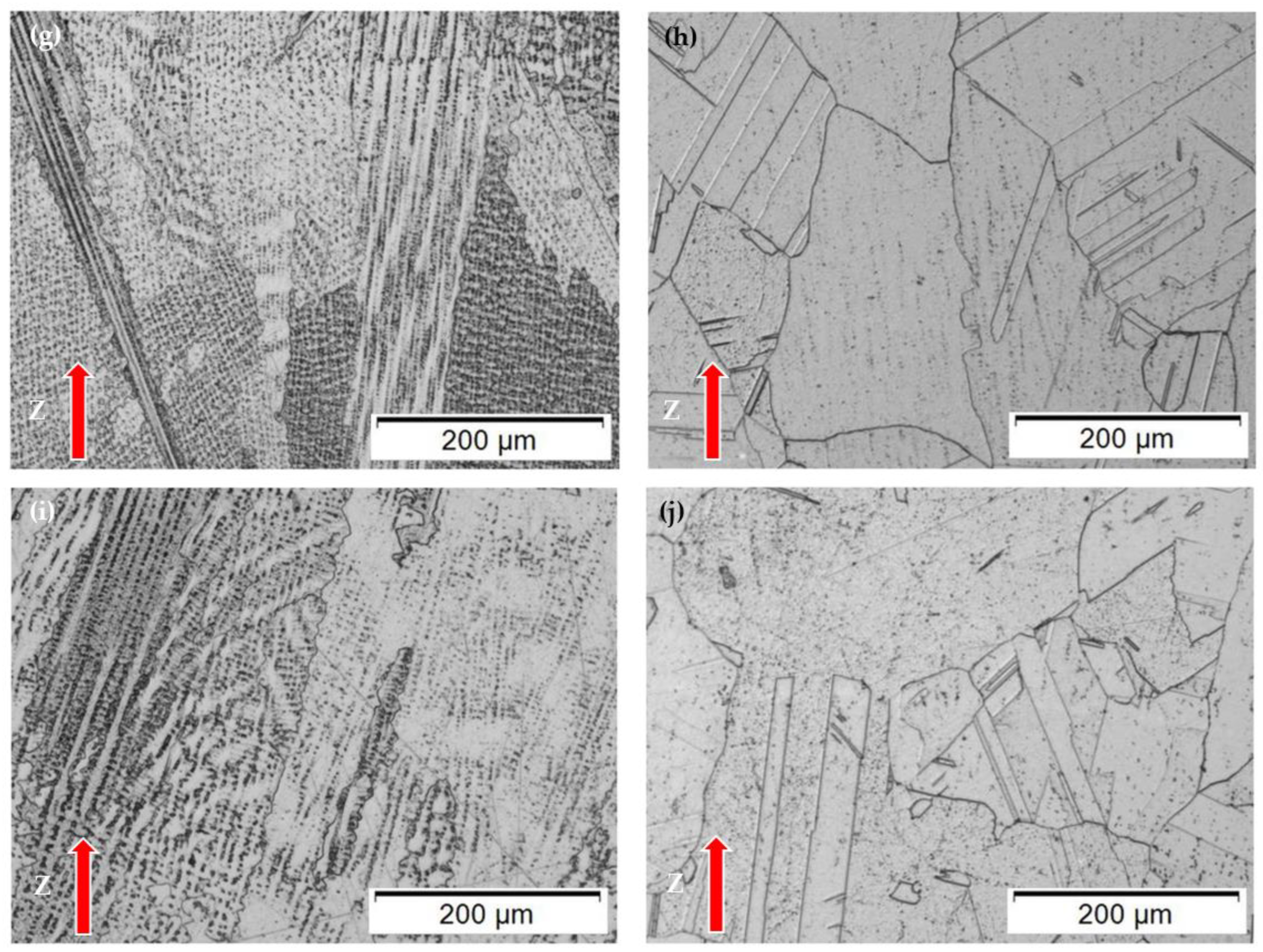
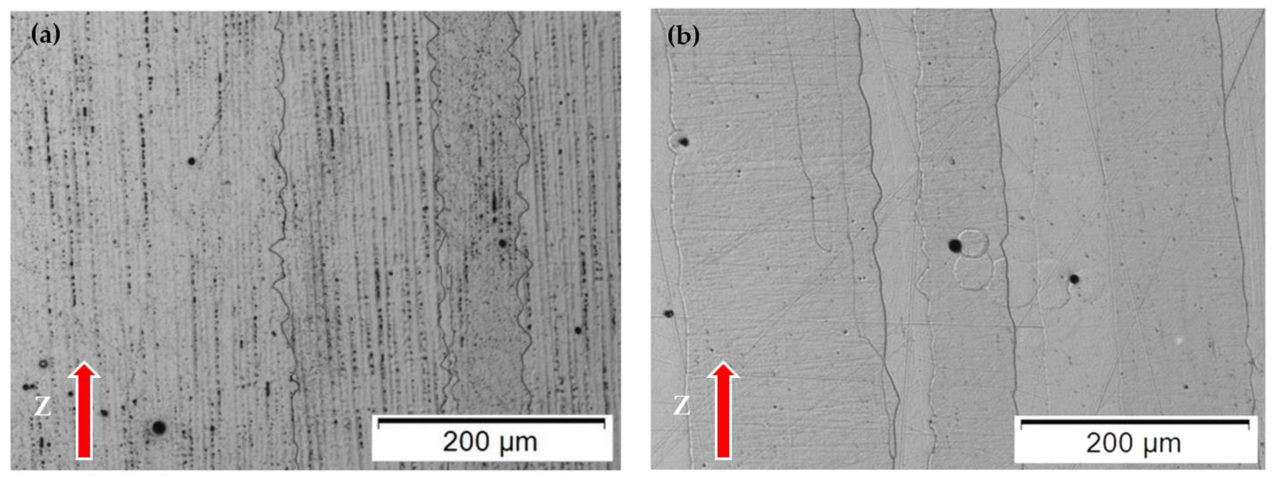
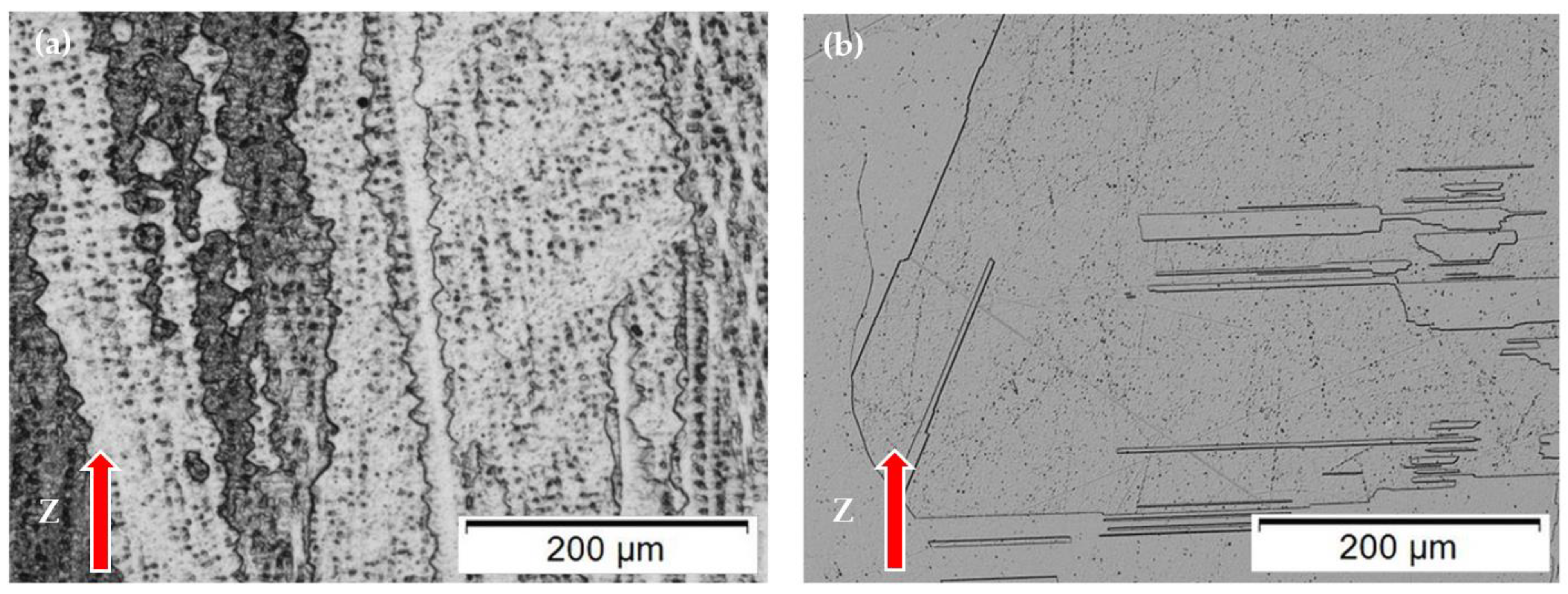
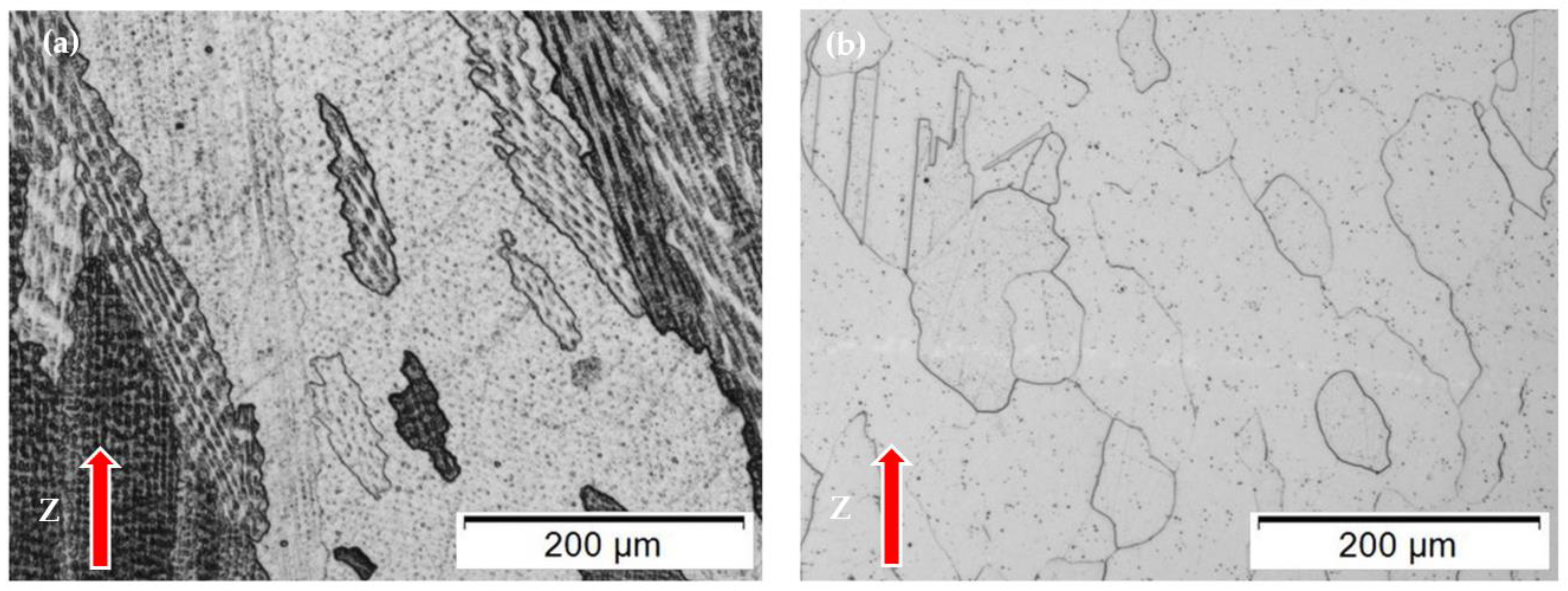
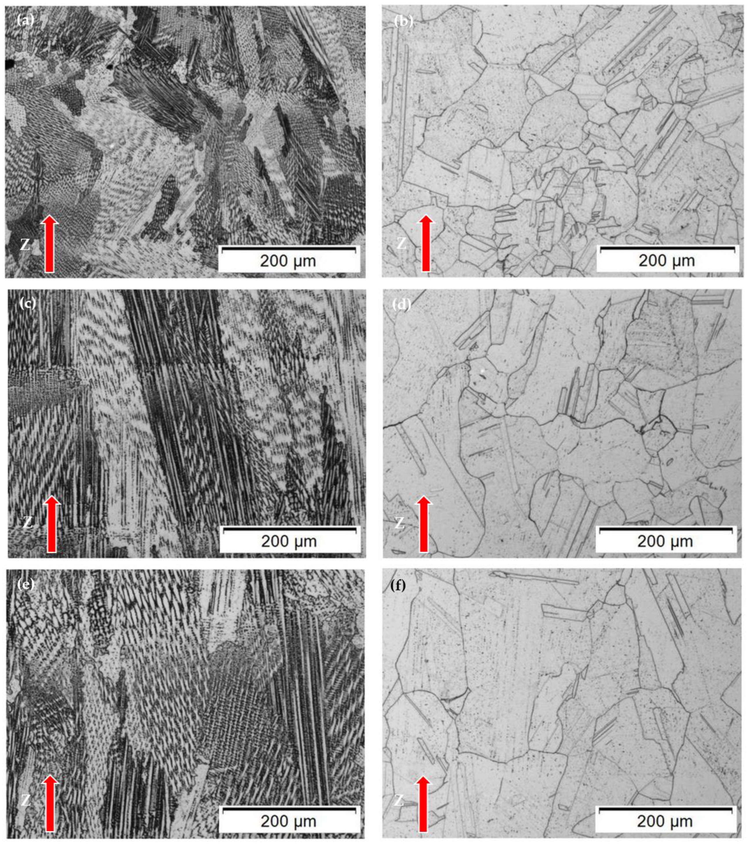
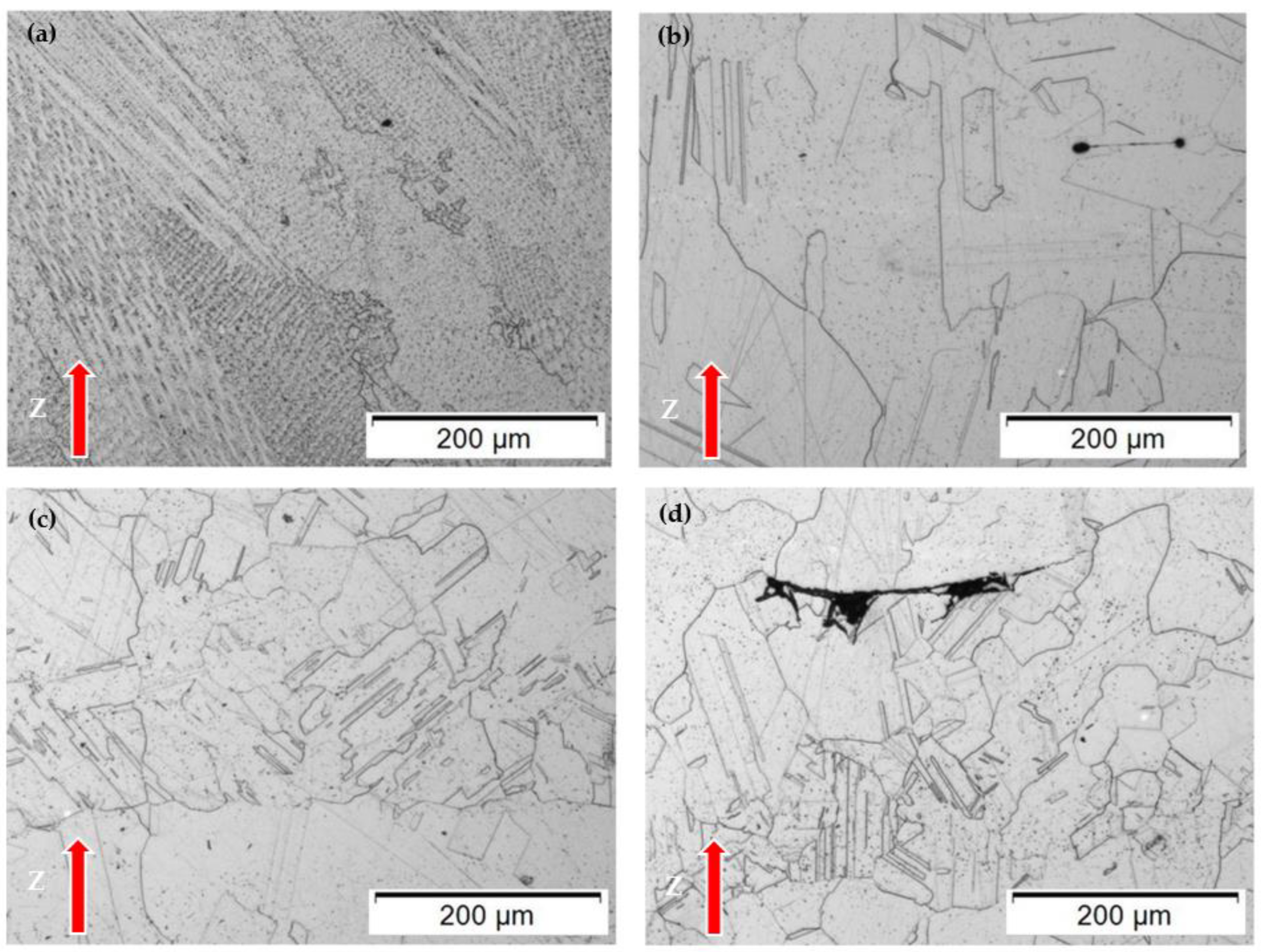
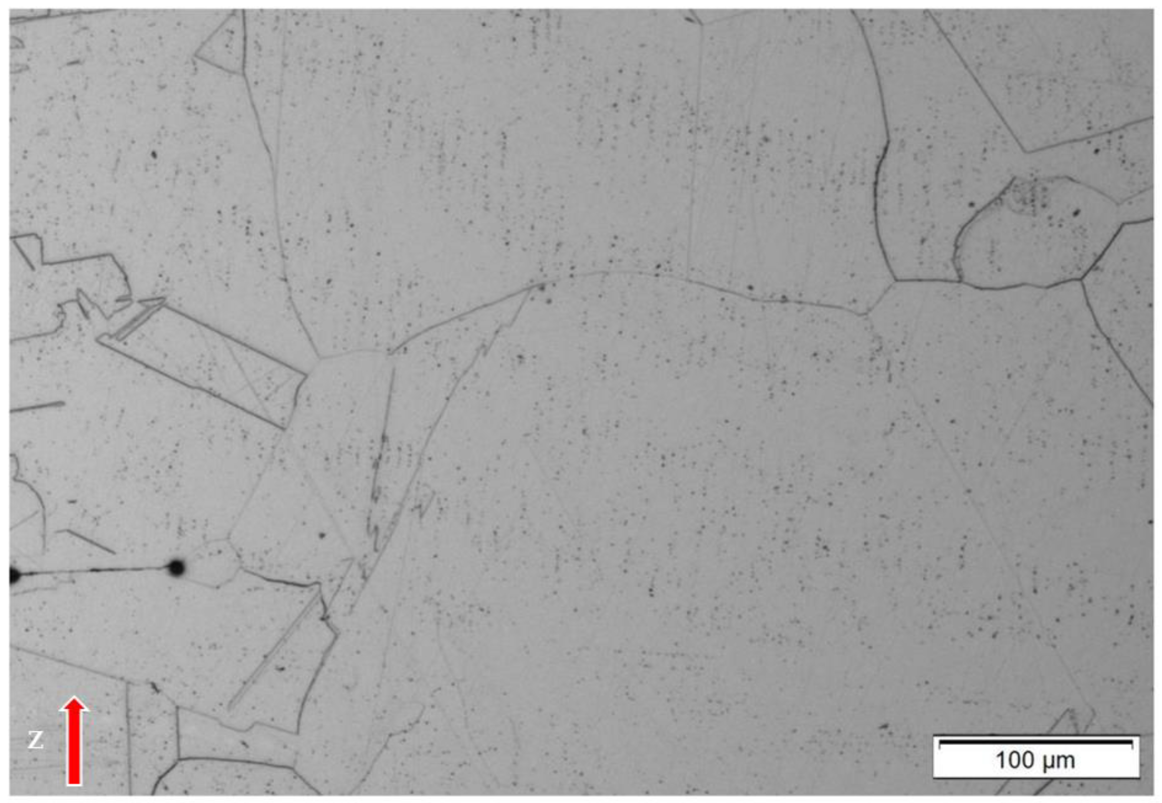
3.1. Microstructures and Microstructure Comparison

Figure 3, Figure 4, Figure 5, Figure 6, Figure 7, Figure 8 and Figure 9 show a very notable difference between the as-built AM process microstructures and those observed for post-process fully heat-treated samples. Essentially, all of the as-built AM process microstructures shown on the left in Figure 3, Figure 4, Figure 5, Figure 6, Figure 7, Figure 8 and Figure 9 exhibit columnar grains of varying lengths and widths, along with various degrees of cellular dendrites and dendritic arrays. The LP-PBF as-built microstructure in Figure 3a also shows the characteristic melt-band structure and overlapping melt pools. Figure 5a and Figure 6a show irregular grain and columnar structures containing cellular dendrites for the EB-DED and LP-DED AM processing, respectively. It is notable that Figure 6 shows the complete range of processing power from 350 W (Figure 6a) to 2620 W (Figure 6j), where only the lower-power LP-DED samples at 350 W (Figure 6a) exhibit a notable, as-built microstructure that is smaller and more irregular than the other processing power samples. Figure 7 and Figure 8 also show fairly regular columnar grains for the as-built samples, with the EB-PBF as-built columns shown in Figure 7a having a grain width averaging 15 microns. The microindentation hardness for the as-built columnar structure in Figure 7a averaged HV 191, in contrast to the as-built L-PBF microstructure in Figure 3a, where the hardness averaged HV 305, and the LW-DED microstructure in Figure 8d, where the hardness averaged HV 224.
By comparison, the post-process heat treatment microstructures shown in Figure 3, Figure 4, Figure 5 and Figure 6 exhibit recrystallized and equiaxed grains of varying widths or sizes, which contain somewhat varying densities of {111} annealing twins, observed as straight interfaces, which are coincident with the traces of fcc {111} planes. The EB-DED heat-treated microstructure shows more irregular grain boundaries, with only a few annealing twins in the upper left corner of Figure 5b. The corresponding microindentation hardness for the heat-treated microstructure in Figure 5b for the EB-DED AM process sample was HV 186, while, in contrast, it was HV 206 for the L-PBF microstructure in Figure 3b and only HV 180 for the WAAM microstructure in Figure 4b, where the grain width averaged 216 microns, in contrast to that for the L-PBF microstructure in Figure 3b, which was 45 microns. This microindentation hardness difference between the heat-treated L-PBF and WAAM microstructures is consistent with the grain size difference: decreasing grain size and correspondingly increasing hardness. This feature was also observed for the LP-DED process series shown in Figure 6, where the 350 W power sample after heat treatment had a grain width/size of 62 microns and a hardness of HV 191 (Figure 6b), in contrast to the 2620 W power sample in Figure 6j, with a grain size of 114 microns and a hardness of HV 187. An exception to this trend is the AM-processed EB-PBF sample in Figure 7, where the as-built columnar grain width is 15 microns, in contrast to the heat-treated specimen columnar grain width of ~150 microns—each having the same microindentation hardness of HV 191. The trend of increasing hardness with decreasing grain size is, however, followed for the LW-DED AM process series shown in Figure 8, where the heat-treated raster grain size in Figure 8b of 9 microns and a hardness of HV 209 is in contrast to the linear 1 grain size in Figure 8d of HV 72 and a corresponding hardness of HV 220.
It is apparent that the high-temperature heat treatment >1100 °C dominated the microstructure development to produce recrystallized, equiaxed grain structures, or widened columnar grain widths in the case of the EB-PBF sample in Figure 7b. In addition to the varying densities of annealing twins in the recrystallized grains, they also show second-phase particles, presumably carbides, which appear as black dots on close investigation. This feature is more apparent in the magnified view of the heat-treated LW-DED raster sample shown in Figure 9.
It is observed that there are no particles on the straight {111} coincident annealing twin boundaries. This is a well-established phenomenon that results from the very low interfacial free energy for the twin boundaries in contrast to the grain boundaries [22,23]. A similar observation has been made for AM-processed and heat-treated Inconel 690 [24]. It is also noted that the twin boundary widths and their partitioning of the grains were not included in the grain width measurements. Consequently, there may be a contribution to further grain partitioning, which could have a small contribution to the hardness. In this regard, there seems to be no notable contribution of the particles to the hardness, even though the average interparticle spacing is between 1 and 2 microns.
It has been noted that in alloys such as 304 stainless steel and Inconel 690, the presence of {111} coincident annealing twin boundaries in the grain structure improves the corrosion resistance as a consequence of their low interfacial energy relative to the grain boundaries, as noted above [22,23,25]. It is not clear in this study that there are sufficient numbers of annealing twins to affect this property. However, future studies to examine this issue may prove to be valuable, especially for corrosive environment applications.
It is also worth noting that in Figure 7 and Figure 8, there is evidence of porosity and lack of fusion (LoF) regions, respectively. The density for the as-built EB-PBF sample was the lowest at 99.1%, which improved to 99.9% after full heat treatment, driven by the HIP. However, Figure 7 illustrates some porosity even after HIP. The heat-treated raster 1 LW-DED sample in Figure 8d also shows a region of LoF, where the density was measured to be 99.5%, compared with 99.9% for the as-built specimen.

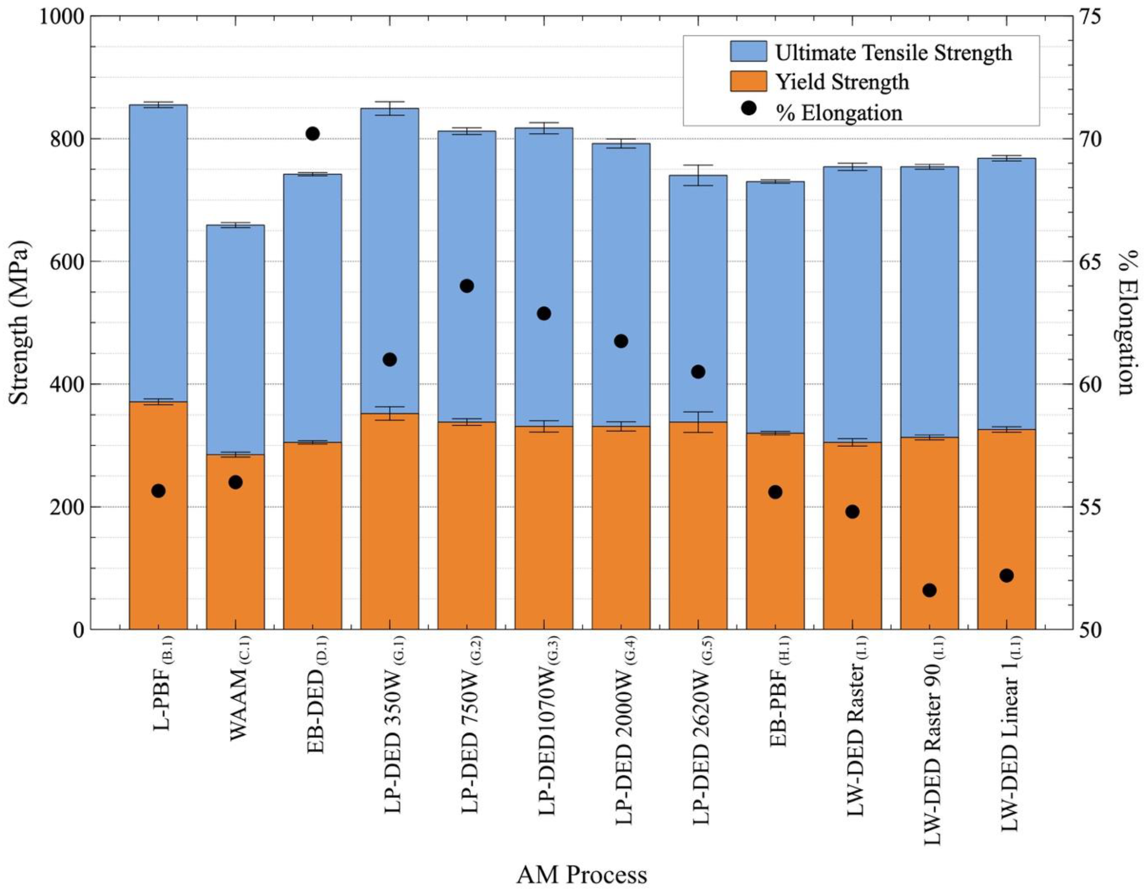
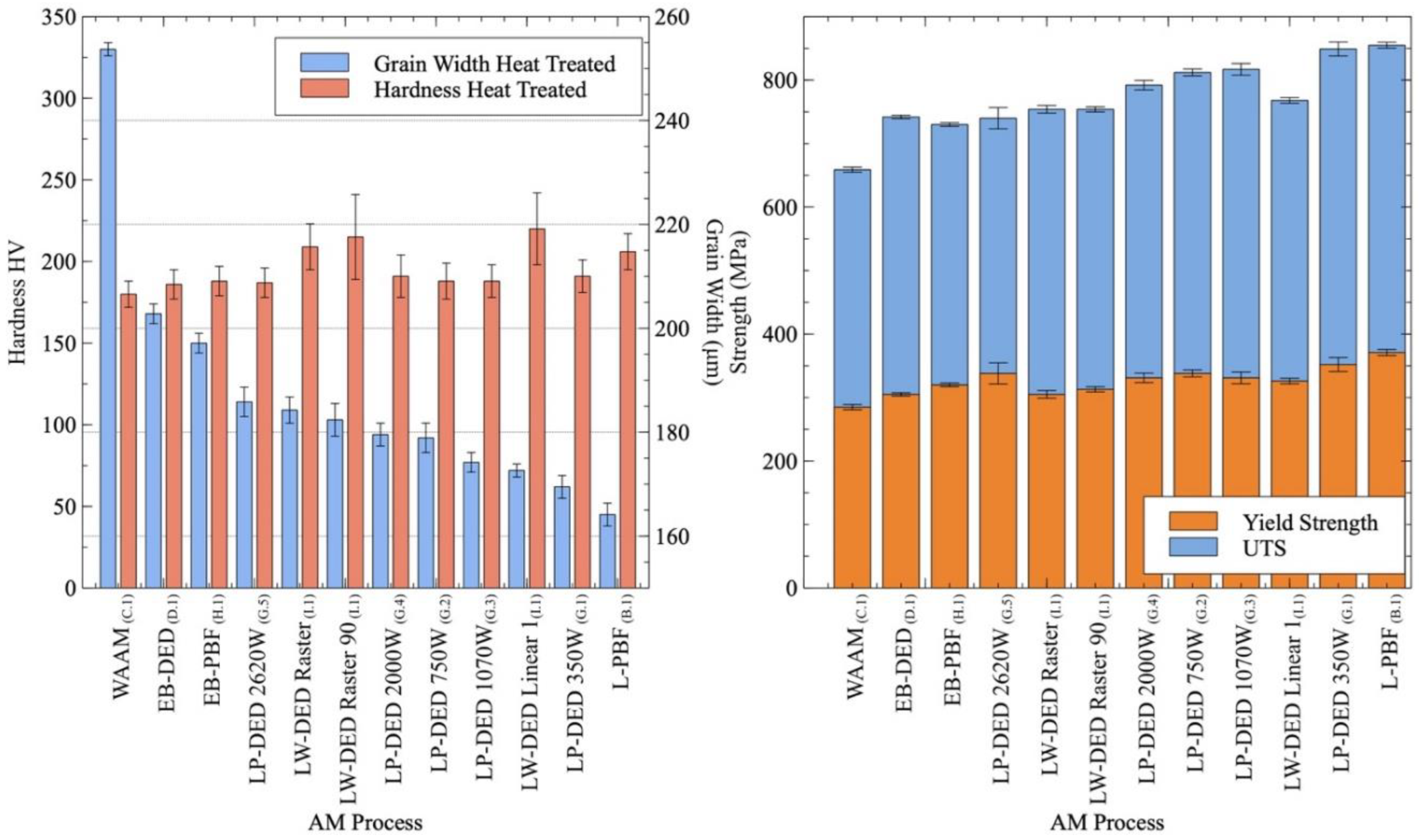
3.2. Microstructure and Mechanical Property Comparisons and Discussion

Table 2 and Table 3 list and summarize the as-built and fully heat-treated Inconel 625 AM process sample properties, including residual densities, grain morphologies and nominal grain widths, Vickers microindentation hardness (HV), and tensile properties (yield stress, UTS, and elongation (%)) in the case of the heat-treated samples listed in Table 3. Complementing these tables, Figure 10 and Figure 11 show comparative bar graphs for the average grain widths and microhardness measurements, respectively, for as-built and fully SR + HIP + SOL heat-treated AM process samples, utilizing the data in Table 3. A notable feature in Figure 10 and Figure 11 is the generally increasing hardness with decreasing grain width. This relationship is shown in Figure 12 where the heat treated samples are placed in order of decreasing grain width with the corresponding microhardness. The summary of ultimate tensile strength and yield strength in the same order is included in this figure.
Figure 13 shows little change in the yield stress and UTS over the range of heat-treated AM process samples, with the exception of the WAAM and EB-DED products, which exhibit the largest grain widths. The EB-DED heat-treated sample also shows the largest elongation of 70.2% (Table 3). While the heat treatment of the various AM processes varied from HV 191 to HV 220 (Table 3)—a variance of 15%—the as-built variance was HV 191 to HV 304, or 59%. The corresponding as-built yield strength varied from 285 MPa for the heat-treated WAAM sample to 371 MPa for the L-PBF sample, a variance of 30% (Table 3). The corresponding elongations for the heat-treated AM process samples varied from a low of ~52% to a high of ~70%, as noted above—a variance of 35% (Table 3). These features are generally consistent with a wide window for mechanical property manipulation for the heat treatment of a variety of AM processes, as presented in Figure 2.
As noted above, the high temperatures associated with the current heat treatment of variously produced AM process samples dominated the residual microstructure production, forming recrystallized grains containing annealing twins and carbide precipitates, neither of which seemed to have a significant effect on the residual mechanical properties. Recrystallization and the resulting grain growth have the advantage of eliminating anisotropy in laser powder bed fusion-produced Inconel 625 alloy [26].

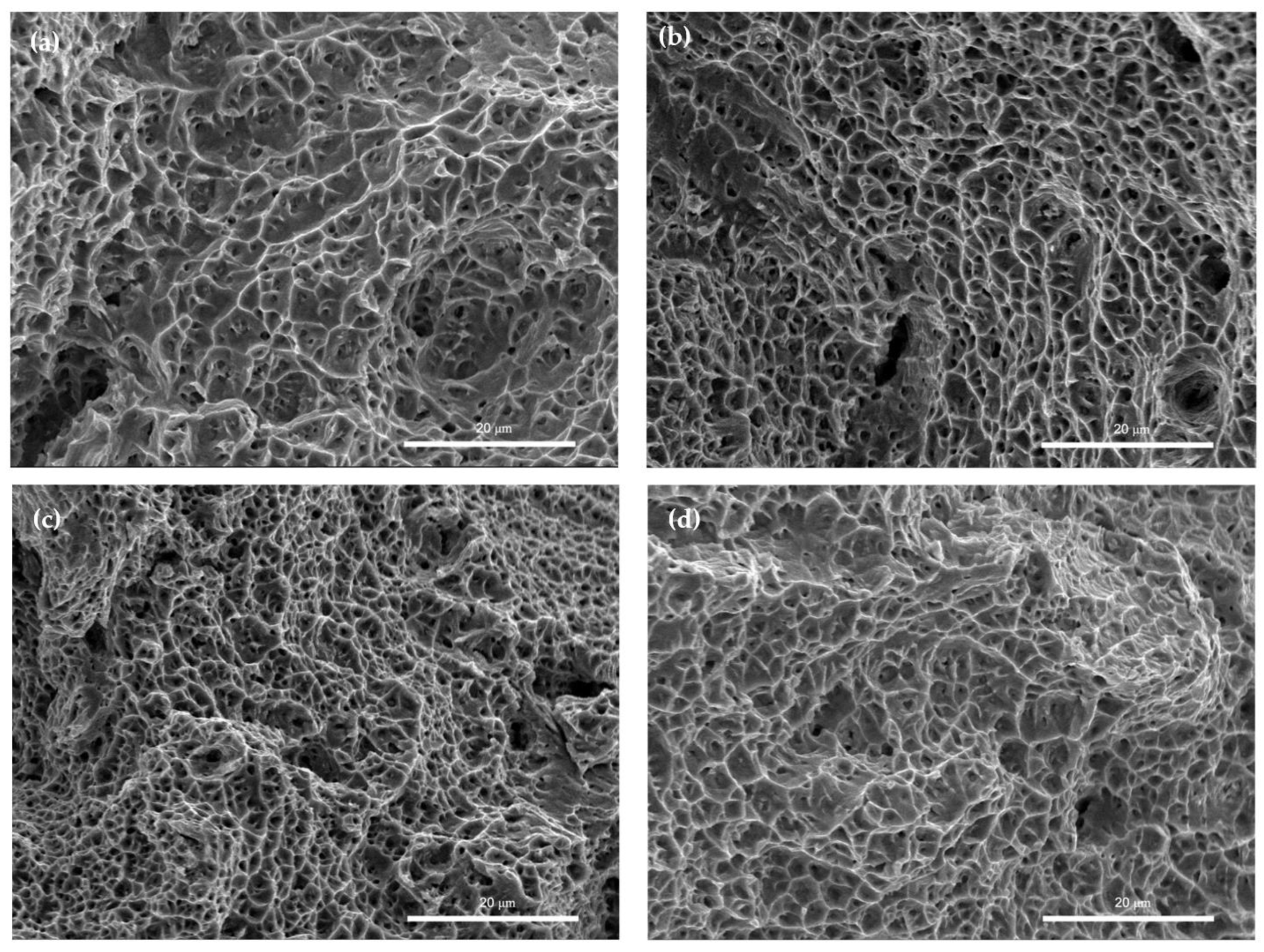
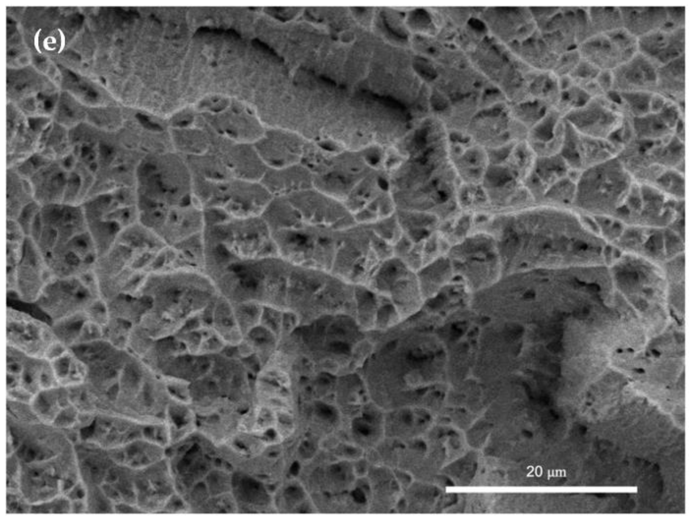
3.3. Fracture Surface Observations and Discussions

SEM images showing fracture surface features for the heat-treated, AM-processed samples generally exhibited ductile dimples having dimple sizes ranging from 2 to 5 microns. The largest dimple sizes of ~5 microns were observed for the WAAM heat-treated samples, while the smallest sizes were observed for the EB-PBF and LP-DED fractured samples. Figure 14 illustrates these ductile dimple fracture features for the LP-DED AM process heat-treated sample series, using build power levels ranging from 350 W to 2620 W. In Figure 14a, the dimple size is ~2 microns (at 350 W), while the remaining fracture dimple sizes are ~3–4 microns. These features are consistent with corresponding grain width variations and the associated yield strength, e.g., 62 microns and 354 MPa at 350 W (Figure 14a) versus 114 microns and 336 MPa at 2620 W (Figure 14e). These dimple sizes and corresponding grain sizes (widths), and yield stresses, are generally consistent with trends in a range of metal and alloy fractures where dimple size decreases with decreasing grain size and yield stress [27,28].
What is not necessarily consistent in these fracture ductile dimple size differences is the generally high elongation, which, from Table 3, varies from a low of ~61% to ~64% for the LP-DED fracture surface series in Figure 14. In fact, the generally high elongations for all heat-treated samples in Table 3 are somewhat unusual since the variation in yield stresses from 285 MPa for the WAAM heat-treated components to 371 MPa for the L-PBF components shows essentially the same elongation of ~56%.

4. Summary and Conclusions

A comprehensive study was provided to compare the as-built and fully heat-treated (SR + HIP + SOL) microstructure and resulting mechanical properties across various metal AM processes using Alloy 625 (Inconel 625). It is shown that various metal AM processes (Figure 1) can provide a range of residual, as-built properties, which can be selectively enhanced or manipulated by the sequence of heat treatment (SR + HIP + SOL). This study has provided a wide, comparative overview for Inconel 625 alloy product development and application optimization, especially focused on mechanical properties: hardness and tensile. While wrought and cast Inconel 625 products can have hardness values ranging from ~HV 180 to HV 320 after lower-temperature aging (<700 °C), corresponding to yield stress values ranging from 290 MPa (with elongations of ~65%) to ~900 MPa (with elongations of ~31%), AM processing and post-process heat treatments of Inconel 625 can produce a similar range of mechanical properties—with various AM processes providing a window of selection for optimizing specific applications. This study employed a range of six AM processes (and various parameters) and compared the properties of as-built samples and high-temperature heat treatments (SR + HIP + SOL) of these samples. The as-built samples showed a microindentation hardness range of ~HV 191 to HV 304, while the heat-treated sample hardnesses ranged from HV 186 to HV 220. Yield stresses for the heat-treated samples ranged from 285 MPa with 56% elongation to 371 MPa with the same elongation.
High-temperature heat treatment >1100 °C in this study provided a fairly uniform degree of homogenization of the microstructure as a result of the recrystallization of the as-built microstructures. The resulting, equiaxed grain structure for all but the EB-PBF products contained {111} fcc annealing twins, which might be further optimized to provide enhanced corrosion resistance, which has been observed for numerous other alloys, including superalloys [22,23,24,25].
In general, the important conclusions of this study include the following:
  • A wide variety of AM process-built Inconel 625 products can be heat-treated at high temperatures >1100 °C to produce desirable and optimal mechanical properties for specialized application optimization through mostly homogeneous, recrystallized, equiaxed grain structures containing annealing twin boundaries. The sequence—including stress relief, HIP, and solution—must be performed to obtain the desired mechanical properties.
  • Equiaxed and twinned grain structures produced by high-temperature (>1100 °C) heat treatment of various AM process components might be further engineered to provide more dense twin boundaries, which could result in enhanced corrosion resistance.
  • AM processes such as WAAM, which invest large amounts of energy (heat) into the build, have limited and low values of residual mechanical properties, including hardness, which is not significantly improved or altered with high-temperature heat treatment.
  • For LP-DED as-built products having process power ranging from 350 W to 2620 W, Vickers microindentation hardness varied from HV 263 to HV 223, respectively, while the heat-treated samples’ hardness varied from HV 191 to HV 187, respectively—a variance of only 2%.

Author Contributions

Conceptualization, V.L., L.T., A.G., E.A., P.R.G. and F.M.; data curation, V.L., L.T., A.G., C.K. and P.R.G.; investigation, V.L., L.T., A.G., E.A., P.R.G. and F.M.; resources, C.K., P.R.G. and F.M.; supervision, P.R.G. and F.M.; visualization, V.L., L.T., A.G., E.A., C.K., P.R.G. and F.M.; writing—original draft, V.L., L.T., A.G., E.A., L.E.M., C.K., P.R.G. and F.M.; writing—review and editing, V.L., L.T., A.G., E.A., L.E.M., R.B.W., C.K., P.R.G. and F.M. All authors have read and agreed to the published version of the manuscript.

Funding

This research was funded under NASA contract 80NSSC22PA055 and support was provided by in-house funding at the NASA Marshall Space Flight Center.

Data Availability Statement

Not applicable.

Acknowledgments

Thank you to partners providing samples, including Visser Precision, GE Research, Keystone Synergistic, RPM Innovations, Lincoln Electric, NASA Langley Research Center, ExOne.

Conflicts of Interest

The authors declare no conflict of interest. This paper describes objective technical results and analysis. Any subjective views or opinions that might be expressed in the paper do not necessarily represent the views of the National Aeronautics and Space Administration (NASA) or the United States Government. The results from this study are solely for informational purposes and not an endorsement of any techniques by the authors, their employers, or the publishing journal.

References

  1. Floreen, S.; Fuchs, G.F.; Yang, W.J. Metallurgy of Alloy 625, Superalloys 718, 625 and Various Derivatives; Loria, E.A., Ed.; The Minerals, Metals and Materials Society: Warrendale, PA, USA, 2007; pp. 13–37. [Google Scholar]
  2. Shankar, V.; Rao, K.B.S.; Mannan, S. Microstructure and mechanical properties of Inconel 625 superalloy. J. Nucl. Mater. 2001, 288, 222–232. [Google Scholar] [CrossRef]
  3. Shoemaker, L.E. Alloys 625 and 725: Trends in Properties and Applications, Superalloys 718, 625 and Various Derivatives; Loria, E.A., Ed.; The Minerals, Metals and Materials Society: Warrendale, PA, USA, 2005; pp. 409–418. [Google Scholar]
  4. Amato, K.N.; Hernandez, J.; Murr, L.E.; Martinez, E.; Gaytan, S.M.; Shindo, P.W. Comparison of microstructures and properties for a nickel-base superalloy (625) fabricated by electron and laser beam melting. J. Mater. Sci. Res. 2012, 1, 3. [Google Scholar]
  5. Marchese, G.; Lorusso, M.; Parizia, S.; Bassini, E.; Lee, J.-W.; Calignano, F.; Manfredi, D.; Terner, M.; Hong, H.-U.; Ugues, D.; et al. Influence of heat treatments on microstructure evolution and mechanical properties of Inconel 625 processed by laser powder bed fusion. Mater. Sci. Eng. A 2018, 729, 64–75. [Google Scholar] [CrossRef]
  6. Li, C.; White, R.; Fang, X.Y.; Weaver, M.; Guo, Y.B. Microstructure evolution characteristics of Inconel 625 alloy from selective laser melting to heat treatment. Mater. Sci. Eng. A 2017, 705, 20–31. [Google Scholar] [CrossRef]
  7. Blakey-Milner, B.; Gradl, P.; Snedden, G.; Brooks, M.; Pitot, J.; Lopez, E.; Leary, M.; Berto, F.; du Plessis, A. Metal additive manufacturing in aerospace: A review. Mater. Des. 2021, 209, 110008. [Google Scholar] [CrossRef]
  8. Reed, R.C. The Superalloys: Fundamentals and Applications; Cambridge University Press: New York, NY, USA, 2006. [Google Scholar]
  9. Binczyk, F.; Śleiona, J. Macro- and microhardness if IN-713C nickel superalloy constituents. Arch. Foundry Eng. 2009, 9, 9–12. [Google Scholar]
  10. Singh, A.; Nag, S.; Chattopadhyay, S.; Ren, Y.; Tiley, J.; Viswanathan, G.; Fraser, H.; Banerjee, R. Mechanisms related to different generations of γ′ precipitation during continuous cooling of a nickel base superalloy. Acta Mater. 2012, 61, 280–293. [Google Scholar] [CrossRef]
  11. Zhang, D.Y.; Niu, W.; Cao, X.Y.; Liu, Z. Effect of standard heat treat on the microstructure and mechanical properties of selective laser melting manufactured Inconel 718 superalloy. Mater. Sci. Eng. A 2015, 644, 32. [Google Scholar] [CrossRef]
  12. Tucho, W.M.; Cuvillier, P.; Sjolyst-Kverneland, A.; Hansen, V. Microstructure and hardness studies of Inconel 718 manufactured by selective laser melting before and after solution heat treatment. Mater. Sci. Eng. A 2017, 689, 220–232. [Google Scholar] [CrossRef]
  13. Chlebus, E.; Gruber, K.; Kuźnicka, B.; Kurzac, J.; Kurzynowski, T. Effect of heat treatment on the microstructure and mechanical properties of Inconel 718 processed by selective laser melting. Mater. Sci. Eng. A 2015, 639, 647–655. [Google Scholar] [CrossRef]
  14. Deng, D.; Moverare, J.; Peng, R.L.; Söderberg, H. Microstructure and anisotropic mechanical properties of EBM manufactured Inconel 718 and effects of post heat treatments. Mater. Sci. Eng. A 2017, 693, 151–163. [Google Scholar] [CrossRef]
  15. Schneider, J.; Lund, B.; Fullen, M. Effect of heat treatment variations on the mechanical properties of Inconel 718 selective laser melted specimens. Addit. Manuf. 2018, 21, 248–254. [Google Scholar] [CrossRef]
  16. Rao, G.A.; Kumar Srinivas, M.; Sarma, D.S. Effect of standard heat treatment on the microstructure and mechanical properties of hot isostatically pressed super alloy Inconel 718. Mater. Sci. Eng. A 2003, 355, 114. [Google Scholar] [CrossRef]
  17. Raghavan, S.; Zhang, B.C.; Wang, P.; Sun, C.N.; Nai, M.L.S.; Li, T.; Wei, J. Effect of different heat treatments on the microstructure and mechanical properties in selective laser melted INCONEL 718 alloy. Mater. Manuf. Processes 2017, 32, 1588. [Google Scholar] [CrossRef]
  18. Gamon, A.; Arrieta, E.; Gradl, P.R.; Katsarelis, C.; Murr, L.E.; Wicker, R.B.; Medina, F. Microstructure and hardness comparison of as-built inconel 625 alloy following various additive manufacturing processes. Results Mater. 2021, 12, 100239. [Google Scholar] [CrossRef]
  19. Gradl, P.; Tinker, D.; Park, A.; Mireles, O.; Garcia, M.; Wilkerson, R.; Mckinney, C. Robust metal additive manufacturing process selection and development for aerospace components. J. Mater. Eng. Perform. 2021, 31, 6013–6044. [Google Scholar] [CrossRef]
  20. DebRoy, T.; Wei, H.L.; Zuback, J.S.; Mukherjee, T.; Elmer, J.W.; Milewski, J.O.; Beese, A.M.; Wilson-Heid, A.; De, A.; Zhang, W. Additive manufacturing of metallic components–Process, structure and properties. Prog. Mater. Sci. 2018, 92, 112–224. [Google Scholar] [CrossRef]
  21. Schneider, C.A.; Rasband, W.S.; Eliceiri, K.W. NIH Image to ImageJ: 25 Years of image analysis. Nat. Methods 2012, 9, 671–675. [Google Scholar] [CrossRef]
  22. Murr, L.E. Interfacial Phenomena in Metals and Alloys; Addison-Wesley Publishing Co.: Reading, MA, USA, 1975. [Google Scholar]
  23. Trillo, E.; Murr, L. Effects of carbon content, deformation, and interfacial energetics on carbide precipitation and corrosion sensitization in 304 stainless steel. Acta Mater. 1999, 47, 235–245. [Google Scholar] [CrossRef]
  24. Segura, I.; Murr, L.; Terrazas, C.; Bermudez, D.; Mireles, J.; Injeti, V.; Li, K.; Yu, B.; Misra, R.; Wicker, R. Grain boundary and microstructure engineering of Inconel 690 cladding on stainless-steel 316L using electron-beam powder bed fusion additive manufacturing. J. Mater. Sci. Technol. 2019, 35, 351–367. [Google Scholar] [CrossRef]
  25. West, E.A.; Was, G.S. Grain boundary engineered 316L and 690 in supercritical water. J. Nuclear Mater. 2009, 392, 264–271. [Google Scholar] [CrossRef]
  26. Marchese, G.; Parizia, S.; Rashidi, M.; Saboori, A.; Manfredi, D.; Ugues, D.; Lombardi, M.; Hryha, E.; Biamino, S. The role of texturing and microstructure evolution on the tensile behavior of heat-treated Inconel 625 produced via laser powder bed fusion. Mater. Sci. Eng. A 2020, 769, 138500. [Google Scholar] [CrossRef]
  27. Das, A.; Trafder, S. Geometry of dimples and its correlation with mechanical properties of stainless steel. Scripta Mater. 2008, 59, 1014–1017. [Google Scholar] [CrossRef]
  28. Qin, W.; Li, J.; Liu, Y.; Kang, J.; Zhu, L.; Shu, D.; Peng, P.; She, D.; Meng, D.; Li, Y. Effects of grain size on tensile property and fracture morphology of 316L stainless steel. Mater. Lett. 2019, 254, 116–119. [Google Scholar] [CrossRef]
Figure 1. AM process schematic visualizations for layer-building techniques used in this research.
Jmmp 06 00107 g001
Figure 2. LW-DED Raster 90 toolpath.
Jmmp 06 00107 g002
Figure 3. L-PBF optical microscope images: (a) as-built, (b) heat-treated.
Jmmp 06 00107 g003
Figure 4. WAAM optical microscope images: (a) as-built, (b) heat-treated.
Jmmp 06 00107 g004
Figure 5. EB-DED: (a) as-built, (b) heat-treated.
Jmmp 06 00107 g005
Figure 6. LP-DED optical microscope images: (a) 350 W as-built, (b) 350 W heat-treated, (c) 750 W as-built, (d) 750 W heat-treated, (e) 1070 W as-built, (f) 1070 W heat-treated, (g) 2000 W as-built, (h) 2000 W heat-treated, (i) 2620 W as-built, (j) 2620 W heat-treated.
Jmmp 06 00107 g006aJmmp 06 00107 g006b
Figure 7. EB-PBF optical microscope images: (a) as-built, (b) heat-treated.
Jmmp 06 00107 g007
Figure 8. LW-DED optical microscope images: (a) as-built, (b) heat-treated raster, (c) heat-treated raster 90, (d) heat-treated linear 1.
Jmmp 06 00107 g008
Figure 9. LW-DED raster heat-treated optical microscope image. Higher magnification showing precipitates (dark spots).
Jmmp 06 00107 g009
Figure 10. Direct comparison of AM process grain widths for as-built and heat-treated (stress relief, HIP, solution) components.
Jmmp 06 00107 g010
Figure 11. Comparison of microhardness in the as-built versus fully heat-treated (SR + HIP + SOL) condition for AM processes.
Jmmp 06 00107 g011
Figure 12. Comparison of grain width and microhardness of heat-treated samples ordered by decreasing grain width and summary of ultimate tensile strength and yield strength in the same order.
Jmmp 06 00107 g012
Figure 13. Summary of the ultimate tensile and yield strength of the specimens for heat-treated AM process samples.
Jmmp 06 00107 g013
Figure 14. LP-DED heat-treated SEM fractography images: (a) 350 W, (b) 750 W, (c) 1070 W, (d) 2000 W, (e) 2620 W.
Jmmp 06 00107 g014aJmmp 06 00107 g014b
Table 1. As-built AM process parameters.
SampleMachineType of FeedstockSizePower (W)Travel Speed (mm/s)Feedstock Feed RateLayer Thickness (µm)Sample IDEtchant Time (s)
L-PBFEOS M400-4Powder15–45 µm1801000N/A40B.160 ± 10
WAAMLincoln Electric Pulsed MIG/Fanuc RobotWire1.57 mm dia-- -C.190 ± 10
EB-DEDSciakyWire1.57 mm dia480012.7110 in/min-D.190 ± 10
LP-DED −350 WRPM Innovations 557Powder45–150 µm35016.915.6 g/min-G.190 ± 10
LP-DED −700 W RPM Innovations 557Powder45–150 µm75016.911.4 g/min-G.290 ± 10
LP-DED −1070 WRPM Innovations 557Powder45–150 µm107016.916.0 g/min-G.390 ± 10
LP-DED −2000 WRPM Innovations 557Powder45–150 µm200016.919.3 g/min-G.490 ± 10
LP-DED −2620 WRPM Innovations 557Powder45–150 µm262012.728.0 g/min-G.590 ± 10
EB-PBFArcamPowder45–106 µm9001080N/A50H.190 ± 10
LW-DED RasterMeltio M450Wire1.12 mm dia8709.80.60 g/min-I.190 ± 10
LW-DED Raster 90Meltio M450Wire1.12 mm dia8709.80.60 g/min-I.290 ± 10
LW-DED Linear 1Meltio M450Wire1.12 mm dia87010.00.735 g/min-I.390 ± 10
Table 2. Summary of AM process microstructures and related properties of as-built samples.
AM ProcessAs-Built Density (%) *Grain MorphologyGrain Width (μm)Hardness (HV)
L-PBF (B.1)99.8Columnar/Dendrites75 ± 7304 ± 7
WAAM (C.1)99.9Columnar/Dendrites129 ± 18228 ± 4
EB-DED (D.1)99.9Columnar/Dendrites54 ± 5236 ± 6
LP-DED 350 W (G.1)99.9Columnar/Dendrites43 ± 5263 ± 7
LP-DED 750 W (G.2)99.9Columnar/Dendrites90 ± 8256 ± 9
LP-DED1070 W (G.3)99.8Columnar/Dendrites71 ± 6242 ± 6
LP-DED 2000 W (G.4)99.9Columnar/Dendrites92 ± 7242 ± 7
LP-DED 2620 W (G.5)99.5Columnar/Dendrites117 ± 14223 ± 9
EB-PBF (H.1)99.1Columnar15 ± 23191 ± 6
LW-DED Raster (I.1)99.9Columnar/Dendrites80 ± 8223 ± 9
* The density measurements were made using gas displacement pycnometry for volume measurements and a Sartorius balance system for weight.
Table 3. Summary of AM process microstructures, mechanical and related properties for heat-treated (SR + HIP + SOL) samples.
AM ProcessSR + HIP + SOL Density (%)Grain MorphologyGrain Width (μm)Hardness (HV)UTS (MPa)Yield Strength (MPa)% Elongation
L-PBF (B.1)99.9Equiaxed45 ± 7206 ± 1185537155.65
WAAM (C.1)99.9Equiaxed330 ± 4180 ± 865928556.00
EB-DED (D.1)99.9Equiaxed168 ± 6186 ± 974230570.20
LP-DED 350 W (G.1)99.9Equiaxed62 ± 7191 ± 1084935461.00
LP-DED 750 W (G.2)99.9Equiaxed92 ± 9188 ± 1181233564.00
LP-DED1070 W (G.3)99.9Equiaxed77 ± 6188 ± 1081733462.88
LP-DED 2000 W (G.4)99.9Equiaxed94 ± 7191 ± 1379233461.75
LP-DED 2620 W (G.5)98.9Equiaxed114 ± 9187 ± 974033660.50
EB-PBF (H.1)99.9Columnar150 ± 6188 ± 973132155.60
LW-DED Raster (I.1)99.9Equiaxed109 ± 8209 ± 1475430554.80
LW-DED Raster 90 (I.1)99.9Equiaxed103 ± 10215 ± 2675431351.60
LW-DED Linear 1 (I.1)99.5Equiaxed72 ± 4220 ± 2276832652.20
Publisher’s Note: MDPI stays neutral with regard to jurisdictional claims in published maps and institutional affiliations.

