You are currently viewing a new version of our website. To view the old version click .
Proceedings
  • Proceeding Paper
  • Open Access

30 December 2020

Direct Deposition of CVD Diamond Layers on Top of GaN Membranes †

,
,
,
,
,
,
,
and
1
Institute of Electrical Engineering, Slovak Academy of Sciences, Dúbravská Cesta 9, 841 04 Bratislava, Slovakia
2
Institute of Physics, Czech Academy of Sciences, Cukrovarnická 10, 162 00 Prague, Czech Republic
3
International Laser Centre, Ilkovičova 3, 841 04 Bratislava, Slovakia
4
Research Center for Microtechnology, Voralberg University of Applied Sciences, Hochschulstraße 1, 6850 Dornbirn, Austria
This article belongs to the Proceedings 4th International Conference nanoFIS 2020 - Functional Integrated nanoSystems

Abstract

We present technological issues in the deposition of diamond films on gallium nitride (GaN) membranes. Many wrinkles and thicker diamond layers were observed at the membrane center and poor quality diamond outside the membrane area. The deflection of the membranes was analyzed by a bulging method using white light interferometry. The membrane bending is discussed in the terms of temperature gradient and mismatch of thermal expansion coefficients of materials.

1. Introduction

Microelectromechanical systems (MEMS) and electronic devices based on gallium nitride (GaN) are prime candidates for sensor applications at high temperatures and in harsh environments. However, highly efficient thermal management should be solved to suppress the self-heating effect of such devices. One solution is applying a material with high thermal conductivity, such as diamonds. We have already shown that a fully closed diamond layer on GaN membranes improves the performance of MEMS pressure sensors [1]. Diamond-coated GaN sensors better prevent the effect known as thermal buckling of the membrane at elevated temperatures. Moreover, diamond-coated GaN MEMS withstand relatively higher pressures (2.2 MPa) compared with pure GaN membranes (30 kPa). According to finite element method (FEM) simulations, it was shown that the maximum load on the membrane could be increased two times by adding a diamond layer with a thickness of just 1 µm [1]. In our previous experiments, we studied back-side diamond deposition on GaN membranes. In that study, several technological issues are highlighted, such as the importance of the polymer-based nucleation method [2]. In the present study, we show and discuss the technological issues related to front-side diamond deposition on GaN membranes (i.e., diamond growth on top of the GaN membranes), and we propose technological steps to overcome problems related to the recent procedure.

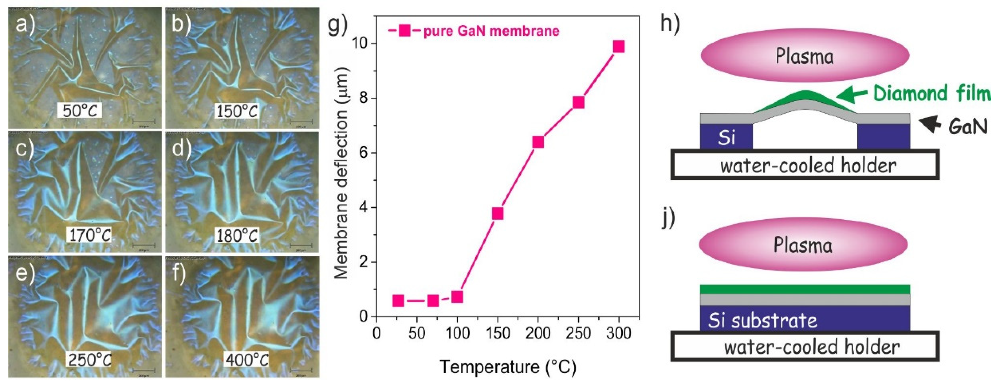
2. Methodology and Results

The diamond deposition on the GaN membranes with diameters of 1 mm was performed in an ellipsoidal cavity microwave plasma chemical vapor deposition (CVD) reactor [2]. After diamond deposition, the membrane area was not smooth, and many wrinkles were observed. This was primarily attributed to the different thermal expansion coefficient (TEC) of materials. When above 500 °C, the TECs of the diamond and GaN have nearly the same value (~4 ÷ 5 × 10⁻⁶ K−1), while at room temperature (RT), the TEC of GaN is 4 x higher than that of the diamond. The effect of membrane bulging can be illustrated by the reverse—heating up the diamond-coated GaN membrane from RT to the deposition temperature (Figure 1a–f). It was observed that the closer the temperature to the deposition temperature (~480 °C), the larger the bulging effect. However, wrinkles were still observed. For a better interpretation, we also measured the deflection of the pure GaN membrane by white light interferometry and the bulging method. It was observed that up to ~100 °C, the membrane deflection is minimal (~0.5 μm); however, above 100 °C, it nearly linearly increases with the temperature, and at 300 °C, its value reaches ~10 μm (Figure 1g).
Figure 1. (af) Optical photos of diamond-coated GaN membranes at different temperatures. (g) Deflection of the pure GaN membrane as a function of temperature. Schematic models of top-side diamond deposition on the GaN membrane (h) and solid GaN/Si substrate (j).
To conclude, the deposition of the diamond on GaN membranes at elevated temperature is technologically a complex issue, where induced stress is caused by abovementioned mismatch of TECs and the temperature gradient. However, we proposed an optimized technological procedure to obtain both-side diamond-coated GaN membranes with a minimized effect of wrinkling and induced residual stress.

Author Contributions

Conceptualization, T.I. and A.K.; methodology, T.I. and Š.P.; validation, G.V. and Š.P.; formal analysis, T.I.; investigation, T.I., M.D., M.V. and S.K.; resources, A.K. and J.Z.; writing—original draft preparation, T.I.; writing—review and editing, T.I., A.K., G.V., B.Z.; visualization, T.I.; supervision, A.K. and G.V.; project administration and funding acquisition, A.K., G.V., J.Z. and B.Z. All authors have read and agreed to the published version of the manuscript.

Funding

This research was funded by the Programme for Funding Multilateral Scientific and Technological Cooperation Projects in the Danube Region, grant No. DS-FR-19-0051 (8X20035), and by Operational Programme Research, Development and Education financed by European Structural and Investment Funds and Czech Ministry of Education, Youth and Sports (Project No. SOLID21-CZ.02.1.01/0.0/0.0/16_019/0000760). This work has used the large research infrastructure CzechNanolab supported by the Ministry of Education, Youth and Sports of the Czech Republic through the LM2018110 project, and was supported by grants of the Slovak Research and Development Agency, grant Nos. APVV-18-0243 and APVV-18-0273.

Conflicts of Interest

The authors declare no conflict of interest.

References

  1. Dzuba, J.; Vanko, G.; Vojs, M.; Rýger, I.; Ižák, T.; Jirásek, V.; Kutiš, V.; Lalinský, T. Finite element analysis of AlGaN/GaN micro-diaphragms with diamond coating. In Proceedings of the SPIE, Smart Sensors, Actuators, and MEMS VII; and Cyber Physical Systems, Barcelona, Spain, 4–6 May 2015; Volume 9517, p. 95171. [Google Scholar] [CrossRef]
  2. Izak, T.; Vanko, G.; Babchenko, O.; Potocký, Š.; Marton, M.; Vojs, M.; Choleva, P.; Kromka, A. Diamond-coated three-dimensional GaN micromembranes: Effect of nucleation and deposition techniques. Phys. Status Solidi B 2015, 252, 2585–2590. [Google Scholar] [CrossRef]
Publisher’s Note: MDPI stays neutral with regard to jurisdictional claims in published maps and institutional affiliations.

Article Metrics

Citations

Article Access Statistics

Multiple requests from the same IP address are counted as one view.