


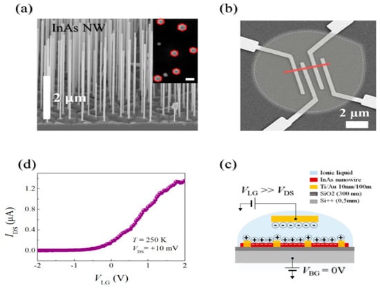
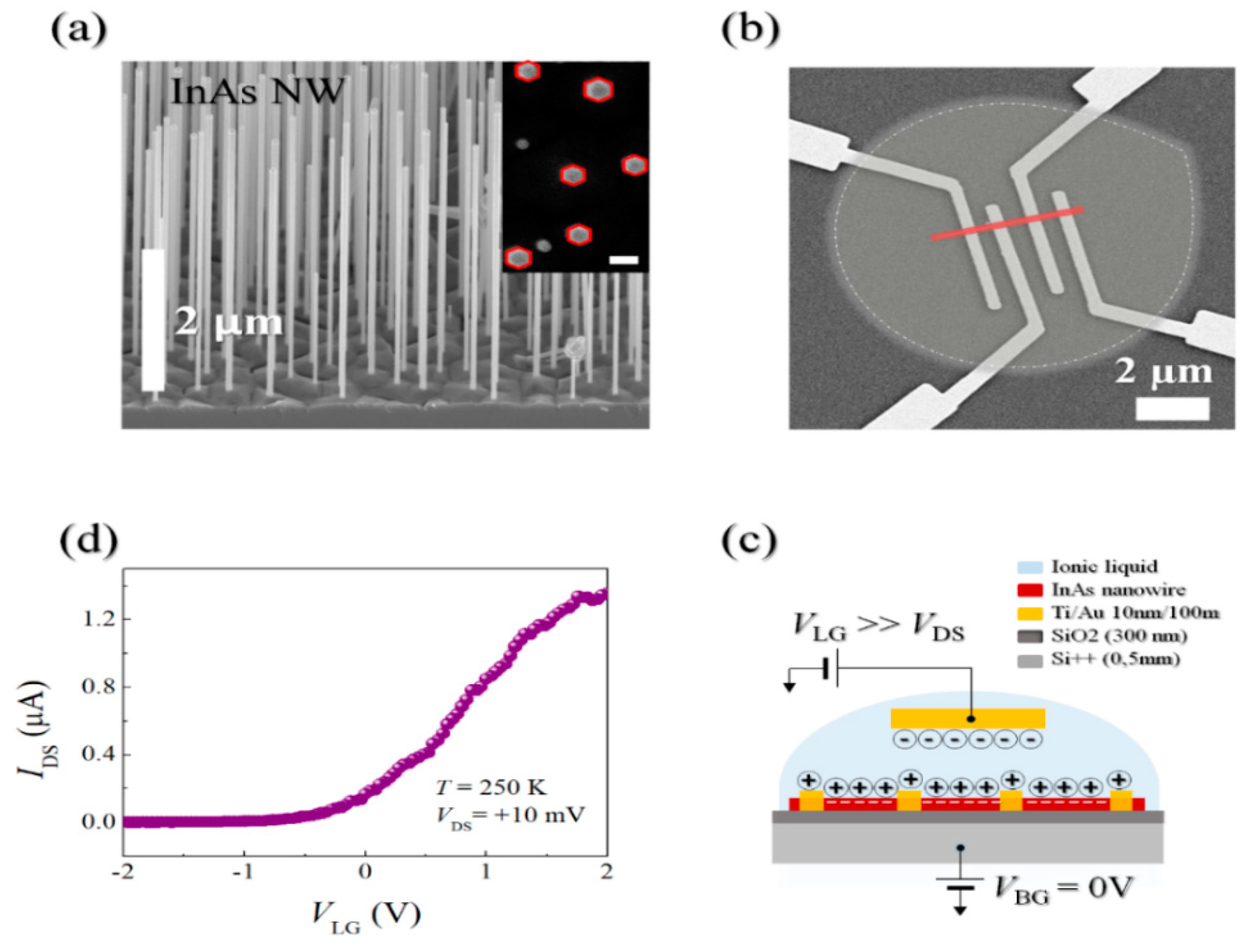
The operation of an ionic liquid-gated field effect transistor based on a single InAs nanowire—as represented in the SEM micrograph Figure 1b and pictorially in Figure 1c—is demonstrated. The voltage-biased ionic liquid implements the electric-double-layer inducing the field effect in the semiconductor nanostructure, and this allows to achieve the full control over the nanowire transistor (Figure 1d). The ionic liquid gate is up to 40 times more performing with respect to the back-gate. The temperature dependence of the resistance, measured for different doping levels, reveals a clear change in the behavior of the nanostructure from fully semiconducting to quasi-metallic. Perspectives of the use of liquid gating techniques to operate nanodevices based on III–V semiconductor nanostructures include fundamental and applied studies such as carrier density induced phase-transitions to bioelectronics, light emission and detection at the nanoscale, bio-sensing.
Figure 1.
(a) SEM micrograph (tilted view) of InAs nanowires grown by chemical beam epitaxy. Inset: Top view evidencing the hexagonal cross-section; (b) SEM micrograph (top view) of a prototypical InAs nanowire-FET: Four electrodes define three NW sections. The NW is red-colored; the ionic liquid drop is schematically depicted in overlay; (c) Schematic of a liquid electrolyte gated InAs nanowire FET; (d) Electrical current flowing in the NW as a function of the applied liquid gate voltage.
© 2018 by the authors. Licensee MDPI, Basel, Switzerland. This article is an open access article distributed under the terms and conditions of the Creative Commons Attribution (CC BY) license (https://creativecommons.org/licenses/by/4.0/).