1. Introduction
This paper gathers performance data of different types of single 2D material-based infrared (IR) and terahertz (THz) detectors. Their performance is compared with existing mature material systems including HgCdTe, InGaAs, III-V compounds and microbolometers. The intent is to concentrate on device architectures that can have the most impact on future position in wide high operating temperature (HOT) IR and THz detector family.
2. Graphene-Based Detectors
Graphene detectors can be divided into two categories: either photon and thermal (the bolometer effect) detectors. The majority of graphene pristine photodetectors exploit graphene metal junctions, graphene p-n junctions, and FET transistors.
The most recent approach also employs the photo-thermoelectric (PTE) effect (Seebeck effect) to create an electric field due to electron diffusion into metal contacts. The photocurrent direction due to both PV and PTE effects are the same.
The development of the graphene high responsivity photodetectors is determined by the two major challenges: the low optical absorption in the detector’s active region (~100–200 nm) and short photocarrier lifetime meaning that graphene photodetectors are mainly limited by trade-off between high responsivity, ultrafast time response and broadband operation.
Responsivity improvement in grapheme detectors can be reached by increasing the photocarrier lifetime through both band structure and defect engineering.
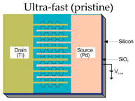
Table 1 shows schematically the differences between pure graphene photodetector and hybrid photodetector [
1]. Additionally, the distinction between ultrafast and ultrasensitive graphene photodetectors is presented.
The main feature of the hybrid photodetector is ultrahigh gain originating from the high carrier mobility of the graphene sheet and the recirculation of charge during the lifetime of the carriers remaining trapped in light absorbing region. Multiple circulation of holes in the graphene channel following a single e-h photogeneration leads to strong photoconductive gain.
Table 1.
Ultrafast and ultrasensitive graphene photodetectors.
Hybrid photodetectors offer improvements in responsivity, however the majority of these devices have a limited linear dynamic range due to the charge relaxation time, which quickly saturates the available states for photoexcitation, leading to a drop in responsivity with incident optical power.
3. Graphene-Based Detector Performance—The Present Status
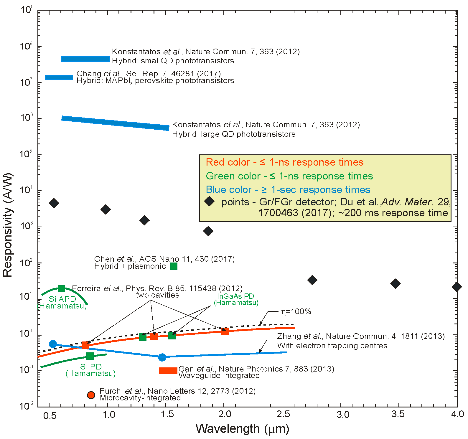
The spectral responsivity of graphene photodetectors operating in visible and NIR spectral ranges are compared with commercially available silicon and InGaAs photodiodes in
Figure 1. As shown, graphene’s high mobility together with the trapped charge lifetimes in the quantum dots produced a photodetector responsivity of 10
7 A/W. However, due to the long lifetime of the traps, the demonstrated frequency response is very slow (<10 Hz).
Literature data for longer wavelength infrared graphene-based photodetectors, with cut-off wavelength above 3 μm, are limited.
Figure 2 compares their detectivities with commercially available HgCdTe photodiodes and type-II InAs/GaSb superlattice interband quantum cascade infrared photodetectors (IB QCIPs) operating at room temperature. The upper detectivity of Gr/FGr photodetector in SWIR range is close to HgCdTe photodiodes. This figure also shows experimental data for black phosphorus arsenic (bAsP) photodetectors entering the second atmospheric transmission window. However, instability of the surface of bAsP, due to chemical degradation in ambient conditions, remains a major impediment to its prospective applications.
Particular attention in development of THz imaging systems is devoted to the fabrication of sensors with a large potential for real-time imaging while maintaining room temperature operation. Much of recent development is directed towards three types of focal plane arrays (FPAs): Schottky barrier diodes (SBDs) compatible with the CMOS process, FETs relying on plasmonic rectification effect, and adaptation of IR bolometers to the THz frequency range.
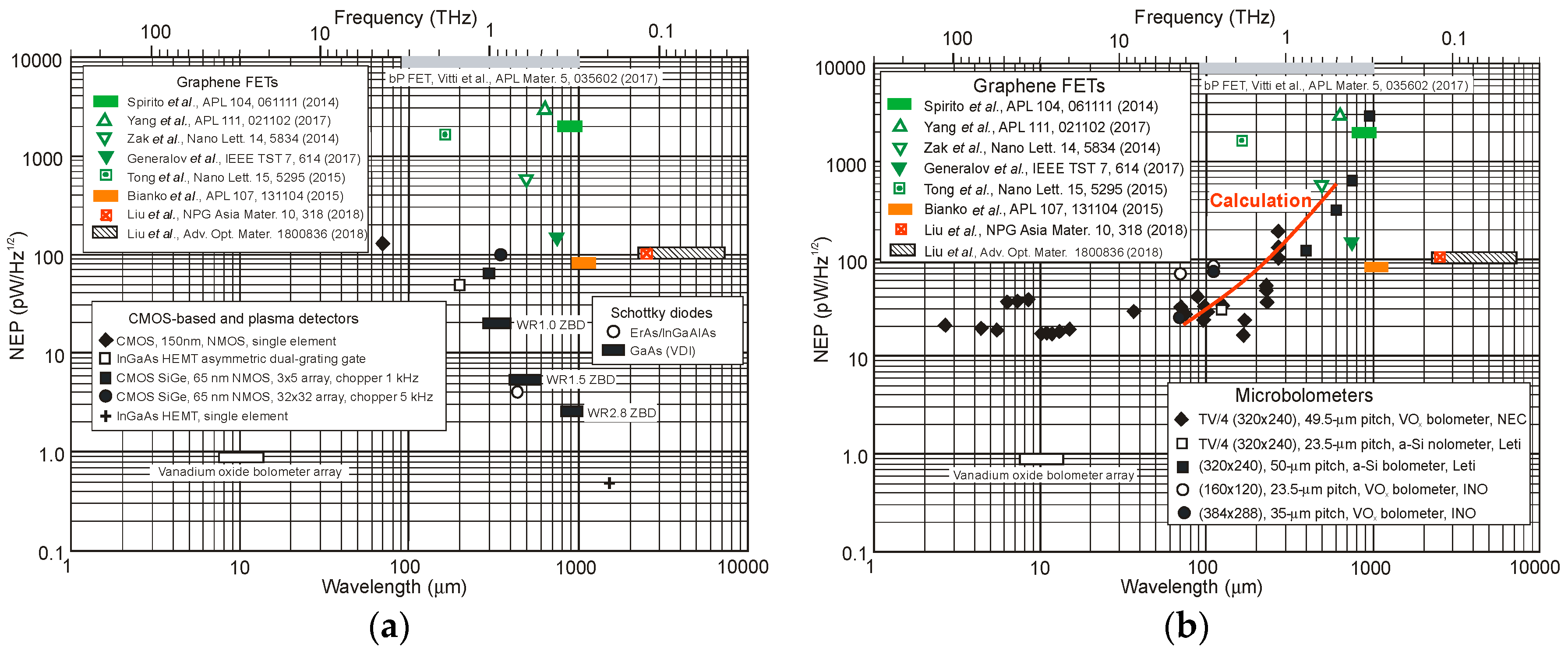
At present stage of technology, the most effective graphene THz detectors employ plasma rectification effect in FETs, where plasma wave in the channel are excited by incoming THz wave modulating the potential difference between gate and source/drain and being rectified via non-linear coupling and transfer characteristics in FET. Next two figures compare
NEP values of graphene-based FET room temperature detectors with existing THz photon detectors (
Figure 3a) and thermal detectors (
Figure 3b) dominating on the market. A lot of experimental data are gathered from world-wide literature.
Most experimental data gathered in literature is given for single graphene detectors operating above wavelength of 100 μm. Generally, the performance of graphene FET detectors is lower in comparison with CMOS based and plasma detectors fabricated using silicon, SiGe and InGaAs based materials. In comparison with VO
x and amorphous silicon microbolometers, the performance of graphene detectors is close to the trend line estimated for microbolometers in THz spectral region (see
Figure 3b). It should be marked here however, that microbolometer data are addressed to monolithic arrays. It appears, that the fabrication of monolithically integrated THz detector arrays encounters many technological problems that the device-to-device performance variations and even the percentage of non-functional detectors per chip tend to be unacceptably high.
4. Related Two-Dimensional Material Detectors
The discovery of new 2D materials with direct energy gaps in the infrared to the visible spectral regions has opened up a new window for photodetector fabrication. Even though the technology readiness levels are still low and device manufacturability and reproducibility remain a challenge, the 2D materials technology can be found in research labs around the globe including materials like silicene, germanene, stanene and phosphorene, transition metal dichalcogenides (TMDs), black phosphorus and recently discovered all inorganic perovskites.
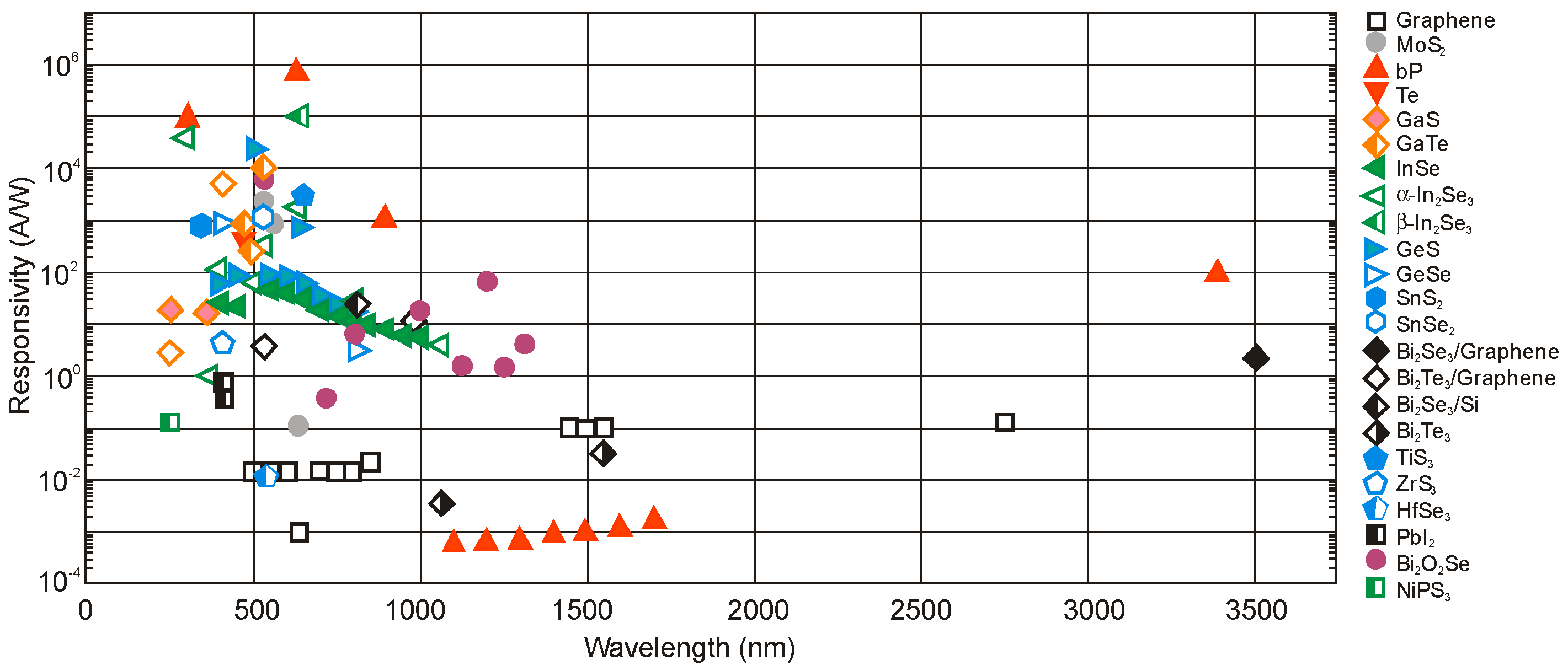
As is shown in
Figure 4, 2D layered materials show potential in photodetection covering UV, visible, IR and THz ranges. Generally however, most of them cover visible and near-IR (NIR) spectral range. At present stage of technology, only graphene-based, bPAs and bismuthene (like Bi
2Te
3 and Bi
2Se
3) play the role in IR and THz regions.
5. Conclusions
The performance of 2D material IR and THz detectors is lower in comparison with those detectors existing in global market, especially HgCdTe, InGaAs, type-II superlattice III-V compounds, and microbolometers. The most effective single graphene detectors operating at room temperature are THz detectors utilizing plasma rectification effect in FETs. Their performance is close to trend line estimated for microbolometer monolithic arrays in THz spectral region.
The discovery of alternative to graphene 2D materials with direct energy gaps has opened up a new window for photodetector fabrication. Most of layered semiconducting material photodetectors operate at the visible and near-infrared regions and generally their high sensitivity does not coincide with a fast response time. This indicates that 2D infrared photodetectors operated at room temperature are not ready for real applications.

