Proceeding Paper

Effect of Temperature and Electrical Modes on Radiation Sensitivity of MISFET Dose Sensors †

by
Boris Podlepetsky
*,
Viacheslav Pershenkov
,
Alexander Bakerenkov
,
Vladislav Felitsyn
and
Alexander Rodin
Micro- and Nanoelectronics Department, National Research Nuclear University MEPhI (Moscow Engineering Physics Institute), 115409 Moscow, Russia
*
Author to whom correspondence should be addressed.
Presented at the Eurosensors 2018 Conference, Graz, Austria, 9–12 September 2018.
Proceedings 2018, 2(13), 954; https://doi.org/10.3390/proceedings2130954
Published: 3 December 2018
(This article belongs to the Proceedings of EUROSENSORS 2018)

Abstract

:
The temperature and electrical modes influences on radiation sensitivity of n-channel MISFETs sensors of the total ionizing dose were investigated. There were measured the MISFET-based dosimeter output voltages V as function of the radiation doses D at const values of the drain current IDand the drain–source voltage VD, as well as the (IDVG) characteristics before, during and after irradiations at different temperatures T (VGis the gate voltage). It was shown how the conversion function V(D) and the radiation sensitivity SD are depending on the temperature T for different electrical modes. To interpret experimental data there were proposed the models taking into account the separate contributions of charges in the dielectric Qt and in SiO2–Si interface Qs. The model’s parameters ΔVt(D,T) and ΔVs(D,T) were calculated using the experimental IDVG characteristics. These models can be used to predict performances of MISFET-based devices.

1. Introduction

The influence of ionizing radiation (electrons, X-rays, γ-rays, protons and heavy ions) on devices based on the metal-insulator-semiconductor structures (MIS-capacitors and field-effect transistors called as MISFETs) are being studied since 1960’ years (e.g., [1,2]). It was found that the general dose radiation effect is the irreversible change during irradiation of effective charge Qe, summarized effective charges Qt in an insulator and Qs in insulator-semiconductor interface [3,4]. This effect results in the deformations of MIS-capacitors’ C-V characteristics and MISFETs’ IV characteristics (CVC), what are physical basics of the MIS-based dosimeters of ionizing radiation. MISFETs possess small sizes and the best compatibility with the elements of silicon integrated circuits (SIC). So as dose-sensitive elements they seem promising to develop the integrated dose-metric sensors, as well as embedded elements in SIC to estimate degradations of SICs’ electrical characteristics under irradiation. MISFET-based dosimeters are using in medicine and in space equipments.
MISFET-based sensors of the total ionizing dose D (TID) have been studied by many investigators [4,5,6,7,8]. Found that radiation sensitivity of sensors depend on electrical modes, structural and technological parameters of MISFET. We have previously researched n-channel MISFET as the dose-metric sensor at room temperature [8]. However, radiation changes of effective charges Qtand Qs at different temperatures T and electrical modes remain unexplored issues. The motivations of work are to investigate of the influence temperatures in wide ranges on the TID effects in MISFETs at different electrical modes, and to propose models taking into account the separate contributions of Qt(T,D) and Qs(T,D) to radiation sensitivity.
Usually, sensors embedded in signal conditioning analogue or digital circuits to measure TID. Typically, MISFETs applied in dosimeters in analogue modes. The informative parameter of the volt-metric analogue circuits is the output voltage V, which consists of the initial value V0 and dose-dependent value ΔV. The value ΔV is the result of converting the dose change ΔD in charge changes ΔQe. There are three basic electrical modes for volt-metric circuits: (1) the measurand V is VG vs. Qe at the constant ID and VD; (2) the measurand V is VD vs. ID(Qe) at the constant VG; (3) the measurand V is VD vs. Qe at the constant ID and VG. In this paper there will be analyzed only the first type of circuit used widely in MISFET-based devices.

2. Materials and Methods

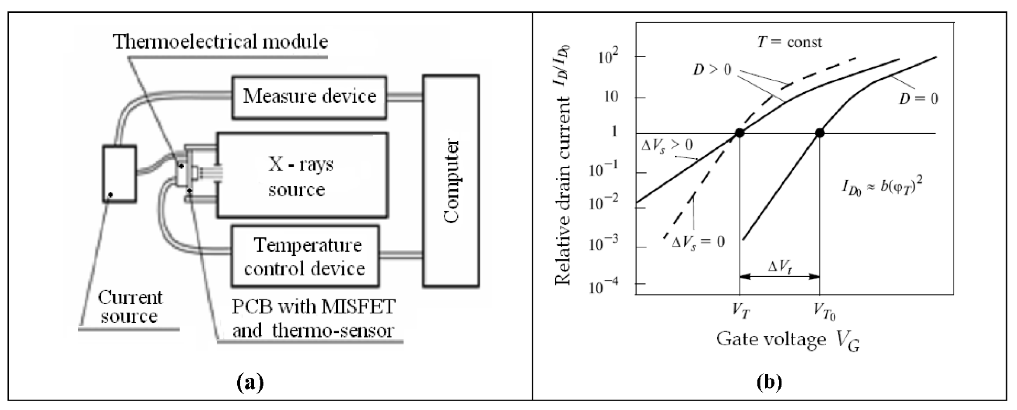
MISFETs with Al-SiO2-Si structure were fabricated by means of conventional n-MOS-technology. The chip and the circuit of MISFET-dosimeter demonstrated in Figure 1. In this circuitry the voltage V is equal to the gate voltage VG. The simplified structure of the all measuring system is shown in Figure 2a. There were measured the output voltages V as function of the total ionizing dose (TID) D of X-rays radiation for different drain currents IDand source-drain voltages VD, as well as the (IDVG) characteristics before, during and after irradiations at different temperatures T in range from −50 °C to 125 °C. The constant temperatures (T ± 2 °C) were supported by thermoelectrical module (Peltier element), using the temperature control circuitry of measuring system MERA-3. The general view of IV characteristics before and after irradiation at constant T is illustrated in Figure 2b.

3. Results

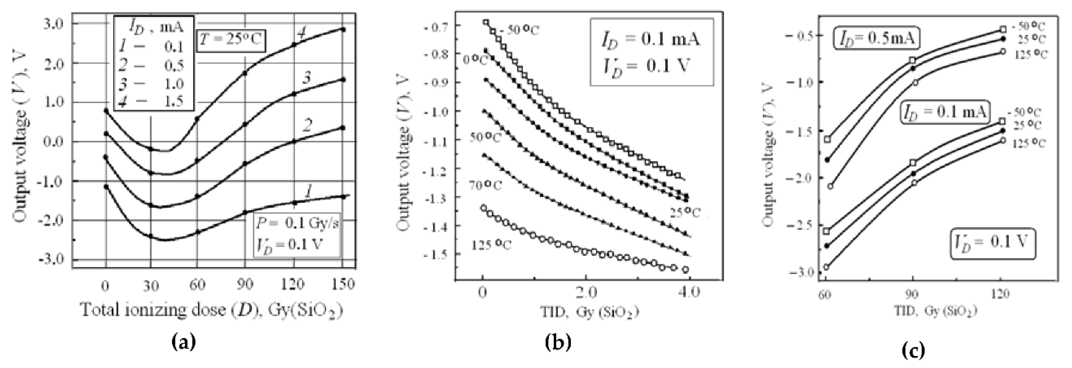
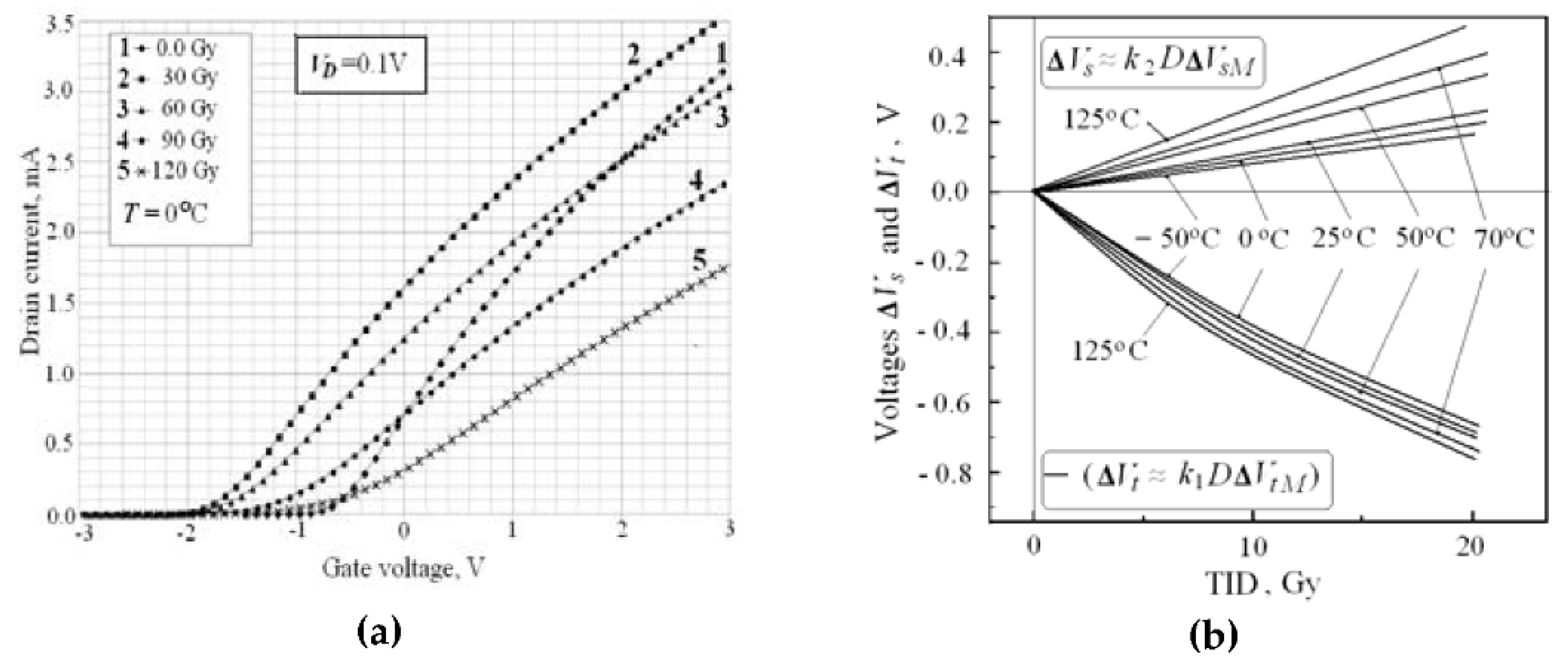
Experimental conversion functions V(D) at various currents ID and temperatures T are presented in Figure 3. The example of (IDVG) characteristics before and after irradiations is illustrated in Figure 4a. Calculated separate contributions of model’s parameters ΔVt(D,T) and ΔVs(D,T) at different temperatures and average values of parameters of MISFETs are presented in Figure 4b and in Table 1.

4. Discussion

The conversion functions V(D) have two areas (the negative and positive sensitivities). To interpret the results the following 3-component model of voltage V(D,T,ID)was used:
V(D,T,ID) = V0(T,ID) − ΔVt(D,T,ID) − ΔVs(D,T,ID),
ΔVt(D, T, ID) = ΔQt/C0 = ΔVtM[1 exp(−k1D)]; ΔVs (D,T) = ΔQs/C0 = ΔVsM[1 exp(−k2D)];
ΔVtM(T, ID) = (ΔQ0M +k0U)/C0]; at U = (VVT) > 0,
where V0 (T,ID) is an initial output voltage, being independent on TID, determined by experiments (see Table 1). Value C0 is the dielectric capacitance per unit area. Value V0 depends on temperature, electrical mode, structural and technological parameters of MISFET. The average temperature coefficient of initial output voltage α0 being equal to ΔV0/(V0ΔT) ×100 can be estimated as (−0.3%/K).Value VT is the threshold voltage of MISFET. The radiation sensitivity determined as
SD = dV/dD = k2ΔVsM∙exp(−k2D) − k1ΔVtM∙exp(−k1D).
If temperature increase, that maximum sensitivity SDM decreases for low TID and increase for high doses. The temperature coefficient of radiation sensitivity was estimated as αT = ΔSD/(SDΔT) × 100 being equal to 0.12%/K. The parameters of models (1)–(4) were calculated from the experimental IDVG characteristics as in [9].
To measure low doses (up to 10 Gy), it is recommended to use the initial conversion function areas in its linear region (the negative sensitivity area), where the maximum sensitivity slightly dependent on the electric mode. To measure doses over a wider range (up to 100 Gy), the conversion function areas with positive sensitivity can be used by pre-irradiating with a dose of ~50 Gy. In this case, the average radiation sensitivity is more dependent on the operating drain current and may even exceed the maximum sensitivity in the negative sensitivity area. However, the increase of operating current leads to increased power consumption and probability of “effect of self-heating”, when the temperature of the chip exceeds the temperature of the environment, and result in additional errors of doses’ measurement. For example, at VD = 0.1 V and the permissible power dissipation of 1 mW, the drain current should not exceed 10 mA, and the output voltage would be positive throughout the conversion range, the drain current should be greater than 1.5 mA. The drain current ID = 2.0 mA, corresponding to the average sensitivity S = 40 mV/Gy, can be considered optimal for the area of positive sensitivity of theMISFET-dosimeter.

5. Conclusions

The temperature influences on radiation sensitivity of n-channel MISFETs sensors of the total ionizing dose were investigated at different electrical modes. There were measured the MISFET-based dosimeter output voltages as function of TID at constant values of the drain currents, as well as the CVC before, during and after irradiations at different temperatures in range −50 °C to 125 °C. It was shown how the conversion function V(D) and the radiation sensitivity SD are depending on the temperature for different electrical modes. To interpret experimental data there were proposed the models taking into account the separate contributions of charges in the dielectric Qt and in SiO2–Si interface Qs. The model’s parameters of ΔVt(D,T) and ΔVs(D,T) were calculated using the experimental IDVG characteristics. These models can be used to predict performances of various types MISFET-based dosimeters.

Acknowledgments

Author acknowledges support from the MEPhI Academic Excellence Project (ContractNo.02.a03.21.0005).

Conflicts of Interest

The authors declare no conflict of interest.

References

  1. Collins, D.R.; Sah, C.T. Effects of X-rays on Characteristics of MOS Structures. Appl. Phys. Lett. 1966, 8, 124–128. [Google Scholar] [CrossRef]
  2. Mitchell, J.P. Radiation-Induced Space-ChargeBuildup in MOS Structures. IEEE Trans. Electron Devices 1967, 14, 764–774. [Google Scholar] [CrossRef]
  3. Ionizing Radiation Effects in MOS Devices and Circuits; Ma, T.P.; Dressendorfer, P.V. (Eds.) Willey & Sons: New York, NY, USA, 1989. [Google Scholar]
  4. Moreno, D.; Hughes, R.; Jenkins, M.; Drumm, C. A Simple Ionizing Radiation Spectrometer/Dosimeter Based on Radiation Sensing Field Effect Transistors (RadFETs); SAND97-0255C; Sandia National Laboratories: Albuquerque, NM, USA, 1997; pp. 26–28. [Google Scholar]
  5. Clifford, K.; Robinson, A.; Miller, D.; Davis, M. Overview of Sensors and Needs for Environmental Monitoring. Sensors 2005, 5, 4–37. [Google Scholar]
  6. Martinez-Garcia, M.S.; Simancas, F.; Palma, A.J.; Lallena, A.M.; Banqueri, J.; Carvajal, M.A. General purpose MOSFETs for the dosimetry of electron beams used in intra-operative radiotherapy. Sens. Actuators A 2014, 210, 175–181. [Google Scholar] [CrossRef]
  7. Pejovic, M.M. P-channel MOSFET as a sensor and dosimeter of ionizing radiation. Facta Univ. Ser. Electron. Energ. 2016, 29, 509–541. [Google Scholar] [CrossRef]
  8. Podlepetsky, B.I.; Sukhoroslova, Y.V. Influence of Electrical Modes on Sensitivity of MISFET Ionizing Radiation Dose Sensors. Procedia Eng. 2016, 168, 741–744. [Google Scholar] [CrossRef]
  9. Podlepetsky, B.I.; Bakerenkov, A.S.; Sukhoroslova, Y.V. Radiation sensitivity modeling technique of sensors’ MIS-transistor elements. Autom. Remote Control 2018, 79, 180–189. [Google Scholar] [CrossRef]
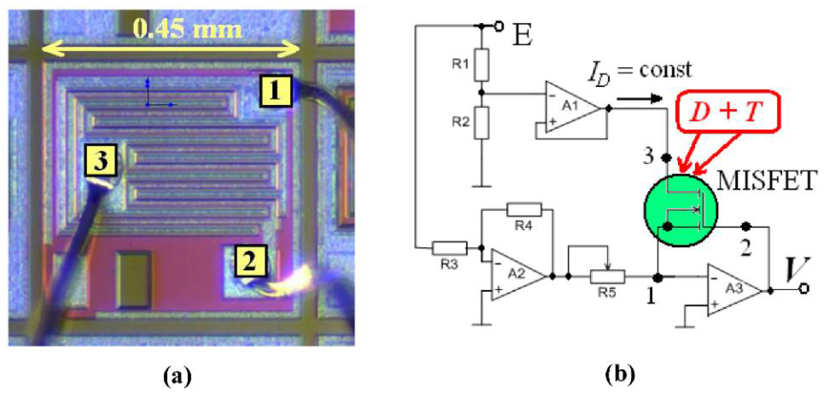
Figure 1. (a) MISFET’s chip photo; (b) The MISFET-dosimeter circuit (1—source; 2—gate; 3—drain).
Proceedings 02 00954 g001
Figure 2. (a) The structure of system MERA-3; (b) MISFETs’ IV characteristics before and after irradiation.
Proceedings 02 00954 g002
Figure 3. (a) Conversion functions at different ID; (b,c) Conversion functions at different temperatures T.
Proceedings 02 00954 g003
Figure 4. (a) ID–VG characteristics for different TID; (b) Calculated parameters ΔVt(D,T) and ΔVs(D,T).
Proceedings 02 00954 g004
Table 1. Average values (dispersion <10%) of parameters of MISFETs and models at ID = 0.1 mA.
T, °CV0,
V
ΔVtM,
V
ΔVsM,
V
k0,
nF/cm2
k1,
10−2Gy−1
k2,
10−2Gy−1
SDM1,
mV/Gy
SDM2,
mV/Gy
−50−0.672.593.8462.40.22−51.731.4
0−0.782.464.2422.50.26−51.031.6
25−0.872.464.4402.70.30−53.332.2
50−0.922.494.45402.80.40−53.133.5
70−1.122.514.6382.90.43−53.035.0
125−1.322.374.9353.10.51−48.537.2
Publisher’s Note: MDPI stays neutral with regard to jurisdictional claims in published maps and institutional affiliations.