Abstract
This study reports on a novel bi-stable actuator with an integrated aluminum nitride (AlN) piezoelectric layer sandwiched between two electrodes. To achieve bistability, the membranes must exceed a characteristic compressive stress value, also called the critical stress. For this purpose, we used highly c-axis orientated stress-controlled AlN with a thickness of 400 nm. First experiments showed, that it is possible to switch between the two stable ground states with at least two rectangular pulses at a frequency of 80 kHz and with a voltage Vpp of 40 V, resulting in a displacement of about 10 µm for each switching direction.
1. Introduction
Based on the growing market of mobile systems, the focus is nowadays on a low energy consumption of MEMS devices to ensure long operation times with limited power sources, such as batteries. Therefore, the power efficiency of MEMS sensors and actuators must be well optimized for future demands.
The bistability of membranes is regarded to be a promising feature to strongly decrease the power consumption of membrane-based MEMS devices due to the fact that energy is only needed when switching between the two ground states. Also, the displacement of bi-stable membranes is very high compared to standard configurations [1]. The bistability of membranes is well described in literature [2] showing two stable ground states. A membrane is bi-stable, when a characteristic compressive stress is applied, typically with an additional layer. Bi-stable systems are superior compared to conventional concepts when integrated in relays [3], non-volatile memory cells [4], energy harvesters [5] and valves [6]. In literature, the switching is typically done electrostatically [7,8], electromagnetically [6], thermally [9] or by exciting the device in resonance [10]. These concepts are either bulky, need very high voltage or current values or are restricted by the pull-in effect.
In this study we present a novel concept for switching between the ground states of a piezoelectric bi-stable membrane with an integrated sputter deposited aluminum nitride (AlN) layer which is piezoelectric and provides the necessary stress level. Furthermore, we show an electrical excitation concept to switch between the ground states by using short rectangular pulses.
2. Theory
Bistability at membranes occur when their intrinsic stress exceeds the characteristic value σc, also called the critical stress value. If this value is exceeded, the membrane has an initial deflection and two possible stable ground states (see Figure 1).
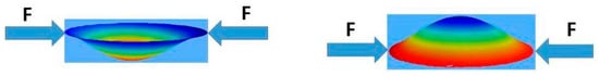
Figure 1.
The possible ground states of bistable membranes measured with a Whitelight interferometer.
This value can be calculated with the equilibrium of forces at the frame of a circular membrane when the bending moments are determined. By assuming pure plate behavior, the formula for the initial displacement w0 can be calculated [2]:
where σ0 is the initial stress, t the thickness, R the radius of the membrane, E the Young’s modulus and ν the passion’s ratio of the used material in the membrane. It is evident that the argument in the square root of Equation (1) must be larger than zero to get an initial deflection w0. This minimum stress value is called critical stress being for a circular membrane:
When a multilayer stack is used, the effective values of the material parameters and the intrinsic stress serve as approximation. For example the formula of the resulting stress of a N layer system is:
Basically, the effective values of the Young’s modulus and the Poisson’s ratio are calculated applying the same approach.
3. Fabrication
To simplify the fabrication process, the present approach uses silicon on isolator (SOI) wafers with a deposited 80 nm LPCVD stoichiometric silicon nitride on top of a 250 nm wet thermal oxide serving as insulation to the 2 µm thick device layer. To remove the oxinitride layer on the backside, the front side was protected with a spray-coated resist and the backside was etched with an oxygen plasma. The bottom electrodes were e-beam evaporated consisting of a bi-layer of 50 nm chrome and 200 nm gold and patterned with a lift-off process. Next, a negative photoresist was spray coated and developed for AlN structuring using again lift-off. The AlN layer was reactively sputter deposited with a VON ARDENNE LS730 sputter equipment at a chamber pressure of 2 µbar, a flow rate of 50 sccm nitrogen and a dc power of 800 W. Bow measurements at monitor wafers showed a compressive stress of the 400 nm thin AlN layer of σ0 = −600 MPa. The top electrode was e-beam evaporated and patterned in the same way as the bottom electrode. Wafer bow measurements showed a tensile stress of one electrode stack of σEl = +200 MPa. For DRIE etching of the backside with an OXFORD Instruments Plasmalab, the front side was protected with a thick spray coated photoresist. The buried oxide (BOX) with a thickness of 1 µm was used as etch stop and released with 40% buffered HF. After this process steps all of the membranes showed bi-stable behavior, indicated by buckling. Additionally, a wafer saw was used for dicing. The individual dies were cleaned with acetone to remove the protective resist on the device layer, isopropanol and distilled water, respectively. Finally, the membranes were bonded in a DIP-24 package for an easy connection to the electrodes. A schematic of the membranes in cross-sectional view is illustrated in Figure 2 on the left side, whereas the right side shows a bonded die with two membranes.
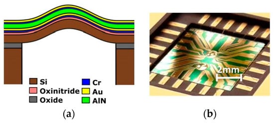
Figure 2.
(a) The conceptual design of the piezoelectric bistable membrane using a silicon membrane with AlN as piezoelectric layer sandwiched between top and bottom electrodes; (b) shows a bonded die with 2 membranes having multiple contacts to the electrodes.
4. Experimental Results
The movement of the membrane was measured with a set-up consisting of a Polytec MSA-400 as a laser Doppler Vibrometer (LDV), a HP Agilent 33124 function generator and a Trekstar 50× piezo amplifier which amplifies the signal of the function generator. The laser spot of the LDV was set to the center of the membrane and the MSA-electronics were triggered by the function generator. The measured velocity signal was then recorded and integrated over time in Matlab to obtain the displacement transient.
With the function generator, however, rectangular burst signals with two periods and with varying frequency can be applied which resulted in a switching between the two ground states. Figure 3 shows in the top graphs the applied voltage signal (blue) and the measured velocity characteristics during and after switching (red) and in the bottom graphs the calculated displacement of a 2.9 µm thick (i.e., 2 µm silicon device layer plus electrodes and 400 nm AlN) membrane with a diameter of 800 µm, whereas (a) illustrates the “switching down”, and (b) the “switching up” behavior. For this study two pulses of 40 Vpp and a frequency of 80 kHz were applied, which was not the resonance frequency of the membrane-based system.
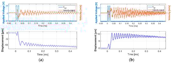
Figure 3.
In the top graphs the applied voltage (blue) und the measured velocity (red) are shown and in the bottom the calculated displacement of a 2.9 µm thick membrane with a diameter of 800 µm, whereas (a) shows the switching from the top ground state to the bottom ground state (e.g., “switching down”) and (b) the switching from the bottom to the top ground state (e.g., “switching up”).
It is worth mentioning that in this configuration it was not possible to switch the membrane with only one rectangular pulse. However, Figure 3 shows that it is possible to switch the ground states of a bi-stable membrane with an integrated AlN piezoelectric layer applying a minimum of two pulses. Displacements are in the range of 10 µm, which is hardly possible using AlN in a flat membrane configuration of these dimensions, featuring no bistability. The total displacement can be improved when the membrane is more compressively stressed (see Equation (1)), e.g., by using a thinner silicon device layer, a thinner stack of the tensile stressed electrodes or a thicker compressively stressed AlN film.
5. Conclusions and Outlook
This work presents the first bistable MEMS concept with an integrated piezoelectric thin film which can be very useful for some applications (e.g., pumps, switches). We showed that it is possible to switch between the stable states with rectangular pulses with 40 Vpp and measured a displacement of about 10 µm. The next step is to find an optimized electrode design and a signal characteristics for a low energy consumption bistable switching.
Acknowledgments
This project has been supported by the COMET K1 centre ASSIC Austrian Smart Systems Integration Research Center. The COMET—Competence Centers for Excellent Technologies-Programme is supported by BMVIT, BMWFW and the federal provinces of Carinthia and Styria.
References
- Wang, D.-A.; Pham, H.-T.; Hsieh, Y.-H. Dynamical switching of an electromagnetically driven compliant bistable mechanism. Sens. Actuators Phys. 2009, 149, 143–151. [Google Scholar] [CrossRef]
- Schomburg, W.K.; Goll, C. Design optimization of bistable microdiaphragm valves. Sens. Actuators A Phys. 1998, 64, 259–264. [Google Scholar] [CrossRef]
- Qiu, J.; Lang, J.H.; Slocum, A.H. A curved-beam bistable mechanism. J. Microelectromech. Syst. 2004, 13, 137–146. [Google Scholar] [CrossRef]
- Halg, B. On a micro-electro-mechanical nonvolatile memory cell. IEEE Trans. Electron. Devices 1990, 37, 2230–2236. [Google Scholar] [CrossRef]
- Andò, B.; Baglio, S.; Bulsara, A.R.; Marletta, V.; Medico, I.; Medico, S. A double piezo—Snap through buckling device for energy harvesting. In Proceedings of the 2013 Transducers & Eurosensors XXVII: The 17th International Conference on Solid-State Sensors, Actuators and Microsystems (TRANSDUCERS & EUROSENSORS XXVII), Barcelona, Spain, 16–20 June 2013; pp. 43–45. [Google Scholar]
- Uusitalo, J.-P.; Ahola, V.; Soederlund, L.; Linjama, M.; Juhola, M.; Kettunen, L. Novel Bistable Hammer Valve For Digital Hydraulics. Int. J. Fluid Power 2010, 11, 35–44. [Google Scholar] [CrossRef]
- Krylov, S.; Ilic, B.R.; Schreiber, D.; Seretensky, S.; Craighead, H. The pull-in behavior of electrostatically actuated bistable microstructures. J. Micromech. Microeng. 2008, 18, 055026. [Google Scholar] [CrossRef]
- Krylov, S.; Ilic, B.R.; Lulinsky, S. Bistability of curved microbeams actuated by fringing electrostatic fields. Nonlinear Dyn. 2011, 66, 403. [Google Scholar] [CrossRef]
- Qiu, J.; Lang, J.H.; Slocum, A.H.; Weber, A.C. A bulk-micromachined bistable relay with U-shaped thermal actuators. J. Microelectromech. Syst. 2005, 14, 1099–1109. [Google Scholar] [CrossRef]
- Casals-Terre, J.; Fargas-Marques, A.; Shkel, A.M. Snap-Action Bistable Micromechanisms Actuated by Nonlinear Resonance. J. Microelectromech. Syst. 2008, 17, 1082–1093. [Google Scholar] [CrossRef]
Publisher’s Note: MDPI stays neutral with regard to jurisdictional claims in published maps and institutional affiliations. |
© 2019 by the authors. Licensee MDPI, Basel, Switzerland. This article is an open access article distributed under the terms and conditions of the Creative Commons Attribution (CC BY) license (https://creativecommons.org/licenses/by/4.0/).