Abstract
Arrays of 1D-vertically arranged gallium nitride (GaN) nanorods (NRs) are fabricated on sapphire and connected to both bottom and freestanding top contacts. This shows a fully validated top-down method to obtain ordered arrays of high-surface-to-volume elements that can be electrically interrogated and used, e.g., for sensing applications. Specifically, these will be used as highly integrated heating elements for conductometric gas sensors in self-heating operation. Detailed fabrication and processing steps involving inductively coupled plasma reactive ion etching (ICP-RIE), KOH-etching, interspace filling, and electron-beam physical vapor deposition technologies are discussed, in which they can be well adjusted and combined to obtain vertical GaN NRs as thin as 300 nm in arbitrarily large and regular arrays (e.g., 1 × 1, 3 × 3, 9 × 10 elements). These developed devices are proposed as a novel sensor platform for temperature-activated measurements that can be produced at a large scale offering low-power, and very stable temperature control.
1. Introduction
It has been demonstrated that 1D-nanorods, offer very large surface-to-volume ratio, high chemical- and thermal-stability, and dimensions comparable to the extension of surface charge region, which make them potential candidates for the development and production of simple, power-efficient, reliable, cost-effective, and sensitive gas sensors [1]. GaN nanorods in combination with surface coatings can lead to the sensor resistance changes under exposure to gases, even at very low concentration [2]. Previous works in the production of NRs for sensing purposes were mostly focused on other more conventional materials, like metal-oxides or carbon-nanostructures, and mostly with lateral orientation [3,4,5,6]. Here, we choose to investigate the integration of GaN NRs in a vertical architecture following a fully top-down approach. This facilitates fabrication processing at a large scale, leads to better reproducibility, and allows for a good exchange of gases with the atmosphere. Also, the 1D- shape of the NRs and their ordered operation serve as clear parallel electron transfer pathway, which can be operated, e.g., as a Joule self-heating platform (Figure 1), with low power requirements, fast thermal response, and stable operation. [1,3,4].
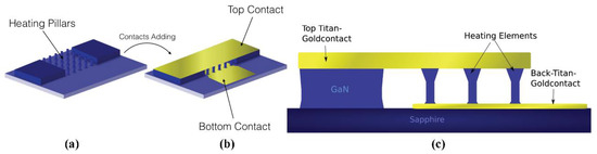
Figure 1.
Illustration of the device design: (a) before and (b) after contact creation. (c) Cross-sectional view of a finished heating platform.
2. Device Fabrication
Vertically arranged and contacted GaN-nanorod arrays were fabricated, starting with a bulk GaN layer on a sapphire wafer via top-down processing using photolithography, two-step ICP-RIE at room temperature, and two-step KOH-etching at 85 °C. The employed etching method is an enhancement of single-step GaN hybrid etching that has been implemented for creating vertical nanoelectronics (e.g., field-effect transistors [7,8,9]).
The so-called two-step hybrid etching method combining SF6/H2-based ICP-RIE and wet KOH etching is necessary for etching the GaN NRs completely down to the sapphire (Figure 2a–f. This step is critical as the isolation of every single NR must be guaranteed, so that the GaN bulk or the GaN buffer region will not contribute to the required power for driving the NR elements. Additionally, the currents that pass through the rods can be well controlled by adjusting their dimension and number. This etching step for insulating purpose is not straightforward especially for 3D GaN nanostructures with very high aspect ratios. In this case the total height of the rods that needs to be etched is around 4.4 μm.
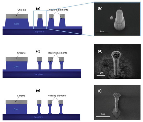
Figure 2.
Process steps for the two-step ICP-RIE and two-step KOH etching. Schematics and SEM images of nanorod array after (a,b) the first ICP-RIE, (c,d) the first KOH etching for smoothing NR surface and reducing its diameter size, and (e,f) the subsequent second ICP-RIE and the second KOH etching for the final surface smoothing treatment.
General GaN thinning methods including the single-step hybrid etching technique [7,8] may result in a fragile structure, regardless of the obtained 300 nm rod diameter. Therefore, the intermediate thinning (i.e., shrinkage of the rod only at its middle part) as proposed in this work offers a beneficial way for realizing more stable NR arrays with solid pedestal against any mechanical harm. Besides, for the following processing step, the bottom contact can have an improved attachment to the NR.
After the GaN NR arrays have been patterned, the bottom contact was produced by means of evaporation of metal thin layers with EBPVD. Meanwhile, the free-standing top contact fabrication required adequate filling of the spaces between the NRs, prior to metallization. This filling was a sacrificial layer consisting of AZ5214E Photoresin. Finally, the sacrificial filler was removed, leading to fully exposed NRs (Figure 1c).
From the used mask designs, the arrays could be fabricated either as a single NR or arrays of 9 NRs (3 × 3 array) and 90 NRs (9 × 10) with different NR diameters from 1.4 μm down to 1.0 μm. These initial diameters could be further thinned down to 300 nm after the second KOH-etching process.
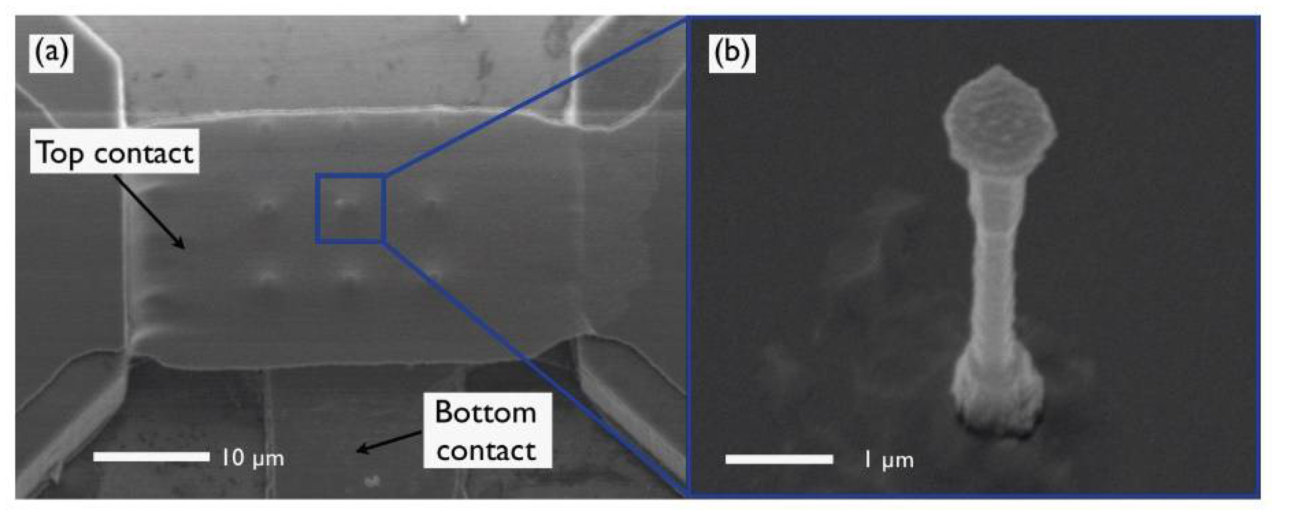
Figure 3a,b show a SEM image of (a) a top and bottom contacted GaN NR array and (b) a single non-contacted GaN NR. Further tests indicated that low power values (in the range of several hundred μW) are sufficient to heat up an array of 90 NRs to 200 °C, which means that around a few μW is required for a single NR. In terms of efficiency, this has led to specific Efficient Self-Heating (ESH) values [1] in the order of 10–100 K/μW, which is comparable with the best results achieved so far in literature but with a much easier fabrication process (instead of e.g., FIB-lithography and nanomanipulation) [1,2,3,4,5,6].
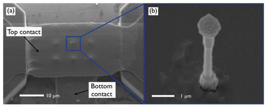
Figure 3.
(a) Array of 3 × 3 nanorods with top and bottom connection. (b) Single GaN nanorod with 300 nm diameter with intermediate narrowing.
3. Conclusions
Arrays of 1D-vertically arranged gallium nitride (GaN) nanorods (NRs) were fabricated on sapphire and connected to both bottom and freestanding top contacts. Detailed fabrication and processing steps were discussed including the two-step ICP-RIE at room temperature, and two-step KOH-etching, resulting in fully working Self-Heating Platforms. These developed devices are proposed as a novel sensor platform for temperature-activated measurements that can be produced at a large scale offering low-power, and very stable temperature control.
Author Contributions
N.M., M.F.F., O.C., H.S.W., A.W., and J.D.P. designed the concept of vertical GaN nanowire sensing platform. N.M. and A.G. developed the device processing steps and performed the experiments; M.F.F. designed the device mask; N.M. and K.S. performed optical characterization; N.M., O.G., H.S.W., and J.D.P. analyzed the experimental results; N.M. wrote the paper; N.M., H.S.W., A.W., and J.D.P. revised the paper and provided significant inputs on writing; H.S.W., A.W., and J.D.P led the development of the GaN device platforms at TU Braunschweig and University of Barcelona.
Acknowledgments
This work has been partially performed within EU Project of “BetterSense - Nanodevice Engineering for Better Chemical Gas Sensing Technology” funded by European Research Council under grant agreement no. 336917 and LENA-OptoSense funded by the Lower Saxony Ministry for Science and Culture (N-MWK). The authors thank A. Schmidt, J. Breitfelder, and M. Rühmann for their technical support during the experiments in clean room. K.S., H.S.W, and A.W. acknowledge support from the German Research Foundation (DFG) within “3D Concepts for Gallium-Nitride Electronics (3D GaN)” project.
Conflicts of Interest
The authors declare no conflict of interest.
References
- Fabrega, C.; Casals, O.; Hernandez-Ramirez, F.; Prades, J.D. A review on efficient self heating in nanowire sensors: Prospects for very-low power devices. Sens. Actuators B 2018, 256, 797–811. [Google Scholar] [CrossRef]
- Wagner, A.; Bakin, A.; Otto, T.; Zimmermann, M.; Jahn, B.; Waag, A. Fabrication and Characterization of Nanoporous ZnO Layers for Sensing Applications. Thin Solid Films 2012, 14, 4662–4665. [Google Scholar] [CrossRef]
- Chikkadi, K.; Muoth, M.; Maiwald, V.; Roman, C.; Hierold, C. Ultra-low power operation of self-heated, suspended carbon nanotube gas sensors. Appl. Phys. Lett. 2013, 103, 223109. [Google Scholar] [CrossRef]
- Prades, J.D.; Jimenez-Diaz, R.; Hernandez-Ramirez, F.; Barth, S.; Cirera, A.; Romano-Rodriguez, A.; Mathur, S.; Morante, J.R. Ultralow power consumption gas sensors based on self-heated individual nanowires. Appl. Phys. Lett. 2008, 93, 123110. [Google Scholar] [CrossRef]
- Ramgir, N.; Datta, N.; Kaur, M.; Kailasaganapathi, S.; Debnath, A.K.; Aswal, D.K.; Gupta, S.K. Metal Oxide Nanowires for Chemiresistive Gas Sensors: Issues, Challenges a Prospects Colloids Surface A Physicochem. Eng. Asp. 2013, 439, 101–116. [Google Scholar] [CrossRef]
- Afshar, M.; Preiss, E.M.; Sauerwald, T.; Rodner, M.; Feili, D.; Straub, M.; König, K.; Schütze, A.; Seidel, H. Indium-tin-oxide single-nanowire gas sensor fabricated via laser writing and subsequent etching, Sens. Actuators B Chem. 2015, 215, 525–535. [Google Scholar] [CrossRef]
- Yu, F.; Yao, S.; Römer, F.; Witzigmann, B.; Schimpke, T.; Strassburg, M.; Bakin, A.; Schumacher, H.W.; Peiner, E.; Wasisto, H.S.; et al. GaN nanowire arrays with nonpolar sidewalls for vertically integrated field-effect transistors. Nanotechnology 2017, 28, 95206. [Google Scholar] [CrossRef] [PubMed]
- Yu, F.; Strempel, K.; Fatahilah, M.F.; Zhou, H.; Römer, F.; Bakin, A.; Witzigmann, B.; Schumacher, H.W.; Wasisto, H.S.; Waag, A. Normally Off Vertical 3-D GaN Nanowire MOSFETs with Inverted—GaN Channel. IEEE Trans. Electron Devices 2018, 65, 2439–2445. [Google Scholar] [CrossRef]
- Yu, F.; Rümmler, D.; Hartmann, J.; Caccamo, L.; Schimpke, T.; Strassburg, M.; Gad, A.; Bakin, A.; Wehmann, H.-H.; Witzigmann, B.; et al. Vertical architecture for enhancement mode power transistor based on GaN nanowires. Appl. Phys. Lett. 2016, 108, 213503. [Google Scholar] [CrossRef]

Publisher’s Note: MDPI stays neutral with regard to jurisdictional claims in published maps and institutional affiliations. |
© 2018 by the authors. Licensee MDPI, Basel, Switzerland. This article is an open access article distributed under the terms and conditions of the Creative Commons Attribution (CC BY) license (https://creativecommons.org/licenses/by/4.0/).