1. Introduction
ZnO is a wide direct band gap semiconductor with attractive optoelectronic and piezoelectric properties, making it particularly appealing for a variety of sensors and actuators. ZnO thin films have been applied to gas [
1,
2], bio [
3], and UV sensors [
4] as well as piezoelectric nanogenerators [
5] and actuators [
6]. Tuning the optical and structural properties of ZnO coupled with precise thin film thickness control is crucial for enhancing the devices’ efficiency and sensitivity [
7,
8].
Among the techniques adopted to deposit ZnO thin films, atomic layer deposition (ALD) has become the method of choice for the growth of high-quality conformal films with Å-level thickness control [
9]. In ALD, thin film deposition occurs from the vapor phase. The substrate is sequentially exposed to two precursors, separated by an inert gas purge, defining one deposition cycle. Chemisorption of the precursors on the active groups present solely on the substrate surface ensures the self-limiting nature of the reactions and offers the possibility to control the film thickness by adjusting the number of cycles rather than the process time as in conventional chemical vapor deposition (CVD) processes. A typical growth per cycle (GPC) for ALD is in the Å/cycle range [
10]. In conventional ALD, the surface reactions are driven by thermal energy generally provided by substrate heating. In order to deposit high quality materials at lower temperatures, plasma-enhanced atomic layer deposition (PE-ALD) is often adopted [
11]. Here, reactive plasma species are used as co-reactants, ensuring self-limiting surface reactions also at room temperature.
In a recent study, polycrystalline ZnO thin films were deposited by PE-ALD at room-temperature by using diethylzinc (DEZ) and O
2-plasma as the reactant and oxidizing co-reactant, respectively [
12]. X-ray diffraction (XRD) revealed a (100) texture of the films in specular direction and the high quality of the films was confirmed by X-ray photoelectron spectroscopy which showed a carbon content of ~1% and a Zn/O-ratio ~1. Important properties of the films were easily tuned by modifying the radio frequency (RF)-power during the plasma exposure step such as the refractive index (1.81 to 1.88 at 633 nm), crystallite size (from 20 to 26 nm), and bandgap (from 3.22 to 3.27 eV) while the growth behavior stayed constant.
However, the applied RF-power showed a limited influence on the texture of the polycrystalline films. In the literature, it is reported that the substrate temperature has a strong effect on the texture. Park et al. [
13] showed that ZnO films prepared at 75 °C showed rather (100) preferred orientation whereas films prepared at 150 °C showed rather (002) preferential orientation. Zhang et al. [
14] compared films prepared with PE-ALD and thermal ALD and report a preferential (002) orientation for PE-ALD adopting substrates of 150 °C and above. Starting from the investigations of PE-ALD of ZnO at room temperature [
12], in this contribution the authors aim at exploring the texture of the films in a wider temperature range from 50–200 °C.
2. Materials and Methods
ZnO thin films were grown by plasma-enhanced atomic layer deposition in a custom-built direct plasma reactor. Single side polished silicon (100) wafers with a native oxide layer were used as substrates (Siegert Wafer). A strip heater (CSH00225, Omega Engineering, 75392 Deckenpfronn, Germany) was used to heat the substrates during deposition and the substrate temperature was varied between 50 °C and 200 °C. Diethlyzinc (optoelectronic grade, Dockweiler Chemicals, 35041 Marburg, Germany) and pure O2-plasma were used as metalorganic precursor and oxidizing co-reactant, respectively. Ar was used as the purging gas. The vacuum system consisted of a turbomolecular and a rotary vane pump. The working pressure was controlled using a butterfly valve and kept at around 75 mTorr during plasma exposure.
The ALD recipe consisted of four steps: (1) DEZ dose, (2) Ar purge, (3) O
2-plasma dose (with a 10 s oxygen flow stabilization prior to plasma ignition), and (4) Ar purge. Spectroscopic ellipsometry (M-2000V, J. A. Woollam Co., Lincoln, NE 68508, USA) was performed to determine the thickness and optical constants of the films. The spectra were measured at 65°, 70°, and 75° in a wavelength range of 370 to 1000 nm, and modeled in the ZnO transparent region (450–1000 nm) with a Cauchy model. Grazing incidence X-ray diffraction (GIXD) was performed at the XRD1-beamline at Elettra, Trieste. The wavelength for the primary beam was set at 1.4 Å, under an incident angle α of 0.5° and the diffracted intensities were collected on a Pilatus 2M detector. All data have been recalculated to (wavelength-independent) reciprocal space maps using the software package GidVis (
https://www.if.tugraz.at/amd/GIDVis/). Intensities are plotted in a pseudo-color representation as a function of the specular (q
z) and the in-plane component (q
xy) of the scattering vector.
3. Results and Discussion
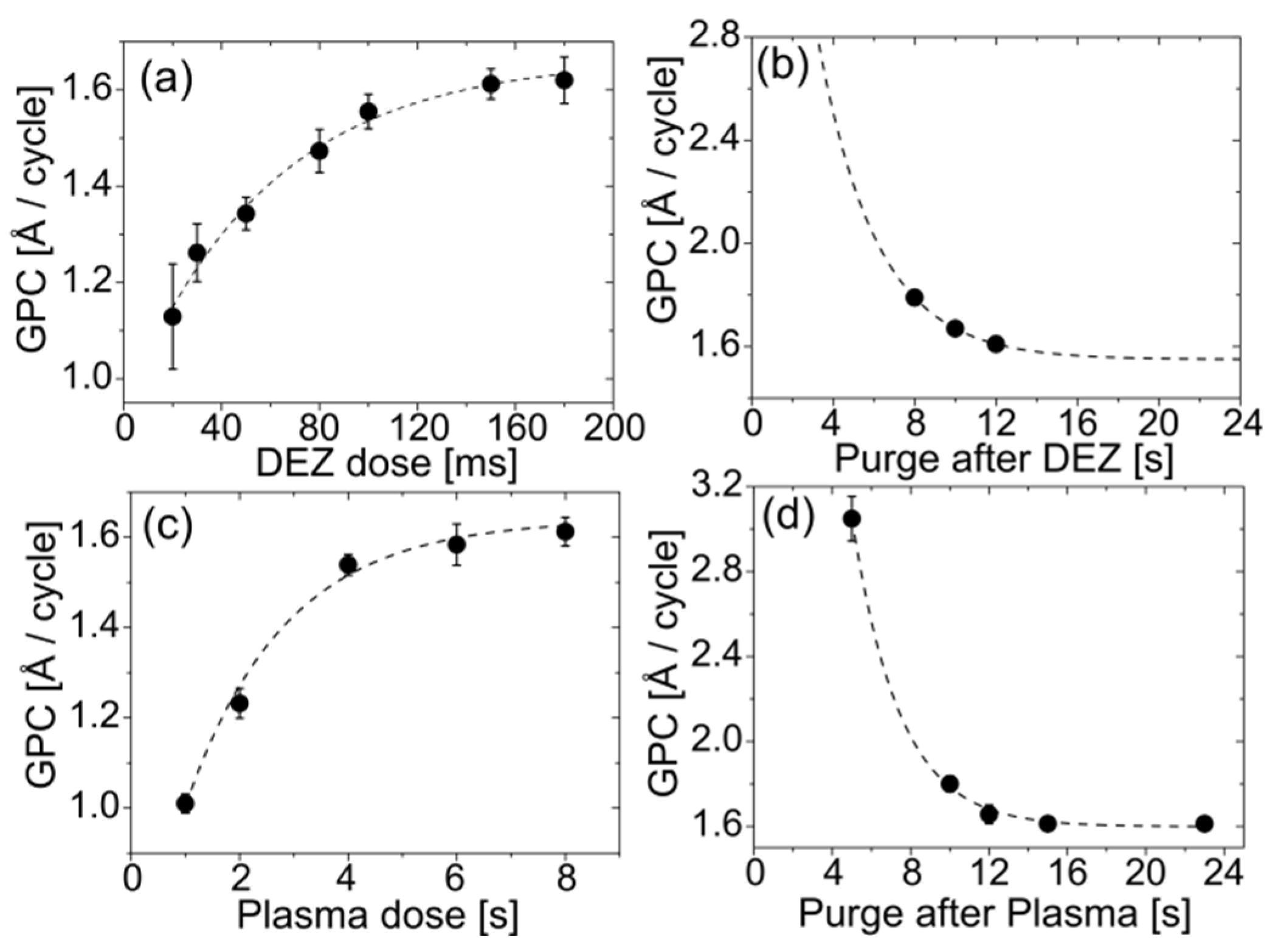
Figure 1 shows the saturation behavior of the four steps. The growth per cycle saturated at 1.6 Å/cycle and ALD growth was found adopting the following recipe: 0.15 s/12 s/8 s/15 s (DEZ dose/Ar purge/O
2-plasma dose/Ar purge).
The self-limiting nature of ALD-growth and the cyclic control of the thickness relies on saturated reactant and purging steps. The surface has to be exposed to enough precursor molecules to react with all available sites on the surface. Subsequently, the O2 plasma step should be sufficient to remove all organic ligands, leaving active surface sites for the next cycle. Furthermore, the purging steps have to be long enough to remove all unreacted precursor molecules and by-products, which would otherwise react in the vapor-phase with the subsequent precursor, and contributing to the growth with an uncontrolled CVD-like component.
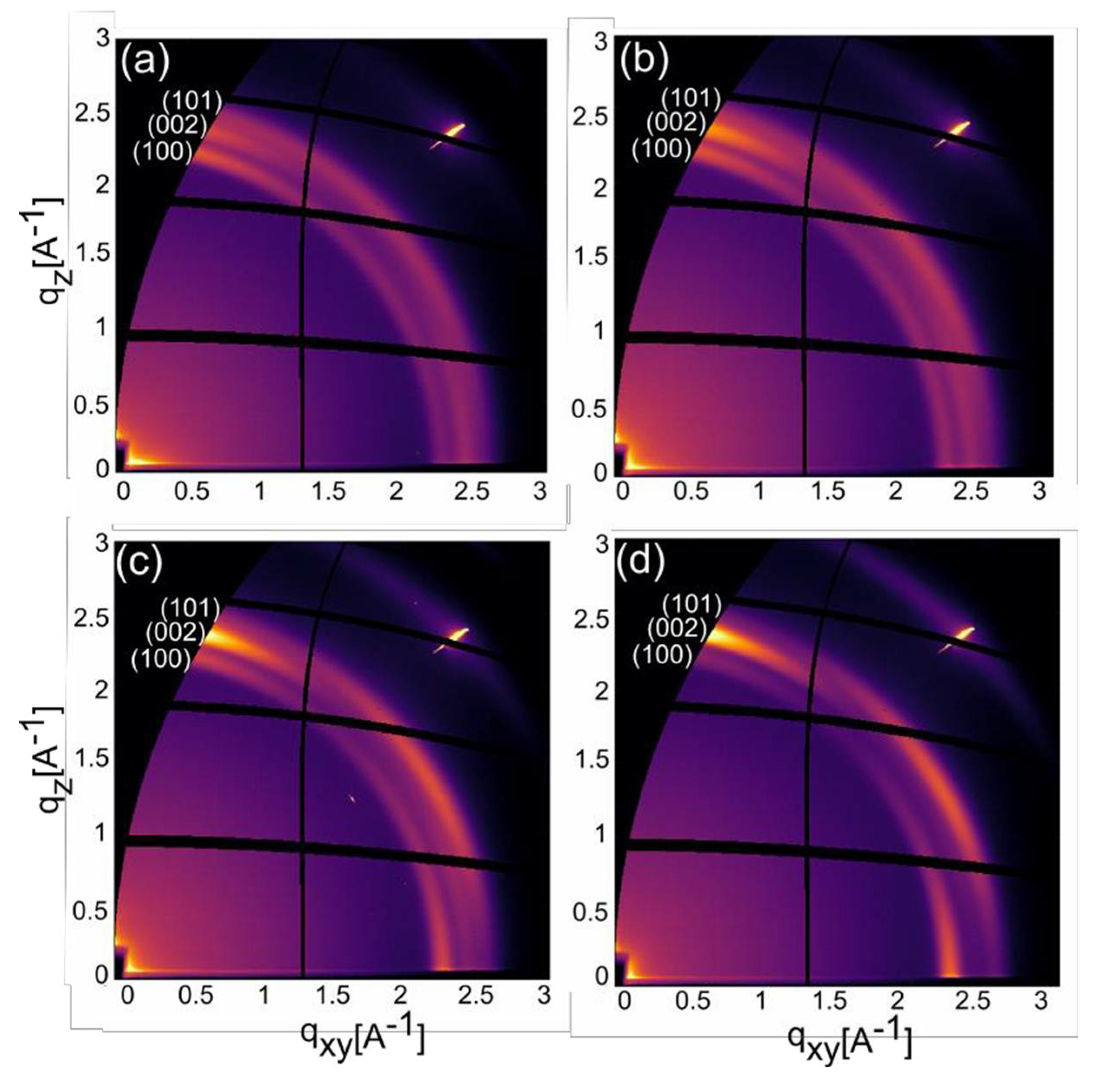
Adopting the optimized recipe, 30-nm-thick films were deposited at different substrate temperatures and analyzed by GIXD to obtain in-plane and out-of-plane structural information. The GIXD-maps are reported in
Figure 2. Temperature was found to strongly affect the texture of the films, in line with the literature [
13,
14]. By increasing the temperature, the intensity of the (002) peak increases towards the out-of-plane direction (q
z) and becomes more pronounced. By tuning the substrate temperature, it is thus possible to obtain rather (100) textured films at low temperatures or (002) textured films at higher temperatures.
Switching of the film’s texture of the films could be an important feature in applications such as piezoelectric devices [
15] or photocatalysis [
16]. In fact, it was shown that texture is among the most important properties for enhancing device related features such as piezo-responsiveness or photocatalytic performance.
In conclusion, PE-ALD was adopted for the deposition of high quality ZnO thin films. By varying two parameters in the deposition process, i.e., the plasma RF-power [
12] and the substrate temperature, the most important material parameters of the ZnO thin films such as refractive index, bandgap, and crystallite size [
12] as well as the texture can be tuned. Further investigations will focus on the conductivity, piezoresponse, and transparency of the ZnO thin films.
Author Contributions
J.P. performed the experiments (not including GIXD measurements), analyzed the data, and wrote the paper, A.P. and A.M.C. conceived and designed the experiments, and A.M.C. supervised the project.
Acknowledgments
This project has received funding from the European Research Council (ERC) under the European Union’s Horizon 2020 research and innovation program (Grant Agreement No. 715403). The authors thank Sebastian Hofer and Andreas Hofer for performing the GIXD measurements.
Conflicts of Interest
The authors declare no conflict of interest. The founding sponsors had no role in the design of the study; in the collection, analyses, or interpretation of data; in the writing of the manuscript, and in the decision to publish the results.
References
- Sahay, P.P. Zinc oxide thin film gas sensor for detection of acetone. J. Mater. Sci. 2005, 40, 4383–4385. [Google Scholar] [CrossRef]
- Zhu, L.; Zeng, W. Room-temperature gas sensing of ZnO-based gas sensor: A review. Sens. Actuators A Phys. 2017, 267, 242–261. [Google Scholar] [CrossRef]
- Singh, S.P.; Arya, S.K.; Pandey, P.; Malhotra, B.D.; Saha, S.; Sreenivas, K.; Gupta, V. Cholesterol biosensor based on rf sputtered zinc oxide nanoporous thin film. Appl. Phys. Lett. 2007, 91, 063901. [Google Scholar] [CrossRef]
- Zhou, J.; Gu, Y.; Hu, Y.; Mai, W.; Yeh, P.-H.; Bao, G.; Sood, A.K.; Polla, D.L.; Wang, Z.L. Gigantic enhancement in response and reset time of ZnO UV nanosensor by utilizing Schottky contact and surface functionalization. Appl. Phys. Lett. 2009, 94, 191103. [Google Scholar] [CrossRef] [PubMed]
- Wang, Z.L.; Song, J. Piezoelectric Nanogenerators Based on Zinc Oxide Nanowire Arrays. Science 2006, 312, 242–246. [Google Scholar] [CrossRef] [PubMed]
- Minne, S.C.; Manalis, S.R.; Quate, C.F. Parallel atomic force microscopy using cantilevers with integrated piezoresistive sensors and integrated piezoelectric actuators. Appl. Phys. Lett. 1995, 67, 3918–3920. [Google Scholar] [CrossRef]
- Xu, H.; Liu, X.; Cui, D.; Li, M.; Jiang, M. A novel method for improving the performance of ZnO gas sensors. Sens. Actuators B Chem. 2006, 114, 301–307. [Google Scholar] [CrossRef]
- Xu, J.; Pan, Q.; Shun, Y.; Tian, Z. Grain size control and gas sensing properties of ZnO gas sensor. Sens. Actuators B Chem. 2000, 66, 277–279. [Google Scholar] [CrossRef]
- Tynell, T.; Karppinen, M. Atomic layer deposition of ZnO: A review. Semicond. Sci. Technol. 2014, 29, 043001. [Google Scholar] [CrossRef]
- George, S.M. Atomic Layer Deposition: An Overview. Chem. Rev. 2010, 110, 111–131. [Google Scholar] [CrossRef] [PubMed]
- Profijt, H.B.; Potts, S.E.; van de Sanden, M.C.M.; Kessels, W.M.M. Plasma-Assisted Atomic Layer Deposition: Basics, Opportunities, and Challenges. J. Vac. Sci. Technol. A Vac. Surfaces Film 2011, 29, 050801. [Google Scholar] [CrossRef]
- Pilz, J.; Perrotta, A.; Christian, P.; Tazreiter, M.; Resel, R.; Leising, G.; Griesser, T.; Coclite, A.M. Tuning of material properties of ZnO thin films grown by plasma-enhanced atomic layer deposition at room temperature. J. Vac. Sci. Technol. A Vac. Surfaces Film 2018, 36, 01A109. [Google Scholar] [CrossRef]
- Park, S.-H.K.; Hwang, C.-S.; Kwack, H.-S.; Lee, J.-H.; Chu, H.Y. Characteristics of ZnO Thin Films by Means of Plasma-Enhanced Atomic Layer Deposition. Electrochem. Solid-State Lett. 2006, 9, G299. [Google Scholar] [CrossRef]
- Zhang, J.; Yang, H.; Zhang, Q.; Dong, S.; Luo, J.K. Structural, optical, electrical and resistive switching properties of ZnO thin films deposited by thermal and plasma-enhanced atomic layer deposition. Appl. Surf. Sci. 2013, 282, 390–395. [Google Scholar] [CrossRef]
- Bdikin, I.K.; Gracio, J.; Ayouchi, R.; Schwarz, R.; Kholkin, A.L. Local piezoelectric properties of ZnO thin films prepared by RF-plasma-assisted pulsed-laser deposition method. Nanotechnology 2010, 21, 235703. [Google Scholar] [CrossRef] [PubMed]
- Rogé, V.; Bahlawane, N.; Lamblin, G.; Fechete, I.; Garin, F.; Dinia, A.; Lenoble, D. Improvement of the photocatalytic degradation property of atomic layer deposited ZnO thin films: The interplay between film properties and functional performances. J. Mater. Chem. A 2015, 3, 11453–11461. [Google Scholar] [CrossRef]
| Publisher’s Note: MDPI stays neutral with regard to jurisdictional claims in published maps and institutional affiliations. |
© 2018 by the authors. Licensee MDPI, Basel, Switzerland. This article is an open access article distributed under the terms and conditions of the Creative Commons Attribution (CC BY) license (https://creativecommons.org/licenses/by/4.0/).


