1. Introduction
Recently, the demands for solid-state based laser imaging detection and ranging (LiDAR) have been increasing for advanced driver assistant system (ADAS) and/or autonomous driving cars [
1]. One of the candidates for the detector is a single-photon avalanche diode (SPAD) based Time-of-Flight (ToF) sensor [
2], which demonstrates a distance measurement over 100 m. However, the SPAD-based ToF sensor has a small pixel count because complex signal processing is required for every pixel in the chip. For this reason, the system requires two-dimensional scanning, leading to higher cost and limited frame rate. The other candidate is indirect ToF sensors based on lock-in pixels [
3,
4,
5], which is suitable for increasing the pixel count, and plenty of ToF sensors have been reported. Using indirect ToF sensors, the scanning system can be simplified to one dimension, and the resulting speed and spatial resolution can be increased. For the LiDAR application, the use of 950 nm laser is strongly desired, in which the sunlight is relatively weak due to an absorption of air. However, the reported lock-in pixels has a relatively low quantum efficiency (QE) even at 850–870 nm and further lower QE of 10–20% only is expected because of the limited depletion length of the detector.
To address these issues, we have developed a back-illuminated, high near-infrared (NIR) sensitivity, four-tap lock-in pixel based on SOIPIX technology. In SOIPIX technology, which is originally developed for an X-ray detector, the supporting substrate (typically > 500 µm) is used as a photodetector, and the substrate is fully depleted by the application of high voltage. In this work, the substrate thickness of 200 µm is chosen to obtain high QE as well as a high-speed lock-in detection. A 4-tapped charge modulator with draining is implemented by using SOI transfer gates on a buried oxide (BOX). The 4-tap lock-in pixel with draining enables a ToF measurement for three-time-zone while having a high tolerance to ambient background light. Since the proposed structure is compatible to indirect ToF range imagers, it is easy to realize high pixel count. In this paper, we have demonstrated the operation of the proposed pixel with 4-tapped outputs and a drain, and distance measurement up to 27 m in outdoor.
2. Proposed Pixel Structure and Sensor Operation
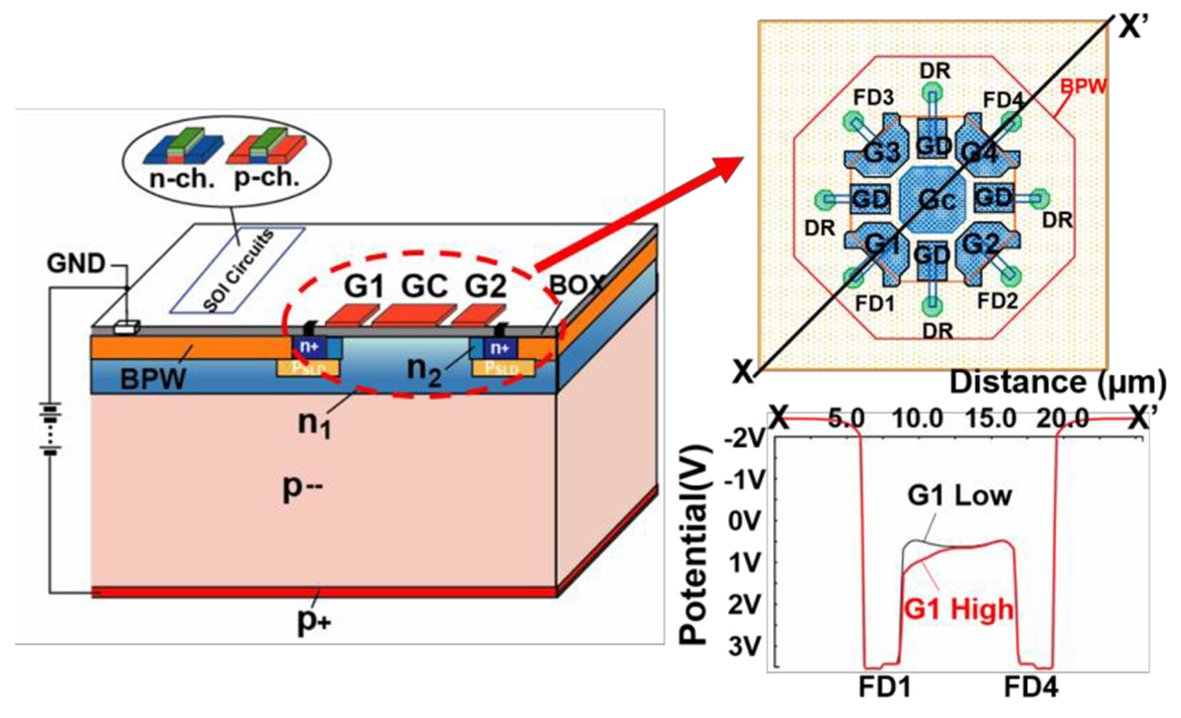
Figure 1 shows the proposed sensor structure and modulator layout with its potential diagram. In order to achieve a high QE at NIR region (at 950 nm), a thick substrate of 200 µm is used. Since the substrate has a lightly doping or high resistivity, the substrate bias of −30 V is supplied for fully depletion. The n-type doping, n1, creates a buried channel under the BOX. This layer is also used for preventing a punch-through hole current from the buried p-well (BPW) to the substrate. The channel potential is modulated by the SOI transfer gates (G1, G2, G3, G4, and GD), which are implemented by a highly-doped SOI layer formed on the BOX. The center gate (GC) is negatively biased to make the channel pinning. The p-type doping, P
SLD, creates a potential barrier so that a detected photon is not directly captured at a floating diffusion (FD). The generated electron is transferred from a buried channel to FD node by controlling gate bias.
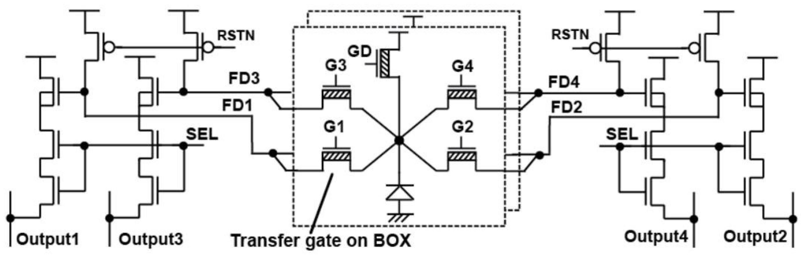
Figure 2 shows the pixel schematic of the prototype sensor. The pixel is composed of two charge modulators, a reset transistor (RSTN), a select transistor (SEL), and four source follower amplifiers followed by the column-parallel circuit to readout each gate output. The modulator size is 18 × 18 µm
2, and the pixel size is 36 × 18 µm
2.
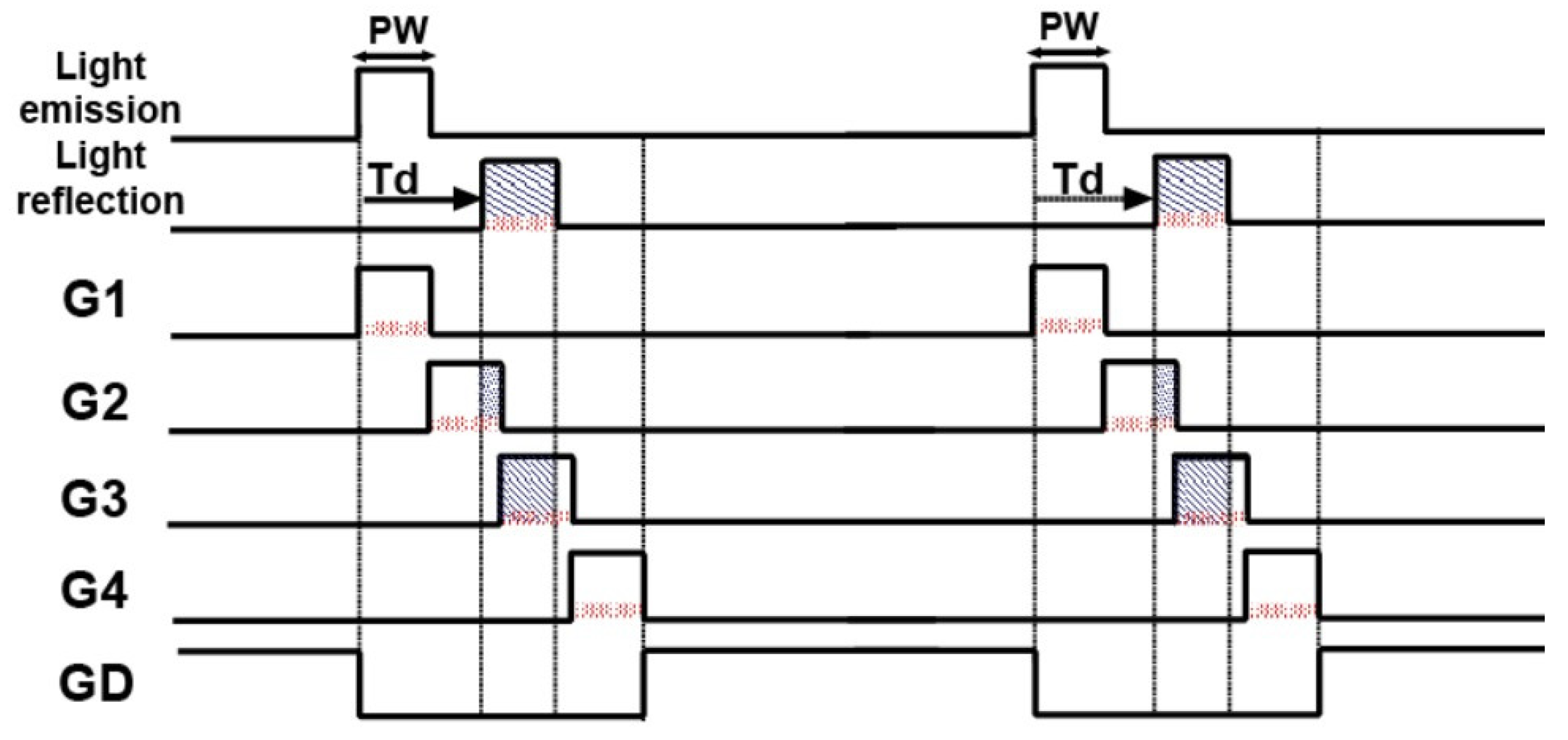
Figure 3 shows the timing diagram for the 4-tap lock-in pixel. The reflected short light signal is captured to the 4-tap outputs with 4 consecutive gate pulses. To suppress the background light, the GD is turned on after the signal capturing. The time of flight (Td) and the resulting distance is calculated in three-time windows (TW) by
where
DTW = 0.5cPw (c: velocity of light, Pw: gate width) and
N13 and
N24 are the differences from the first to third, and the second to fourth tapped signal outputs, respectively. Based on Equation (1), the measurable range of 3TW is obtained by a single frame. For further long range, the measurable range can be shifted by controlling a delay for gate modulation on sub-frame by sub-frame for obtaining a long-range 3D image in sufficiently high frame rate. This shifted short pulse modulation technique allows us to have high depth resolution while effectively suppressing the influence of the background light when compared to the continuous wave (CW) modulation.
3. Experimental Result
The prototype chip has been implemented in a 0.2 µm SOI-CMOS detector technology.
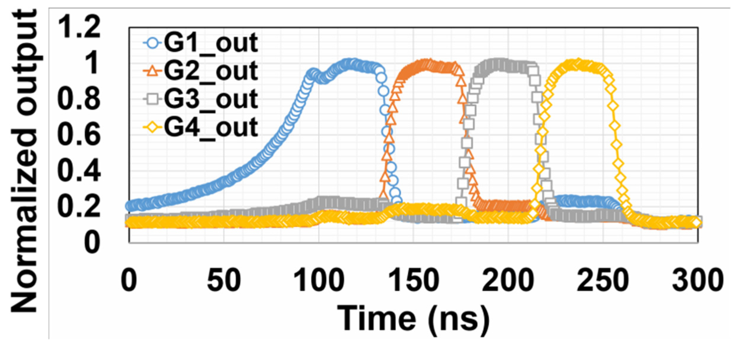
Figure 4 shows the measured 4-tap output with a short pulse laser (laser pulse width: 100 ps) of 930 nm wavelength. A high modulation contrast is achieved by using 4-tap lock-in pixel. Because the drain potential is not enough to drain, the output of G1 was gradually increased during the drain function.
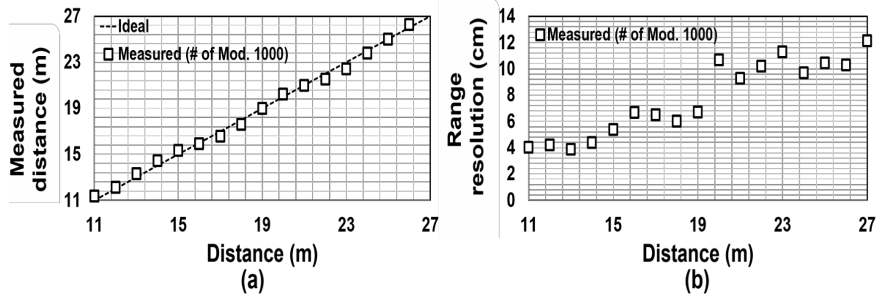
Figure 5a shows the relationship between the measured distance and the real distance, and
Figure 5b shows the range resolution which is the standard deviation in each distance with the step of 1 m at outdoor. A 950 nm laser, which has an average light power density of 150 mW/m
2 at 30 m and an optical bandpass filter of 950 nm (10 nm FWHM) are used. The background light condition is measured to be 100 klux on the top of the camera. The light and gate pulse is set to 40 ns, i.e., the measurable range is 18 m by using 3TW. The number of modulation pulses is repeated 1000 times. The measured distance linearity error is 1.5%, and the range resolution is measured to 12 cm at 27 m.
4. Conclusions
In this paper, a back-illuminated SOI based ToF image sensor has been developed and demonstrated for the LiDAR application. The proposed pixel structure was successfully detected NIR region (950 nm) with 200 µm thick bulk substrate. By using 4-tap lock-in pixel, the measurable range is improved 3 times rather than one tap structure in a single frame but also the range resolution is improved due to the background light canceling and draining function. The prototype ToF image sensor is measured high modulation contrast and a range resolution of less than 12 cm with strong background light for the range from 11 m to 27 m with 1.5% distance error.
