Proceeding Paper

Fabrication of a CMOS-based Imaging Chip with Monolithically Integrated RGB and NIR Filters †

Imec vzw, 3001 Leuven, Belgium
*
Author to whom correspondence should be addressed.
Presented at the Eurosensors 2018 Conference, Graz, Austria, 9–12 September 2018.
Proceedings 2018, 2(13), 751; https://doi.org/10.3390/proceedings2130751
Published: 8 January 2019
(This article belongs to the Proceedings of EUROSENSORS 2018)

Abstract

:
Recent developments in multispectral cameras have demonstrated how compact and low-cost spectral sensors can be made by monolithically integrating filters on top of commercially available image sensors. In this paper, the fabrication of a RGB + NIR variation to such a single-chip imaging system is described, including the integration of a metallic shield to minimize crosstalk, and two interference filters: a NIR blocking filter, and a NIR bandpass filter. This is then combined with standard polymer based RGB colour filters. Fabrication of this chip is done in imec’s 200 mm cleanroom using standard CMOS technology, except for the addition of RGB colour filters and microlenses, which is outsourced.

1. Introduction

Near infrared (NIR) imaging has many possible uses, ranging from defect inspection, medical diagnosis, and human-machine interaction to security/surveillance applications. In many cases, the NIR camera is combined with a second RGB camera to capture the colour information [1]. However, this comes at the cost of using 2 cameras, image registration and duplicating all down-stream image processing. This paper describes a combination of both functionalities onto a single image sensor, for the first time combining narrowband pixelated interference filters with traditional RGB polymer based colour filters. This is obtained by extending a classical RGB imager with a NIR sensitive pixel, enabling parallel acquisition of four channels [2]. The cost of the system is kept low by using standard, off-the-shelve CMOS sensors, standard CMOS technology for the integration of the filter stacks and the shield, and finishing with standard polymeric RGB colour filter processing. The monolithic integration also greatly reduces the size of the system compared to dual sensor approaches. To achieve good colour acquisition on the RGB channels, the inclusion of a NIR blocking filter at pixel level is crucial.
In this paper, we describe the idea of using a narrowband NIR filter and a NIR blocking filter for separation of the NIR signal from the visible light, in combination with RGB colour filters, and we describe the fabrication of the imaging chip.

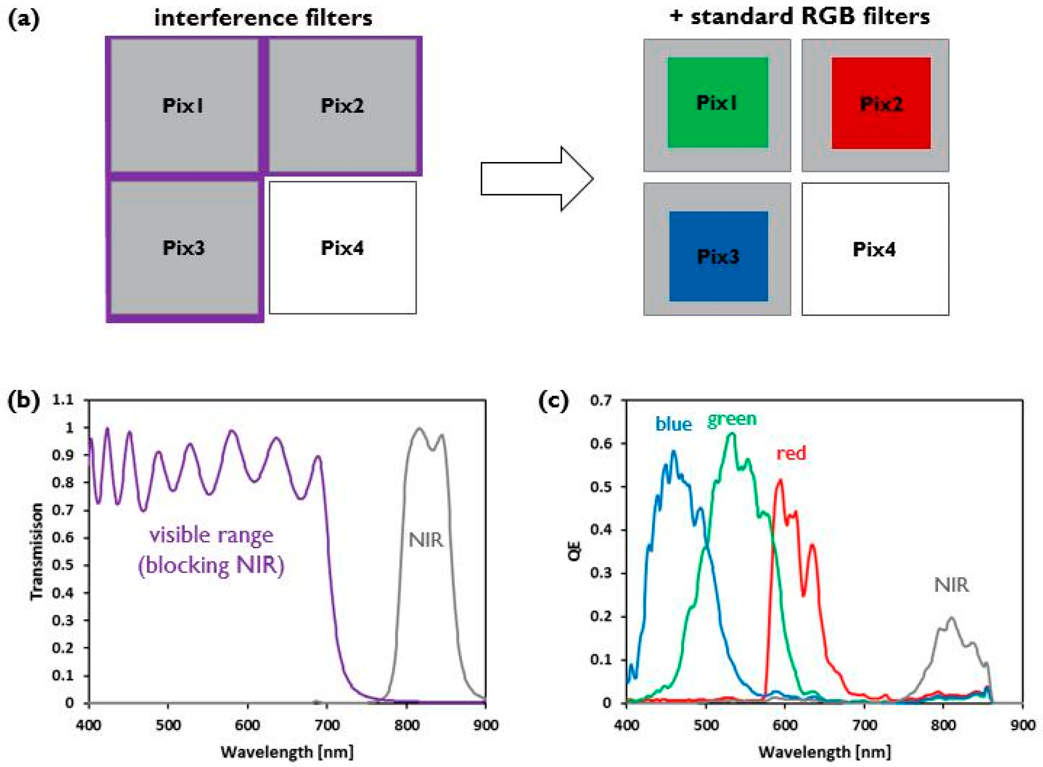
2. Combining NIR Block, Narrowband NIR, and RGB Filters

Other RGB + NIR imagers [3,4] add a fourth channel to the standard RGB pattern. However, the RGB channels are sensitive to the NIR signal. Signal separation is done by subtracting the NIR signal from the RGB channels using complicated algorithms. This results in a high signal to noise ratio in case of high intensity of the NIR light.
The imager described in this work uses a NIR blocking filter below the RGB pixels to physically separate visible and NIR signals. This is particularly important for applications that make use of artificial illumination, invisible to the human eye, to enhance the NIR signal without influencing the visible signal. This separation is difficult or impossible to achieve with polymeric filters only. Therefore, we combine, for the first time, interference filters for the visible and NIR separation with well-established polymeric colour filters for RGB colour separation. The NIR filter used is an interference based narrowband filter. The central wavelength and FWHM of the NIR bandpass filter can be tuned towards the spectral requirements of the application by changing the design.

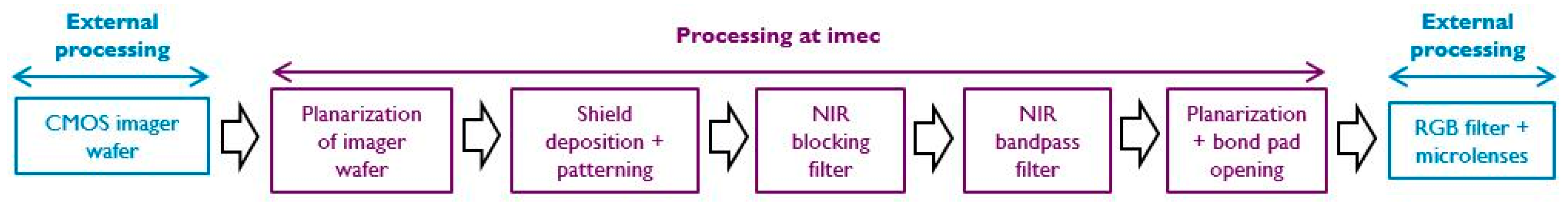
3. Overview of the Process Flow
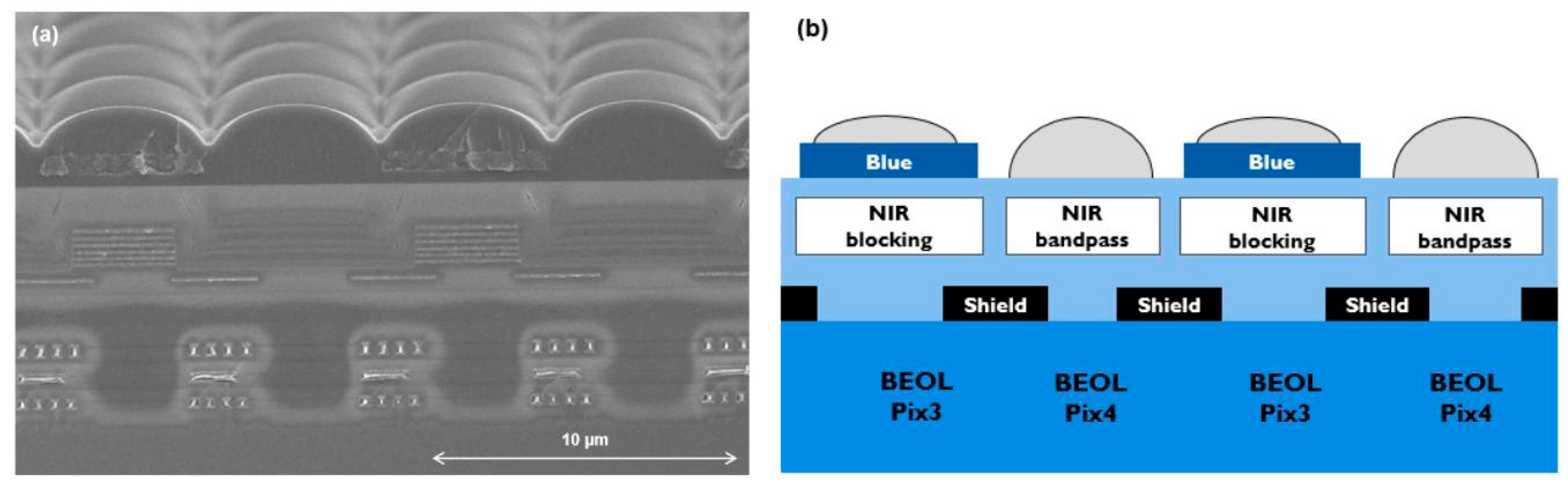
Figure 1 shows the schematic process flow, and Figure 2 a cross-section of the final product. The starting material is a commercial CMOS 200 mm imager wafer (CMOSIS CMV2000) with 2 MP and 5.5 um pixel size. Processing of the filter layers is done on top of this imager. Since the wafers have some topography, generated at the end of the BEOL processing, the first step is to planarize them, to allow the use of fine lithography further in the flow. We then proceed with the deposition and patterning of an embedded shield, followed by the deposition and patterning of the interference filters. We end with a final planarization, and then open the bond-pads again for electrical connection. All these steps are done in imec’s 200 mm cleanroom using standard CMOS technology tools and fabrication techniques. Lithography is used instead of the for imagers more commonly used lift-off technique, allowing smaller pixel patterning, and eliminating particle generation. Finally, the deposition of standard RGB colour filters and microlenses is outsourced.

4. Filters

Out of every four pixels, three are dedicated to visible light, and one to NIR (815 nm narrowband), as shown schematically in Figure 3. The distinction between red, green, and blue is made at the end of the processing, using traditional polymeric colour filters. Since these colour filters have leakage in the NIR range, leading to colour degradation, the first three pixels are covered by a NIR blocking filter, only allowing visible light to pass. The fourth pixel is covered by a NIR bandpass filter with 815 nm as central wavelength. Both interference filters are realized by deposition of dielectric multilayer stacks, followed by pixel level fine lithography, dry etch and photoresist strip; hence, classical CMOS compatible patterning techniques. Top view SEM and microscope images after processing the NIR blocking and bandpass filters are shown in Figure 4.

5. Shield

As can be observed in Figure 4, there is a transition region at the interface between the pixels, where the filter thickness is not well controlled. To avoid light passing through these areas onto the pixels, and create leakage, a metallic shield is deposited below the filters (Figure 2 and Figure 4b). The shield is fabricated by a thin metal layer deposition, optimized for the wavelength range of interest, and standard patterning. A clever design of this shield also allows to equalize the response over all wavelength intervals. The fill factor devoted to wavelength intervals with high sensitivity is reduced by increasing shield closure, while the one for low sensitivity wavelength intervals is kept as high as possible by enlarging the shield opening on the pixel [5].

6. Conclusions

In this paper, we have described the fabrication of a compact and low-cost spectral sensor, by monolithically integrating filters on top of commercially available image sensors. We have demonstrated the successful integration of a metallic shield to minimize crosstalk, and two interference filters: a NIR blocking filter, and a NIR bandpass filter. Standard 200 mm CMOS technology was used, combined with standard polymer based RGB colour filters and microlenses.

Author Contributions

B.V. and D.S.T. designed the manufacturing flow; B.V. performed the manufacturing; N.S., N.T. and A.L. designed filters and shield, executed and analyzed the spectral measurements; E.V.B. compiled the data and wrote the paper.

Acknowledgments

This work was conducted within the framework of the I-ALLOW European Project. We thank our colleagues Kenny Leyssens and Joris Ceuppens for the filter depositions, Vasile Paraschiv (Etch Tech Solutions) for the filter etch, Jesse Claes for SEM inspections, and imec’s Fab Operations team.

Conflicts of Interest

The authors declare no conflict of interest.

References

  1. Zhang, X.; Sim, T.; Miao, X. Enhancing photographs with Near InfraRed images. In Proceedings of the IEEE Conference on Computer Vision and Pattern Recognition, Anchorage, AK, USA, 23–28 June 2008. [Google Scholar] [CrossRef]
  2. Geelen, B.; Spooren, N.; Tack, K.; Lambrechts, A.; Jayapala, M. System-level analysis and design for RGB-NIR CMOS camera. Proc. SPIE 2017, 10110. [Google Scholar] [CrossRef]
  3. Chen, Z.; Wang, X.; Liang, R. RGB-NIR multispectral camera. Opt. Express 2014, 22, 4985–4994. [Google Scholar] [CrossRef] [PubMed]
  4. Teranaka, H.; Monno, Y.; Tanaka, M.; Okutomi, M. Single-Sensor RGB and NIR Image Acquisition: Toward Optimal Performance by Taking Account of CFA Pattern, Demosaicking, and Color Correction. Electron. Imaging 2016. [CrossRef]
  5. Tack, K.; Geelen, B.; Vereecke, B. HSI with Variable Fill Factor Per Spectral Band. EP Patent application No. EP3339821A1, 27 June 2018. [Google Scholar]
Figure 1. Schematic process flow.
Proceedings 02 00751 g001
Figure 2. Cross-section SEM image (a) and schematic cross-section (b) of the final chip.
Proceedings 02 00751 g002
Figure 3. Schematic of the filters on top of the pixels (a) and their spectral response (b, simulated & c, measured).
Proceedings 02 00751 g003
Figure 4. Tilted view SEM image (a) and top view microscope image (b) after interference filter processing.
Proceedings 02 00751 g004
Publisher’s Note: MDPI stays neutral with regard to jurisdictional claims in published maps and institutional affiliations.

