1. Introduction
MicroElectroMechanical Systems (MEMS) industry is nowadays dominated by silicon based technologies. They allow the production of considerably small and complex structures in very large amounts, compatible with the industrial scale production of accelerometers and sensors in general. On the other side, lithography based techniques present some drawbacks, as they require sophisticated and expensive equipment operating in cleanroom facilities thus limiting customizability and flexibility. Finally, a lack of tri-dimensionality, especially in the case of surface micromachining processes (see e.g., [
1]), leads the MEMS designer to deal with strict constraints during the design process of MEMS devices (e.g., accelerometers, gyroscopes). In this scenario, additive manufacturing (AM) technologies, like 3D printing, have emerged as a possible way to overcome the limitation of standard silicon micromachining processes for the production of the structures. In fact, complex 3D parts of virtually any shape can be physically created or rapidly modified directly from computer-aided design (CAD) files, thus enabling high product customization, overall process cost reduction and design versatility not limited by the usual constraints of the silicon manufacturing. Among all AM processes, stereolithography (SL) has mainly emerged as possible alternative to standard fabrication process in MEMS industry since it enables rapid manufacturing of high aspect-ratio micron-sized parts at high resolution (20–50 µm) (see e.g., [
2]).
In this work, a polymeric
z-axis accelerometer is fabricated by means of SL and wet metallization that provides surface conductivity, which is necessary to obtain a capacitive readout of the
z-axis accelerometer [
3]. The proposed device has dimensions in the order of hundreds of µm and constitutes a first step towards the realization of 3D printed accelerometers, which may represent an alternative to MEMS-based devices in applications where miniaturization is not mandatory while customization is desirable.
2. Mechanical Design and Fabrication Process
The proposed design consists in a square proof mass (4 mm × 4 mm × 2 mm) that is suspended through two flexural springs that allow the pure translational motion along the out-of-plane direction. The in-plane thickness of the springs is equal to 600 µm while the out-of-plane thickness is equal to 300 µm in agreement with the actual constraints for SL-printing high aspect ratio overhanged microstructures avoiding curling phenomena. At rest, the gap between the proof mass of the accelerometer and a fixed electrode is equal to 200 µm. When an external acceleration is applied along the z-axis direction, the inertial force acts on the proof mass that moves toward or away from the electrode. The displacement of the proof mass along the z-direction causes a capacitance variation between the electrode (kept at an electronic virtual ground) and the proof mass itself (biased with a test signal, as described later). The current flowing through this capacitance is directly proportional to its value, and thus enables a direct measurement of the acceleration-induced displacement. Modal analysis have been computed in COMSOL Multiphysics and the expected natural frequency of the out-of-plane mode of the accelerometer is equal to 233 Hz.
Accelerometers prototypes were built within 30 min with a SL machine model DWS028JPlus (Digital Wax Systems, DWS, Thiene, Italy) characterized by 22 µm (laser spot diameter) and 10 µm of lateral and vertical resolution, respectively. The apparatus is equipped with a monochromatic actinic laser source (Solid State Bluedge
®) with an emitting power of 30 mW at λ = 405 nm. Laser speed was ranged between 250 and 4300 mm/s, the layer thickness between 50 µm and 10 µm and a 20-µm hatching was set. 3D models were designed in Solidworks
TM CAD system and manufactured with DL260
® (DWS) commercially available resin (with Young’s modulus and density equal to 1.82 GPa and 1290 kg/m
3 respectively). In order to accomplish polymer conversion, the SL-printed models were post-cured for 15 min. Metallization of the samples has been performed employing a process already developed [
3]. After the application of a first electroless Cu layer of 0.5 µm, a second 1.5 µm layer of electrolytic Cu was deposited. Cu metallized 3D printed parts are, then, fixed to a Cu planar base. Two 100 µm PET sheets have been placed between the printed frame of the device (see
Figure 1a) and the Cu sheet (bottom electrode in
Figure 1a below) to provide electrical separation and a 200 µm air gap between the moving mass and the Cu base as required by the mechanical design of the accelerometer.
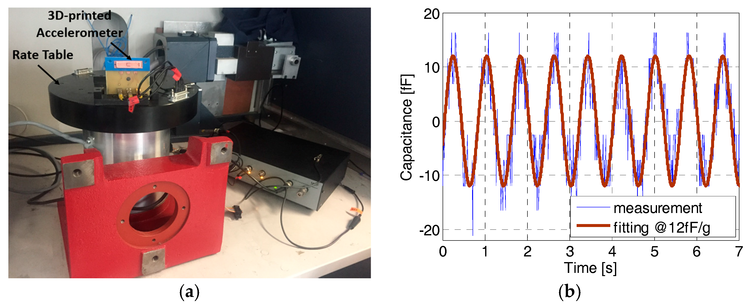
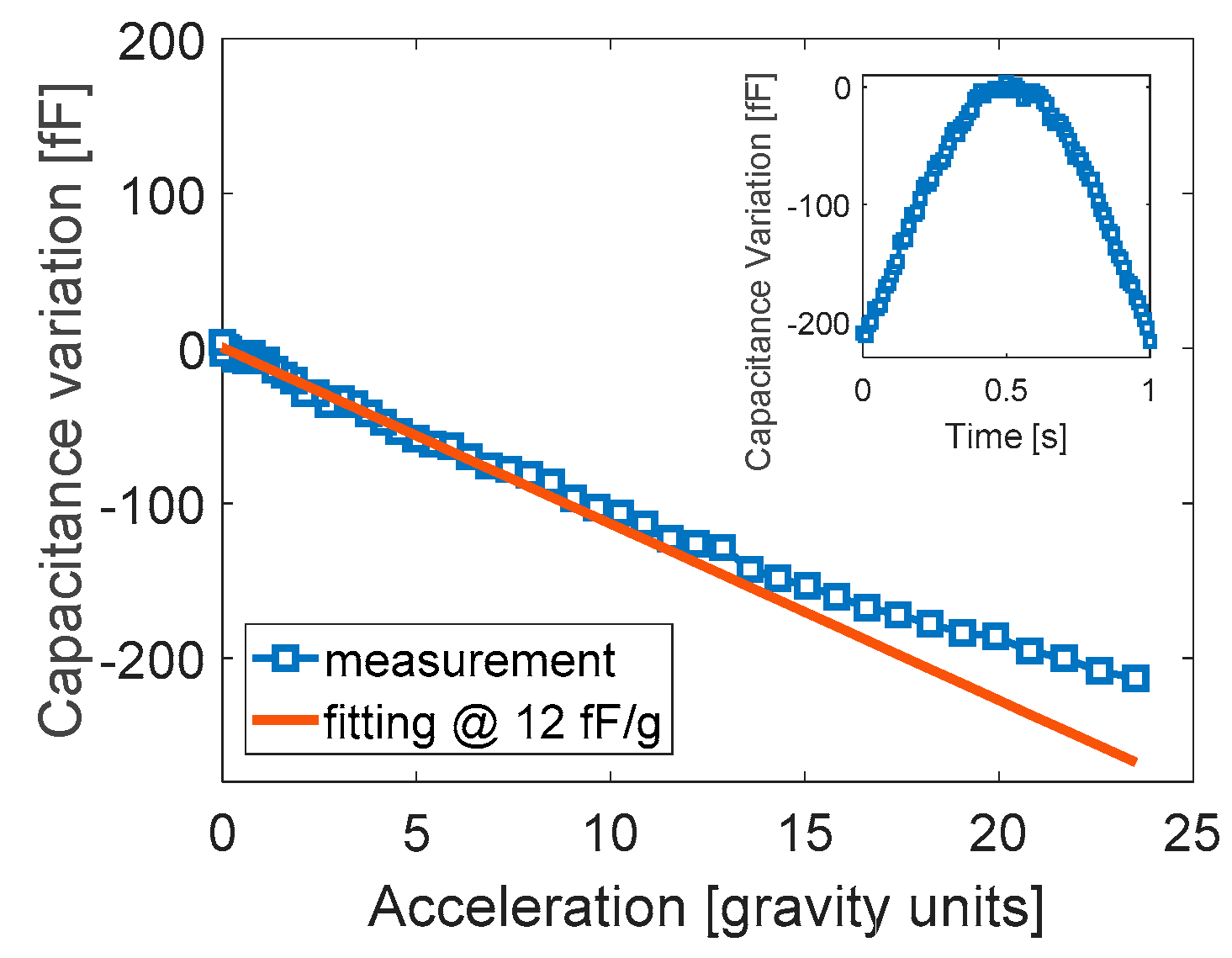
3. Experimental Measurements
The fabricated accelerometer shown in
Figure 1a was glued to a printed circuit board (PCB) and its two electrical contacts were wire bonded to pads on the PCB to allow capacitance measurements.
The first experimental characterization of the proposed device has been carried out through a MEMS Characterization Platform from ITmems srl, a tool specifically developed for testing of capacitive accelerometers and gyroscopes. First, a validation of the mechanical design parameters was performed using a ring-down measurement method: by applying a step force and monitoring the capacitance vs time behavior (see
Figure 1b), it is possible to evaluate the natural frequency and the quality factor of the accelerometer under test. Fitting the measured response gives a natural frequency of 230.4 Hz at a quality factor of about 15. Data are also crosschecked with a frequency domain fitting of the resonant peak in the corresponding FFT (see the inset in the same
Figure 1b). A good agreement between experimental data and theoretical prediction is thus found in terms of natural frequency. Note also how the quality factor lies in the typical range of actual, state-of-the-art, MEMS accelerometers. These preliminary experimental data can be considered as the first proof of the high reliability of the proposed design and fabrication process and of the feasibility of such kind of devices. Note that no unknown over or under etching must be taken into account during the design process of the accelerometer and this constitutes another distinctive advantage of the proposed fabrication process with respect to the classical MEMS fabrication.
Then, in-operation measurements were performed in order to evaluate the sensitivity ∆
C/
Ng (in terms of capacitance variation ∆
C per number of gravity units
Ng) of the proposed accelerometer, with the expected value, for the nominal gap
= 200 µm, area
= 16 mm
2 and measured angular frequency
= 2π·230 Hz, being given by:
and resulting nominally in 16 fF/g (g = 9.8 m/s
2 is here the gravity unit).
To measure the sensitivity, the PCB hosting the accelerometer was mounted on a rate table (AC1120 S from Acutronic) as shown in
Figure 2a, to exploit the centrifugal acceleration generated by its controlled motion at a radial distance from the center of 9 cm, and acting along the
z-axis (i.e., the sensing direction) of the 3D printed accelerometer. The capacitance measurement was still performed via the MCP, connected through the rate table sliding contacts to the PCB. In
Figure 2b, the capacitance measured at the bottom electrode as a consequence of a 1g-amplitude external acceleration (obtained by using the rate table in a flat horizontal position, with a slow rate and thus exploiting just gravity) is shown. By fitting the experimental curve, a sensitivity of 12 fF/g is obtained. Note that this value is on one side close to theoretical predictions, and on another side not far from typical performances of MEMS accelerometers usually in the order of 5–10 fF/g [
4]. The clearly visible huge quantization noise is due to the need of using small AC testing signals because of (i) the large parasitic capacitance introduced by the rate table sliding contacts and (ii) the parasitic induced by the non-optimized geometry of the sensing electrode in this prototypical demonstration. It is absolutely not an intrinsic limit of the accelerometer itself and it will be improved in future designs.
Finally, further measurements were performed using the rate table in the vertical arrangement shown in
Figure 2a, so to exploit large centrifugal accelerations up to 23.5 g, in order to check the linearity of the accelerometer response for large input signals. The measurement consists in applying a ramp of rising angular rates; as centrifugal acceleration is proportional to the square of the angular rate, one can expect a parabolic response measured between the capacitance electrodes. In
Figure 3, the capacitance variation measured at the bottom electrode as a function of the external acceleration is reported, after converting from rate to acceleration the actual parabolic result shown in the inset of
Figure 3. A good linearity error (< 3%) is achieved for accelerations up to 7 g, after which a predictable nonlinear effect given by single-ended, gap-opening induced nonlinearities become visible. The linearized sensitivity formula given above is indeed valid only for small displacements compared to the gap size, while the predicted proof mass motion at 23.5 g of acceleration is in the order of 109 µm. Differential structures, combining a pair of electrodes seeing opposite capacitance variations, are known to hugely mitigate nonlinearities and to cancel common mode noise. They are thus under consideration for future designs.