Article

Design and Analysis of Fractal-Shaped High-Impedance Surface Unit Cell Characteristics

by
Akash Kumar Gupta
1,
Harish Chandra Mohanta
1,*,
P. Satish Rama Chowdary
2,
M. Vamshi Krishna
3 and
Heba G. Mohamed
4,*
1
Department of Electronics and Communication Engineering, Centurion University of Technology and Management, Bhubaneswar 752050, India
2
Department of Electronics and Communication Engineering, Raghu Institute of Technology, Visakhapatnam 531162, India
3
Department of Electronics and Communication Engineering, Dhanekula Institute of Engineering and Technology, Vijayawada 521139, India
4
Department of Electrical Engineering, College of Engineering, Princess Nourah bint Abdulrahman University, P.O. Box 84428, Riyadh 11671, Saudi Arabia
*
Authors to whom correspondence should be addressed.
Fractal Fract. 2023, 7(6), 472; https://doi.org/10.3390/fractalfract7060472
Submission received: 3 May 2023 / Revised: 9 June 2023 / Accepted: 11 June 2023 / Published: 14 June 2023

Abstract

:
Fractal geometries consistently provide solutions to several electromagnetic design problems. In this paper, fractal geometries such as Hilbert and Moore curves are used to design efficient High-Impedance Surfaces. Modern communication devices have many sensors that are needed to communicate wirelessly. The critical component of wireless communications is antennas. Planar microstrip patch antennas are popular due to their low profile, compactness, and good radiation characteristics. The structural disadvantages of microstrip antennas are that they have surface waves that propagate over the ground plane. High-Impedance Surface (HIS) planes are a prominent solution to minimize and eliminate surface waves. The HIS structures behave as active LC filters that suppress surface waves at their resonance frequency. The resonance frequency of the structure is obtained by its LC equivalent or by analyzing the reflection phase characteristics. This work presents conventional HIS structures similar to mushroom HIS and fractal HIS such as Hilbert curve and Moore curve HIS. The HIS reflection phase characteristics are obtained by applying periodic boundary conditions with plane wave illumination. The results were obtained in terms of the reflection phase angle. The conventional mushroom structures show narrow band characteristics at given dimensions of 10 mm × 10 mm and 20 mm × 20 mm. These structures are helpful in the replacement of PEC ground planes for patch antennas under sub-6 GHz. The Hilbert and Moore fractals are also designed and have a multiband response that can be useful for L, S, and C band applications. Another design challenge of HIS is protrusions, which make design difficult. The work also presents the effect of having vias and the absence of vias on reflection phase characteristics. The response shows the least and no significant effect of vias under the x-band operation.

1. Introduction

In modern communications, antennas are integrated into the structure of devices or other objects to improve aesthetics, functionality, and performance. Day by day, the device size gets smaller, i.e., multiple sensors and other subcomponents are placed closer. Modern communications use microstrip patch antennas due to their versatile designs, low profile, and compactness. The patch antennas have good gain and radiation characteristics; however, these patch antennas suffer from surface wave radiation. The conventional patch antennas are structured with a Perfect Electric Conductor (PEC) ground plane followed by a thin substrate and radiating patch. The ground plane in patch antennas reflects the backward radiation in the forward direction, improving the gain. However, it carries image currents that result in lateral radiation and surface waves. The forward radiation and lateral surface wave radiation are shown in Figure 1a. In this scenario, when patch antennas are placed in a small footprint, it leads to multipath interference and mutual coupling, etc. To overcome these effects, High-Impedance Surfaces are a potential solution.
When PEC is used as the ground plane to produce constructive interference, the ground plane of the radiating patch must be placed around 0.25 λ . However, in practical applications, thin substrates have been used, and thickness is much less than 0.25 λ resulting in a destructive interference. The HIS as ground plane provides an in-phase reflection of the incident and reflected waves and creates a constructive interference even at thinner substrates ( λ ) . Thus, HIS improves the performance of the antenna.
High-Impedance Surfaces, often known as HISs, are a specific kind of surface that may be included in the design of antennas to boost their overall performance. In the HIS plane, a thin layer of small metal patches that are separated periodically are put over a ground plane. This arrangement constitutes an electromagnetic filter. The HIS helps to filter the number of surface waves that are reflected from the ground plane, which in turn helps to enhance the antenna’s overall efficiency. The radiation with eliminated surface waves is shown in Figure 1b. The radiation from the monopole placed over the PEC and HIS planes is shown in Figure 1. A wide range of different mushroom structures, cross, and other designed surfaces, can be utilized to produce the High-Impedance Structures. In comparison to more conventional antennas, HIS antennas provide several distinct benefits. Because they may be built to have a reduced profile, they are well suited for usage in applications in which there are small-size antennas designed by HIS and have been used successfully in a wide range of contexts, including wireless communication, radar, and satellite communications, amongst others.
The functional aspect of mushroom HIS is coined by Sivenpiper et al. [1]. The work incorporates the design of mushroom structures and lumped circuit analysis of its characteristics [2,3,4]. The conventional HIS mushroom is shown in Figure 2. It consists of small metallic patches that are periodically separated and soldered to the ground plane using vias. These connecting patches are referred to as protrusions. This arrangement constitutes a parallel lumped circuit capacitor and inductor. The periodically separated gaps between mushrooms are modeled as capacitors, while the connecting protrusions with the ground plane are modeled as an inductor. This shunted LC circuit models a filter that can eliminate surface waves at its resonance frequency. The LC equivalence model of HIS [2,3,4] is shown in Figure 2:
Z = j ω L e 1 ω 2 L e C e
where ‘z’ represents the sheet impedance, ‘ C e ’ stands for the capacitance, and ‘ L e ’ stands for the inductance. The HIS plane exhibits an inductive tendency at lower frequencies and a capacitive tendency at high frequencies as the frequency increases. As the impedance continues to increase, it eventually reaches an infinite value. The expression provides the resonance frequency:
ω 0 = 1 L e C e
ω ω 0 = L e / C e μ o ϵ 0
where ω is impedance bandwidth, and ω 0 is resonance frequency:
L e = μ r μ o t
C e = W ϵ 0 + ϵ 1 π cosh 1 l s
where ‘ ϵ 0 ’ is free space permittivity and ‘ ϵ 1 ’ is substrate permittivity.
Minu et al. [5] investigated the effect of vias on the resonant frequency of HIS and presented 3D altered vias to lower the resonant frequency without changing the thickness of the substrate. A HIS-based monopole antenna is presented in [6] for portable cell phone applications. The HIS plane is designed for metal islands having surface wave elimination at 2.4 GHz. The comparative performance of monopole antennas, when used with Electromagnetic Band Gap (EBG), PEC, and Perfect Magnetic Conductor (PMC), are ground planes presented in [7] and the HIS plane provides the best reflection coefficient. The work also proposed a Finite-Difference Time-Domain (FDTD) analysis of EBG and a proposed procedure to measure reflection phase characteristics. The spatial dispersive characteristics of HIS and homogenized methods to develop radiation characteristics are proposed in [8]. The fractals can minimize the antenna area due to their space-filling properties. Fractal antennas also have self-similar looping properties. The fractals have multiband properties that are directly related to the number of iterations that take place. In [9], the reflection phase characteristics of the Hilbert curve fractal for metamaterial formation are examined, the first time a monopole antenna is turned into a Hilbert curve shape and miniaturization is investigated [10]. The Hilbert fractals provided miniaturization with a dimension of 0.1 λ providing the same resonance as the 0.5 λ monopole used for VHF/UHF applications. The Hilbert curve-based reconfigurable antenna is presented [11], and reconfigurability is obtained by connecting RF switches within Hilbert fractals. In [12], the Hilbert curve fractal antenna for 2.42 GHz RFID applications is presented, providing 15.36–78.52% minimization. A Hilbert curve-based antenna is developed for gas-insulated switchgear (GIS) to detect particle discharge [13]. The multiband properties of Sierpinski fractal antennas are presented in [14]. The utility of fractal modeling has been demonstrated in [15] across multiple engineering applications. Fractal geometry is a valuable tool in the realm of antenna engineering, as it enables the design of compact and multi-frequency antennas and arrays, as well as high-gain elements. This paper provides a historical account of the prominent pioneers in fractal mathematics while highlighting the influence of fractal patterns on the development of antenna engineering. The work describes antenna geometries such as Mandelbrot, Sierpinski, Minkowski, Koch, Hilbert, Cantor, and Peano curves for antenna and wireless communication applications. The Moore curve-inspired antennas presented in [16] examine the multiband characteristics of antenna structures with improved bandwidths compared to those based on alternative space-filling geometries. The study has introduced expressions that establish a correlation between the parameters of an antenna slot and its primary resonant frequency and the succeeding resonant frequencies. In [17,18], the design of a hybrid fractal antenna (HFA) utilizing three widely recognized fractal curves is discussed: Koch, Minkowski, and Moore. The generator curve is produced using the combination of the Minkowski curve and the inverted Koch curve. The HFA is obtained by overlaying the hybrid generator curve onto the Moore curve. The study examines the effect of a defective ground and various substrates with different dielectric constants on an antenna’s performance [19,20]. This study involves the design of two distinct Moore antennas that differ solely in their microstrip transmission feedline forming split rings. It has been integrated with the Koch curve to enhance the multiband performance of the Moore antenna, resulting in improved bandwidth performance. The Hilbert curve fractal HIS for multiband band improved gain applications is presented in [21]. The prevailing discussion shows that fractal geometry-inspired antennas provide multiband characteristics, and HIS planes can potentially suppress surface wave propagation. The proposed work incorporates the integration of fractals into HIS planes. The work investigates the in-phase frequency response where the HIS plane has optimized performance to enhance the radiating properties of the radiating element. If the designer knows the HIS plane frequency response, he can design the radiating patch for desired applications for improved performance. Another design challenge associated with the HIS is that it has protrusions that link HIS patches to the ground plane. The work also investigates the effects of these vias on the reflection phase characteristics. A HIS-based antenna is shown in Figure 3.
The paper is organized into three sections, where the first section presents an introduction and short motivation and the literature. The second section discusses the design methodology for conventional mushroom HIS, slotted mushroom, Hilbert fractals, and Moore fractals. The third section describes the reflection phase characteristics of the designs.

2. Design Method

In this work, conventional mushroom HIS, slotted mushroom, and fractal HIS such as Hilbert curve fractals and Moore curve fractals have been designed. The HIS surfaces are designed and analyzed in a High-Frequency Structure Simulator.

2.1. Conventional Mushroom HIS

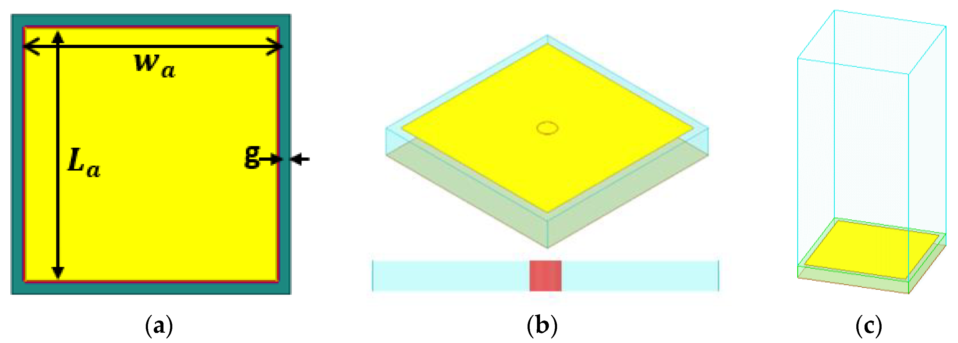
The conventional mushroom HIS cell is designed over an Fr4 substrate with a dielectric constant of 4.4 and a loss tangent of 0.02 [22]. The substrate thickness is 1.6 mm. The mushrooms being designed, namely mush10 and mush20, have dimensions ( L a × w a ) of 10   mm × 10   mm and 20   mm × 20   mm . The designed mushroom HIS cells are shown in Figure 4. The top view of the mushroom is shown in Figure 4a, Figure 4b shows the cross-section view, and the isometric view Figure 4c shows the radiation box.
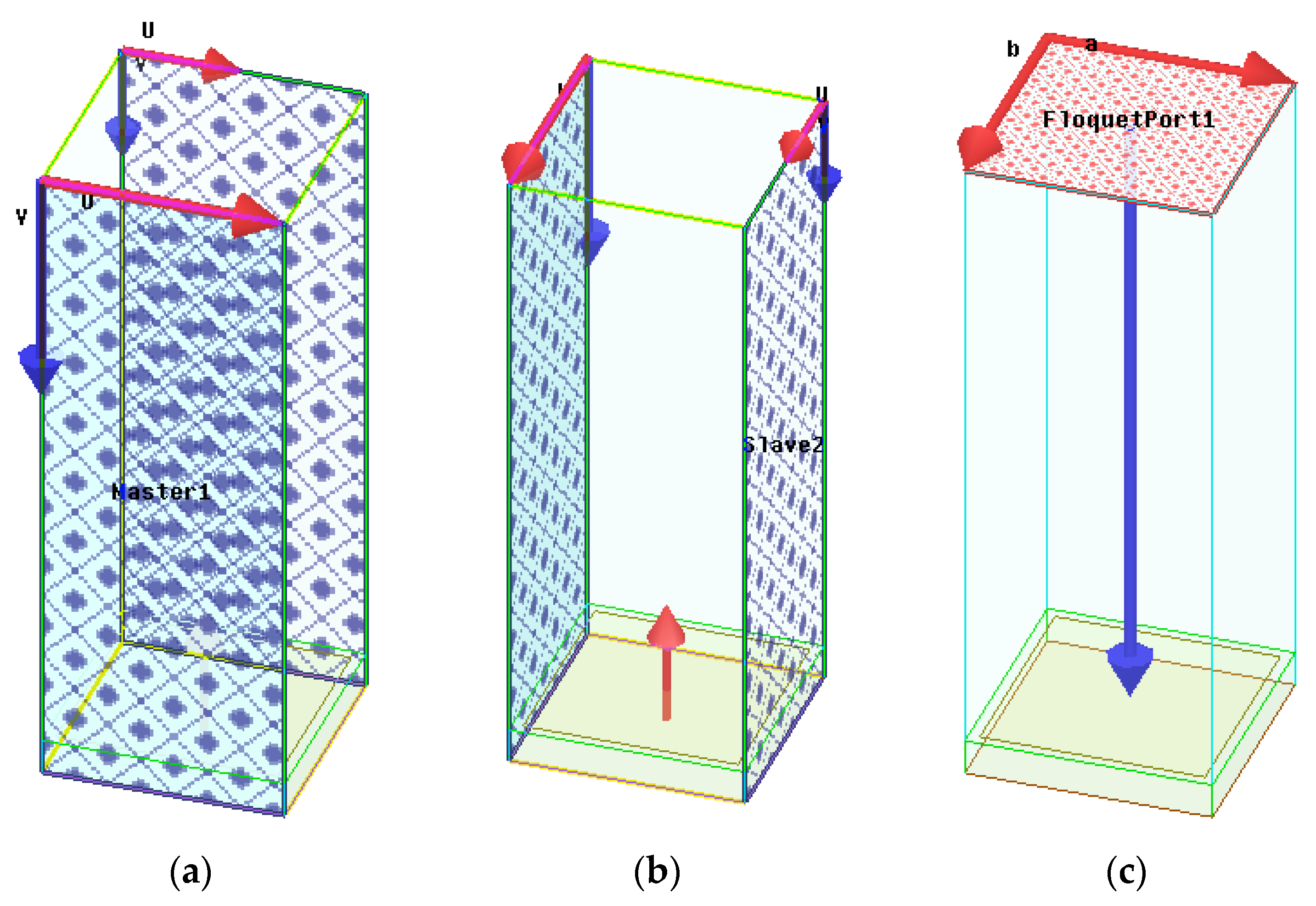
The simulation setup for a conventional mushroom structure is shown in Figure 5. The simulation setup uses periodic boundaries and plane wave illumination over the HIS surface. The utilization of the Finite-Difference Time-Domain (FDTD) method is demonstrated in Figure 5, wherein a plane wave model is employed to evaluate the reflection phase manifested by the High-Impedance Surface (HIS) interface. The FDTD method utilizes the total field/scattered field computation to incorporate plane wave excitation. A plane wave is introduced to illuminate the structure of the HIS consistently. The FDTD domain is split into the dispersed field area and the total field region by a virtual surface located at a distance of 0.40λ from the HIS bottom surface. A solitary unit of the High-Impedance Surface (HIS) configuration is employed to replicate an infinite periodic structure, with periodic boundary conditions (PBC) enforced on all four sides. The bottom surface of the HIS is located at a depth of 0.55λ beneath the perfectly matched layers (PML). It is not possible to ascertain the reflection phase by directly examining the reflected field at the top surface of the High-Impedance Surface (HIS) because the HIS structure is integrated within the overall field region. A plane of observation is positioned at a distance of 0.50λ above the bottom surface of the HIS, within the area of the dispersed fields, to capture the scattered fields from this plane for computing the reflection phase. Integrating the scattered fields over the observation plane is necessary to determine the reflected field emanating from the far-field region in the direction perpendicular to the surface. However, a correction of π is added to include reflection from the PEC plane. The HIS reflection phase characterization obtained from the process, as mentioned earlier, aligns with the characterization utilized in previous works, specifically in references [3,23,24]. To establish a methodology for utilizing the reflection phase curve to ascertain the frequency range of input match, it is possible to employ the simulation outcomes of a model featuring plane wave illumination.

2.2. The Slotted Mushroom HIS

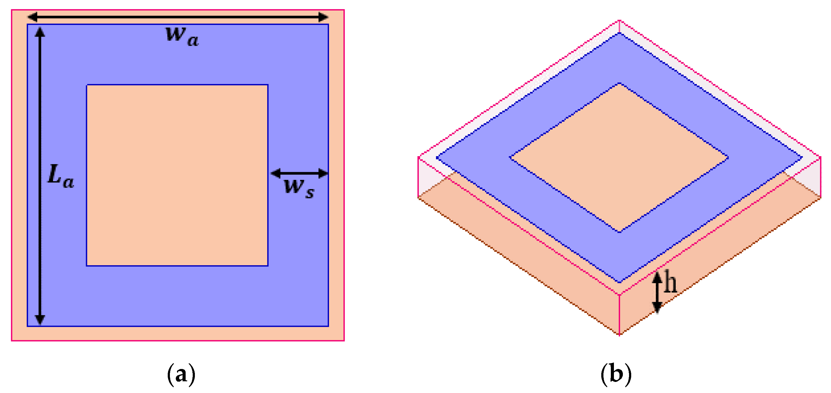
The slotted mushroom is designed on an FR4 substrate with a dielectric constant of 4.4 and a loss tangent of 0.02. The substrate thickness is 1.6 mm. The slotted mushroom outer square has dimensions ( L a × w a ) of 10   mm ×   10   mm . A square slot of 5 mm is made in the center patch. The designed slotted mushroom is shown in Figure 6. The slotted mushroom is simulated in periodic boundaries with plane wave illumination.

2.3. The Hilbert Curve Fractal HIS

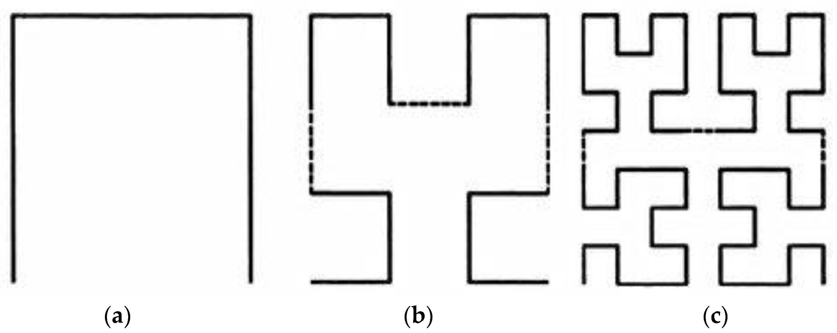
The Hilbert curves up to iteration 3 are shown in Figure 7. The Hilbert curve fractal-inspired HIS is designed on an FR4 substrate with a thickness of 1.6 mm. The square patch has a width of HILF10 ( L a × w a ) of 10   mm × 10   mm while for HILF20 it is ( L a × w a )   20   mm × 20   mm . The Hilbert curve width is 1 mm, and the gap between the unit cell is maintained at 2 mm. The designed Hilbert curve fractals up to the third iteration are shown in Figure 8. The designed Hilbert fractal-inspired HIS cells are simulated and analyzed in periodic boundaries with plane wave illumination.

2.4. The Moore Curve Fractal HIS

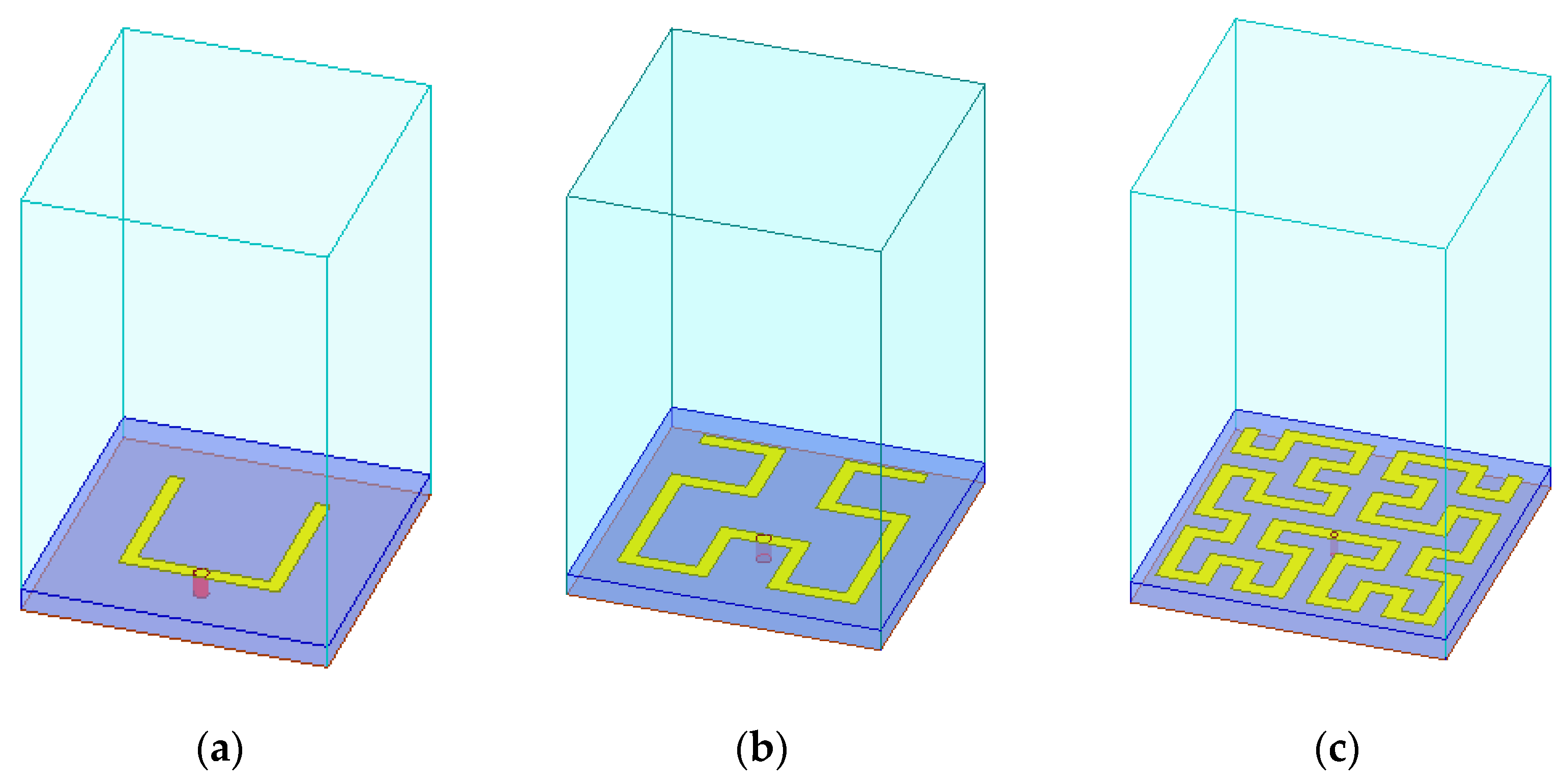
The Moore curves up to iteration 3 are shown in Figure 9. The Moore curve fractal-inspired HIS is designed on an FR4 substrate with a thickness of 1.6 mm. The square patch has a width for MooreF10 ( L a × w a ) of 10   mm × 10   mm while for MooreF20 it is ( L a × w a )   20   mm × 20   mm . The Moore curve width is 1 mm. The gap between the unit cell is maintained at 2 mm. The designed Moore curve fractals up to the third iteration are shown in Figure 10. The designed Moore fractal-inspired HIS cells are simulated and analyzed in periodic boundaries with plane wave illumination.
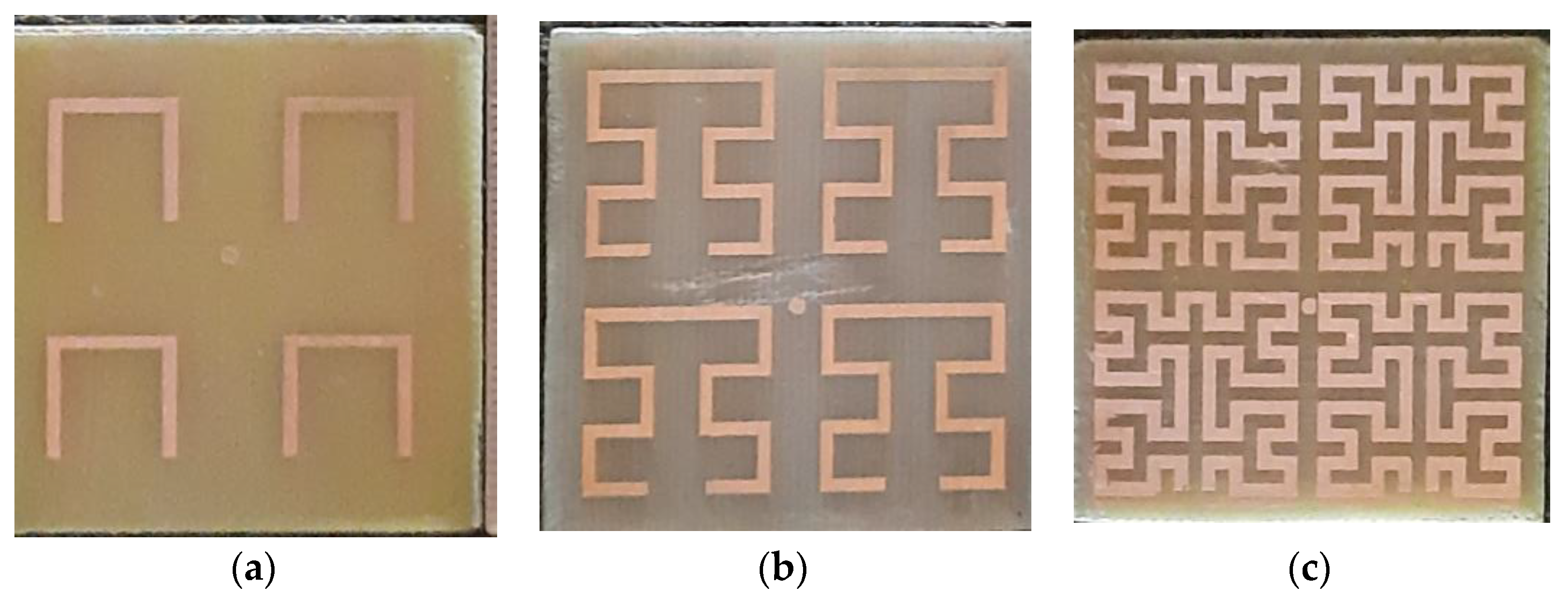
The Moore curve fractal HIS MooreF20 2 × 2 array is formed for multiband applications, as shown in Figure 11.

3. Results and Discussions

The various High-Impedance Surface unit cells are designed and analyzed in a High-Frequency Structural Simulator. The results are analyzed in terms of the reflection phase and ± π 2 matched impedance bandwidth of unit cells.

3.1. Conventional Mushroom HIS Cell

3.1.1. Lumped Circuit Analysis

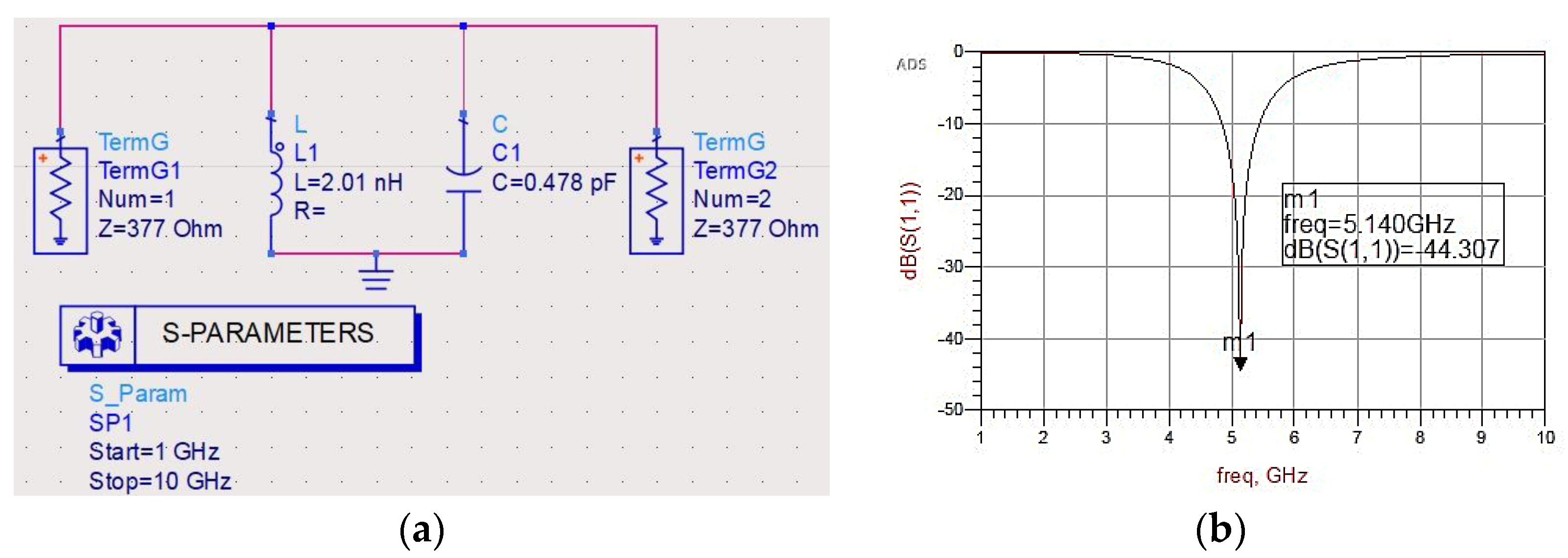
The conventional mushroom HIS is analyzed using LC lumped element circuit analysis. Using Equations (2)–(4), the mushroom with dimensions of La = Wa = 10 mm separated by 0.5 mm has an inductance of 2.01 nH/cell and capacitance of 478 fF/cell and a resonance frequency of 5.1 GHz. It has a bandgap bandwidth of 9% at the center frequency. The lumped equivalent circuit and reflection coefficient response are shown in Figure 12.

3.1.2. The FDTD Analysis

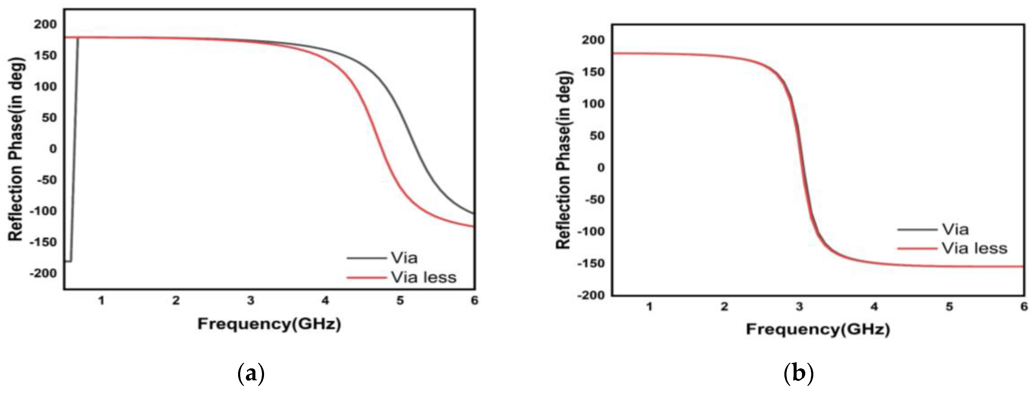
The Conventional mushroom’s mush10 and mush20 are analyzed using FDTD plane wave illumination. The reflection phase characteristics of mush10 and mush20 are shown in Figure 13, and the reflection phase response with and without via is presented.
The reflection phase characteristics of mush10 have zero-degree frequencies at 5.22 GHz with via and 4.86 GHz for the via-less structure. For mush20, zero-degree frequencies are at 3.06 GHz and 3.04 GHz for via and via-less HIS. The in-phase bandwidth of mush10 with via is in a range of 4.86–5.77 GHz, and via-less is in the range of 4.45–5.22 GHz. The in-phase bandwidth of mush20 with via is in a range of 2.93–3.22 GHz, with via-less in a range of 2.91–3.20 GHz. However, for mush10 in phase bandwidth with via and via-less the effect of via is marginal. The in-phase bandwidth for mush20 with via and via-less coincides and thus via has no effect for mush20. Concerning zero-degree frequency, the mush10 HIS can be used as the ground plane for enhancing performance for WiMAX, WLAN application patch antennas, and mush20 applications in C-band. The LC model analysis and FDTD solver resonant frequencies have good agreement. The parametric analysis is made for different lengths of mushrooms from 5 mm to 20 mm and the reflection phase response of mushroom unit cell with via is shown in Figure 14a and without via is shown in Figure 14b. The ± 90 ° bandwidth of HIS cells is shown in Table 1.

3.2. The Reflection Phase Characteristics of Slotted Mushroom

The reflection phase characteristics of the slotted mushroom are shown in Figure 15. The parametric analysis is also conducted for multiple slot width dimensions shown in Figure 15b. For the slotted mushroom-forming, a squaring with a width of 5 mm has a zero-degree frequency of 4.82 GHz shown in Figure 15a. The parametric analysis response for the slotted mushroom is presented in Table 2. It can be observed that as slot size decreases or ring width increases, the in-phase bandwidth increases. The maximum bandwidth is obtained at 0.83 GHz with a ring width of 8 mm.

3.3. The Hilbert Curve Fractal HIS Cell

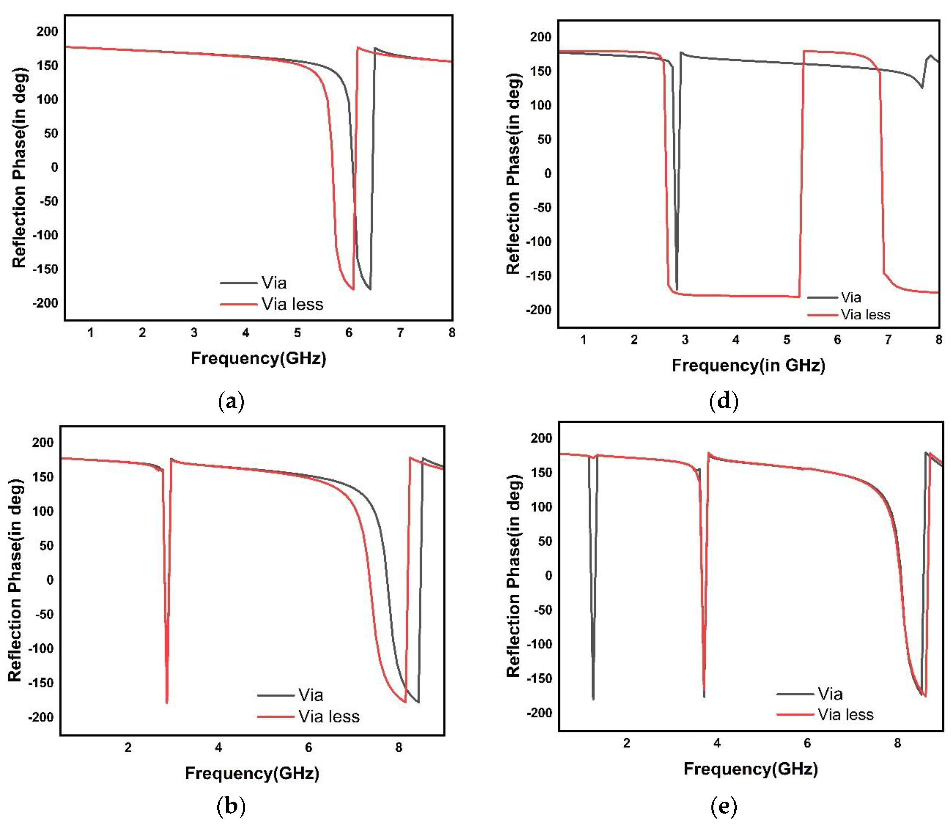
The reflection phase characteristics of HILF10 and HILF20 up to three iterations are shown in Figure 16. The reflection phase response of HILF10_1, HILF10_2, and HILF10_3 is shown in Figure 16a–c.
The zero-degree frequency of HILF10 iteration 1 with via is 6.07 GHz, and without via is 5.69 GHz. The zero-degree frequency of HILF10 iteration 2 with via is 2.81 GHz, 7.74 GHz, and without via is 2.81 GHz, 7.74 GHz. The zero-degree frequency of HILF10 iteration 3 with via is 4.48 GHz, 8.78 GHz, and without via has triple band frequencies centered at 1.63 GHz, 4.41 GHz, and 8.88 GHz. The in-phase ± 90 ° bandwidth is shown in Table 3.
The reflection phase response of HILF20_1, HILF20_2, and HILF20_3 is shown in Figure 16d–f. The zero-degree frequency of HILF20 iteration 1 with via is 2.79 GHz, and without via is 2.63 GHz. The HILF20 iteration 2 has a multi-frequency response with zero-degree frequencies with via at 1.21 GHz, 3.66 GHz, and 8.07 GHz, and without via at 3.66 GHz, 8.06 GHz. The HILF20 iteration 3 multi-frequency response with zero-degree frequencies with via is at 4.43 GHz, 8.49 GHz, and 9.93 GHz, and without via has triple band frequencies centered at 4.35 GHz, 8.49 GHz, and 9.90 GHz. The in-phase ± 90 ° bandwidth is shown in Table 4.
In the reflection phase characteristics of HILF10 and HILF20, it can be observed that there is a shallow effect of the presence of via, and in most cases the responses with and without via coincide. Thus, the effect of via on reflection phase response can be negligible.

3.4. Moore Curve Fractal HIS

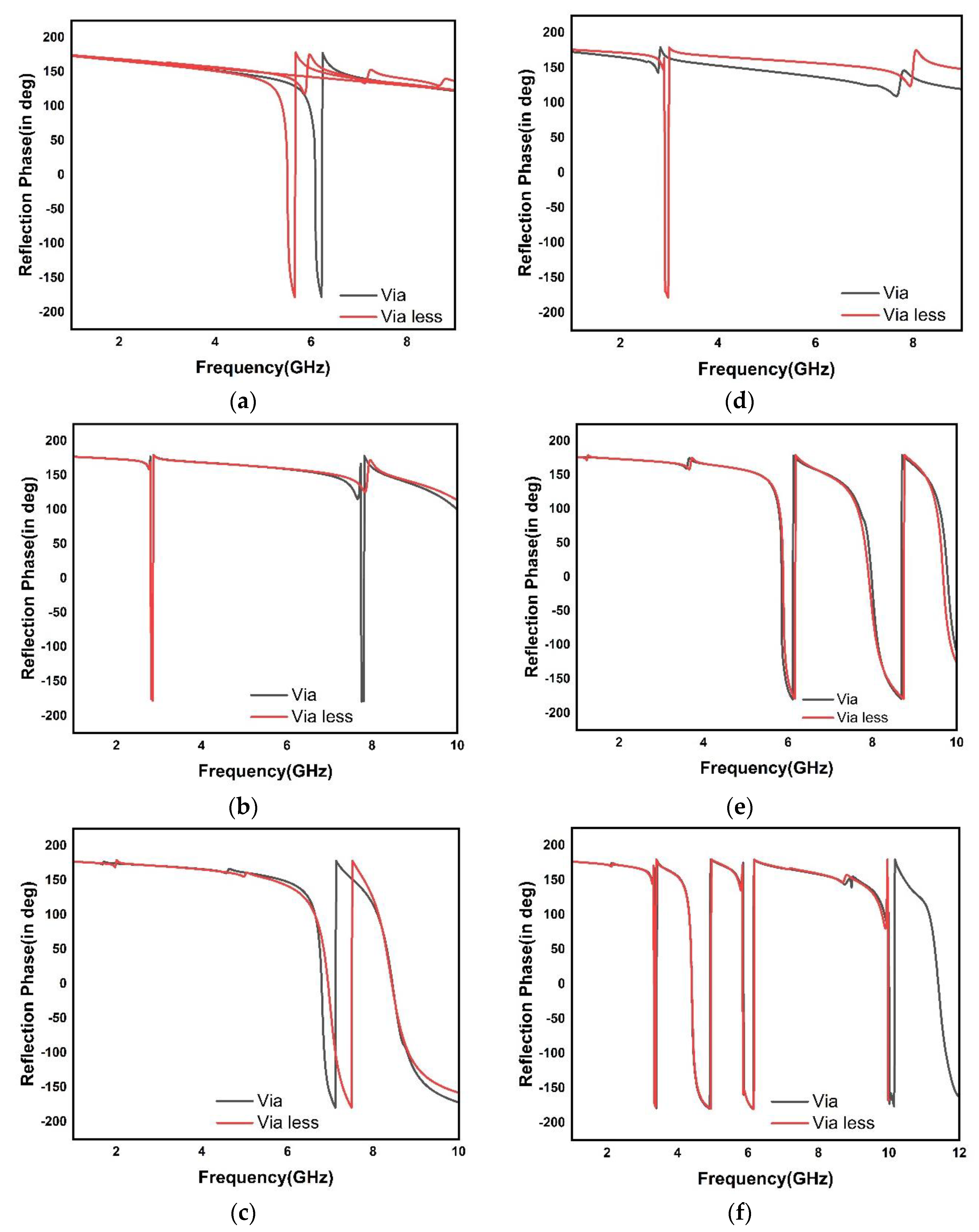
The reflection phase characteristics of MooreF10 and MooreF20 up to three iterations are shown in Figure 16. The reflection phase response of MooreF10_1, MooreF10_2, and MooreF10_3 is shown in Figure 17a–c.
The zero-degree frequency of MooreF10 iteration 1 with via is 6.09 GHz, and without via is 5.51 GHz. The zero-degree frequency of MooreF10 iteration 2 with via is 2.81 GHz, 7.74 GHz, and without via has a single band at 2.81 GHz. The zero-degree frequency of MooreF10 iteration 3 with via is 6.80 GHz, 8.45 GHz, and without via has dual-band frequencies centered at GHz, 6.95 GHz, and 8.44 GHz. The in-phase ± 90 ° bandwidth is shown in Table 5.
The reflection phase response of MooreF20_1, MooreF20_2, and MooreF20_3 is shown in Figure 17d–f. The zero-degree frequency of MooreF20 iteration 1 with via has no zero frequency under X-band, and without via is 2.91 GHz. The zero-degree frequency of MooreF20 iteration 2 with via has triple bands located at 5.85 GHz, 7.98 GHz, and 9.78 GHz; without via it has the triple band at 5.89 GHz, 7.92 GHz, and 9.68 GHz. The zero-degree frequency of MooreF20 iteration 3 with via has quadband frequencies located at 3.35 GHz, 4.40 GHz, 5.87 GHz, and 10.01 GHz, and without via has quadband frequencies centered at 3.33 GHz, 4.41 GHz, 5.85 GHz, and 9.97 GHz. The in-phase ± 90 ° bandwidth is shown in Table 6. The HIS planes find antenna applications WIMAX, WLAN, satellite uplink, and tank radar systems [25].

4. Conclusions

The work proposes using Fractal High-Impedance Surfaces to improve antennas’ gain and bandwidth performance. The work examines the effect of via on conventional mushrooms, slotted mushrooms, Hilbert curve, and Moore curve fractal HIS cells using FDTD solvers with plane wave illumination. The HIS structures provide an in-phase reflection of back radiation and suppress surface waves at their resonance frequency. The in-phase reflection frequency of the HIS structure is determined by calculating the reflection phase. The frequency corresponding to the reflection angle at 0 ° provides zero-phase reflection, and corresponding in-phase bandwidth is obtained at ± 90 ° frequency. The mushroom with side lengths of 5 mm, 10 mm, 15 mm, and 20 mm has an in-phase reflection at 1.8 GHz, 5.22 GHz, 3.85 GHz, and 3.06 GHz, respectively. The slotted mushroom with ring sizes of 4 mm, 5 mm, 6 mm, 7 mm, and 8 mm has an in-phase reflection at 4.56 GHz, 4.82 GHz, 5.06 GHz, 5.23 GHz, and 5.35 GHz, respectively. The Hilbert fractal HIS has in-phase reflection frequencies within the 1.63–10.03 GHz range. The Moore fractal HIS has a phase reflection coefficient in the range of 2.31–10.16 GHz. The investigations show that there is no significant effect of having via on reflection phase coefficients. The work could be extended by the design of planar antennas for desired applications using suitable HIS geometries.

Author Contributions

Conceptualization, A.K.G., H.C.M., P.S.R.C. and M.V.K.; methodology, A.K.G., H.C.M., P.S.R.C. and M.V.K.; validation, A.K.G.; formal analysis, H.C.M. and H.G.M.; investigation, H.C.M., P.S.R.C., M.V.K. and H.G.M.; resources, A.K.G. and H.C.M.; data curation, A.K.G.; writing—original draft preparation, A.K.G.; writing—review and editing, A.K.G., H.C.M., P.S.R.C., M.V.K. and H.G.M.; visualization, A.K.G., H.C.M., P.S.R.C., M.V.K. and H.G.M.; supervision, H.C.M., P.S.R.C. and M.V.K.; project administration, H.G.M.; funding acquisition, H.G.M. All authors have read and agreed to the published version of the manuscript.

Funding

Princess Nourah bint Abdulrahman University Researchers Supporting Project number (PNURSP2023TR140), Princess Nourah bint Abdulrahman University, Riyadh, Saudi Arabia.

Data Availability Statement

Not applicable.

Conflicts of Interest

The authors declare no conflict of interest.

References

  1. Sievenpiper, D.; Broas, R.; Yablonovitch, E. Antennas on high-impedance ground planes. In Proceedings of the 1999 IEEE MTT-S International Microwave Symposium Digest (Cat. No.99CH36282), Anaheim, CA, USA, 13–19 June 1999; Volume 3, pp. 1245–1248. [Google Scholar] [CrossRef]
  2. Sievenpiper, D.; Zhang, L.; Yablonovitch, E. High-impedance electromagnetic ground planes. In Proceedings of the 1999 IEEE MTT-S International Microwave Symposium Digest (Cat. No.99CH36282), Anaheim, CA, USA, 13–19 June 1999; Volume 4, pp. 1529–1532. [Google Scholar] [CrossRef]
  3. Sievenpiper, D.; Zhang, L.; Broas, R.; Alexopolous, N.; Yablonovitch, E. High-impedance electromagnetic surfaces with a forbidden frequency band. IEEE Trans. Microw. Theory Tech. 1999, 47, 2059–2074. [Google Scholar] [CrossRef] [Green Version]
  4. Wei, X.C.; Shu, Y.F.; Zhang, J.B.; Wang, D. Applications of high impedance surfaces for surface wave elimination. In Proceedings of the 2016 URSI Asia-Pacific Radio Science Conference (IEEE/URSI AP-RASC), Seoul, Korea, 21–25 August 2016; pp. 1458–1461. [Google Scholar]
  5. Gu, M.; Vorobiev, D.; Kim, W.S.; Chien, H.-T.; Woo, H.-M.; Hong, S.C.; Park, S.I. A novel approach using an inductive loading to lower the resonant frequency of a mushroom-shaped high impedance surface. Prog. Electromagn. Res. M 2020, 90, 19–26. [Google Scholar] [CrossRef] [Green Version]
  6. Broas, R.; Sievenpiper, D.; Yablonovitch, E. A high-impedance ground plane applied to a cellphone handset geometry. IEEE Trans. Microw. Theory Tech. 2001, 49, 1262–1265. [Google Scholar] [CrossRef]
  7. Yang, F.; Rahmat-Samii, Y. Reflection phase characterizations of the EBG ground plane for low profile wire antenna applications. IEEE Trans. Antennas Propag. 2003, 51, 2691–2703. [Google Scholar] [CrossRef] [Green Version]
  8. Costa, F.; Luukkonen, O.; Simovski, C.R.; Monorchio, A.; Tretyakov, S.A.; de Maagt, P.M. TE surface wave resonances on high-impedance surface based antennas: Analysis and modelling. IEEE Trans. Antennas Propag. 2011, 59, 3588–3596. [Google Scholar] [CrossRef]
  9. Mcvay, J.; Engheta, N.; Hoorfar, A.; Member, S. High Impedance Metamaterial Surfaces Using Hilbert-Curve Inclusions. IEEE Microw. Wirel. Compon. Lett. 2004, 14, 130–132. [Google Scholar] [CrossRef] [Green Version]
  10. Mahdi, M.A.; Abdullah, M.K.; Poopalan, P.; Ahmad, H.; Vinoy, K.J.; Jose, K.A.; Varadan, V.K.; Varadan, V.V.; Materials, A. Hilbert curve fractal antenna: A small resonant antenna for VHF/UHF applications. Microw. Opt. Technol. Lett. 2001, 29, 215–219. [Google Scholar]
  11. Vinoy, K.; Jose, K.; Varadan, V. Hilbert curve fractal antennas with reconfigurable characteristics. In Proceedings of the 2001 IEEE MTT-S International Microwave Symposium Digest (Cat. No. 01CH37157), Phoenix, AZ, USA, 20–24 May 2001; Volume 1, pp. 381–384. [Google Scholar]
  12. Murad, N.A.; Esa, M.; Yusoff, M.F.; Ali, S.H. Hilbert curve fractal antenna for RFID application. In Proceedings of the 2006 International RF and Microwave Conference, Putra Jaya, Malaysia, 12–14 September 2006; pp. 182–186. [Google Scholar]
  13. Wang, Y.; Wang, Z.; Li, J. UHF Moore Fractal Antennas for Online GIS PD Detection. IEEE Antennas Wirel. Propag. Lett. 2016, 16, 852–855. [Google Scholar] [CrossRef]
  14. Chowdary, P.S.R.; Prasad, A.M.; Rao, P.M.; Anguera, J. Design and Performance Study of Sierpinski Fractal Based Patch Antennas for Multiband and Miniaturization Characteristics. Wirel. Pers. Commun. 2015, 83, 1713–1730. [Google Scholar] [CrossRef]
  15. Anguera, J.; Andújar, A.; Jayasinghe, J.; Chakravarthy, V.V.S.S.S.; Chowdary, P.S.R.; Pijoan, J.L.; Ali, T.; Cattani, C. Fractal Antennas: An Historical Perspective. Fractal Fract. 2020, 4, 3. [Google Scholar] [CrossRef] [Green Version]
  16. Ali, J.K. A new microstrip-fed printed slot antenna based on Moore space-filling geometry. In Proceedings of the 2009 Loughborough Antennas & Propagation Conference, Loughborough, UK, 16–17 November 2009. [Google Scholar]
  17. Saraswat, R.K.; Kumar, M. Implementation of hybrid fractal metamaterial inspired frequency band reconfigurable multiband antenna for wireless applications. Int. J. RF Microw. Comput. Eng. 2020, 30, e22315. [Google Scholar] [CrossRef]
  18. Bangi, I.S.; Sivia, J.S. Minkowski and Hilbert curves based hybrid fractal antenna for wireless applications. AEU Int. J. Electron. Commun. 2018, 85, 159–168. [Google Scholar] [CrossRef]
  19. Bangi, I.S.; Sivia, J.S. Moore, Minkowski and Koch Curves Based Hybrid Fractal Antenna for Multiband Applications. Wirel. Pers. Commun. 2019, 108, 2435–2448. [Google Scholar] [CrossRef]
  20. Anguera, J.; Puente, C.; Martinez, E.; Rozan, E. The fractal Hilbert monopole: A two-dimensional wire. Microw. Opt. Technol. Lett. 2003, 36, 102–104. [Google Scholar] [CrossRef]
  21. Gupta, A.K.; Chowdary, P.S.R.; Krishna, M.V. Design of Rectangular Patch Antenna on the Hilbert Fractal-shaped High Impedance Surface. J. Sci. Ind. Res. 2023, 82, 202–209. [Google Scholar] [CrossRef]
  22. Gupta, A.K.; Satish Rama Chowdary, P.; Vamshi Krishna, M. High-Impedance Surface Backed Circular Patch Antenna for Wireless Communications. In Computer Communication, Networking and IoT. Lecture Notes in Networks and Systems; Satapathy, S.C., Lin, J.C.W., Wee, L.K., Bhateja, V., Rajesh, T.M., Eds.; Springer: Singapore, 2023; Volume 459. [Google Scholar] [CrossRef]
  23. Mosallaei, H.; Rahmat-Samii, Y. Broadband Characterization of Complex Periodic EBG Structures: An FDTD/Prony Technique Based on the Split-Field Approach. Electromagnetics 2003, 23, 135–151. [Google Scholar] [CrossRef]
  24. Yang, F.R.; Marchio, J.; Qian, Y.; Itoh, T. A Novel TEM-Waveguide Using Uniplanar Compact Photonic Band-Gap (UC-PBG) Structure. IEEE Trans. Microwave Theory Tech. 1999, 47, 2092–2098. [Google Scholar] [CrossRef]
  25. Terlapu, S.K.; Chowdary PS, R.; Jaya, C.; Sameer Chakravarthy VV, S.S.; Satpathy, S.C. On the design of fractal UWB wide-slot antenna with notch band characteristics. In Microelectronics, Electromagnetics and Telecommunications: Proceedings of ICMEET 2017; Springer: Singapore, 2018; pp. 907–912. [Google Scholar]
Figure 1. The Radiation (a) from the PEC Ground plane, (b) from HIS Ground plane.
Fractalfract 07 00472 g001
Figure 2. The Lumped Circuit equivalence of HIS plane.
Fractalfract 07 00472 g002
Figure 3. The HIS antenna.
Fractalfract 07 00472 g003
Figure 4. Mushroom HIS Cell (a) Top view (b) Isometric View (c) Radiation region.
Fractalfract 07 00472 g004
Figure 5. Simulation setup (a) PBC boundary 1 (b) PBC boundary 2 (c) Plane wave Incidence.
Fractalfract 07 00472 g005
Figure 6. The Slotted Mushroom unit cell (a) Top View (b) Isometric View.
Fractalfract 07 00472 g006
Figure 7. The Hilbert curve Fractal geometry (a) Iteration 1 (b) Iteration 2 (c) Iteration 3 iterations.
Fractalfract 07 00472 g007
Figure 8. The Designed Hilbert Curve Fractals (a) Iteration 1 (b) Iteration 2 (c) Iteration 3.
Fractalfract 07 00472 g008
Figure 9. The Moore Curve Fractals (a) Iteration 1 (b) Iteration 2 (c) Iteration 3.
Fractalfract 07 00472 g009
Figure 10. The Designed Moore Curve Fractals (a) Iteration 1 (b) Iteration 2 (c) Iteration 3.
Fractalfract 07 00472 g010
Figure 11. The prototype of 2 × 2 Moore Curve Fractal HIS (a) Iteration1 (b) Iteration 2 (c) Iteration 3.
Fractalfract 07 00472 g011
Figure 12. The LC model of mushroom cell (a) Simulated Circuit (b) Reflection Coefficient.
Fractalfract 07 00472 g012
Figure 13. The reflection phase characteristics (a) Mush10 (b) Mush20.
Fractalfract 07 00472 g013
Figure 14. The parametric analysis of Mushroom HIS (a) Unit cell with via (b) Unit cell without Via.
Fractalfract 07 00472 g014
Figure 15. The reflection phase characteristics (a) Slotted mushroom (b) Parametric Analysis.
Fractalfract 07 00472 g015
Figure 16. (a) HILF10_1 (b) HILF10_2 (c) HILF10_3 (d) HILF20_1 (e) HILF20_2 (f) HILF 20_3.
Fractalfract 07 00472 g016aFractalfract 07 00472 g016b
Figure 17. (a) MooreF10_1 (b) MooreF 10_2 (c) MooreF 10_3 (d) MooreF 20_1 (e) MooreF 20_2 (f) MooreF 20_3.
Fractalfract 07 00472 g017
Table 1. The In-phase bandwidth of Mushroom HIS Cell.
Dimension
(in mm)
With Via V = 0.5 mm
(Frequency in GHz)
Via Less
(Frequency in GHz)
0 ° + 90 ° 90 ° 0 ° + 90 ° 90 °
L P = W p = 5 1.831.811.85
L P = W p = 10 0.640.610.66
5.224.865.774.764.455.22
L P = W p = 15 3.853.654.123.853.654.12
L P = W p = 20 3.062.933.223.042.913.20
Table 2. Phase Bandwidth of Slotted Mushroom.
Ring Width
(in mm)

Frequency
(in GHz)
+ 9 0 °
Frequency
(in GHz)
9 0 °
Frequency
(in GHz)
Bandwidth
(in GHz)
44.564.334.780.45
54.824.545.100.56
65.064.725.390.67
75.234.845.620.78
85.354.935.760.83
Table 3. In-Phase bandwidth of HILF10.
Dimension
(in mm)
L P = W p = 10
With Via Radius V = 0.5 mm
(Frequency in GHz)
Via Less
(Frequency in GHz)
0 ° + 90 ° 90 ° 0 ° + 90 ° 90 °
HILF10_16.076.006.145.695.65.74
HILF10_22.812.792.842.812.792.84
7.747.527.887.357.127.51
HILF10_31.631.611.65
4.484.464.504.414.384.43
8.788.379.058.888.489.15
Table 4. In-Phase bandwidth of HILF20.
Dimension
(in mm)
L P = W p = 20
With Via Radius V = 0.5 mm
(Frequency in GHz)
Via Less
(Frequency in GHz)
0 ° + 90 ° 90 ° 0 ° + 90 ° 90 °
HILF20_12.792.772.812.632.602.65
HILF20_21.211.181.23
3.663.643.693.663.633.69
8.077.878.198.067.838.19
HILF20_34.434.404.464.354.324.37
8.498.338.588.498.348.55
9.939.8010.039.909.7310.01
Table 5. In-phase bandwidth of MooreF10.
Dimension
(in mm)
L P = W p = 10
With Via V = 0.5 mm
(Frequency in GHz)
Via Less
(Frequency in GHz)
0 ° + 90 ° 90 ° 0 ° + 90 ° 90 °
MooreF10_16.096.006.105.515.435.52
MooreF10_22.812.802.812.812.802.81
7.747.747.75
MooreF10_36.806.686.856.956.707.10
8.458.178.748.448.178.76
Table 6. In-phase bandwidth of MooreF20.
Dimension
(in mm)
L P = W p = 20
With Via V = 0.5 mm
(Frequency in GHz)
Via Less
(Frequency in GHz)
0 ° + 90 ° 90 ° 0 ° + 90 ° 90 °
MooreF20_12.912.902.92
MooreF20_25.855.805.865.895.825.91
7.987.758.117.927.78.08
9.789.639.939.689.559.83
MooreF20_33.353.343.353.333.333.38
4.404.354.454.414.354.45
5.875.855.875.855.835.86
10.019.9810.169.979.939.98
Disclaimer/Publisher’s Note: The statements, opinions and data contained in all publications are solely those of the individual author(s) and contributor(s) and not of MDPI and/or the editor(s). MDPI and/or the editor(s) disclaim responsibility for any injury to people or property resulting from any ideas, methods, instructions or products referred to in the content.