Article

Circuit Implementation of Variable-Order Scaling Fractal-Ladder Fractor with High Resolution

1
College of Computer Science, Sichuan University, Chengdu 610065, China
2
School of Physics and Engineering Technology, Chengdu Normal University, Chengdu 611130, China
3
College of Electronics and Information Engineering, Sichuan University, Chengdu 610065, China
*
Author to whom correspondence should be addressed.
Fractal Fract. 2022, 6(7), 388; https://doi.org/10.3390/fractalfract6070388
Submission received: 29 May 2022 / Revised: 8 July 2022 / Accepted: 10 July 2022 / Published: 12 July 2022

Abstract

:
Extensive research has been conducted on the scaling fractal fractor using various structures. The development of high-resolution emulator circuits to achieve a variable-order scaling fractal fractor with high resolution is a major area of interest. We present a scaling fractal-ladder circuit for achieving high-resolution variable-order fractor based on scaling expansion theory using a high-resolution multiplying digital-to-analog converter (HMDAC). Firstly, the circuit configuration of variable-order scaling fractal-ladder fractor (VSFF) is designed. A theoretical demonstration proves that VSFF exhibits the operational characteristics of variable-order fractional calculus. Secondly, a programmable resistor–capacitor series circuit and universal electronic component emulators are developed based on the HMDAC to adjust the resistance and capacitance in the circuit configuration. Lastly, the model, component parameters, approximation performance, and variable-order characteristics are analyzed, and the circuit is physically implemented. The experimental results demonstrate that the circuit exhibits variable-order characteristics, with an operational order ranging from 0.7 to 0.3 and an operational frequency ranging from 7.72 Hz to 4.82 kHz . The peak value of the input signal is 10 V . This study also proposes a novel method for variable-order fractional calculus based on circuit theory. This study was the first attempt to implement feasible high-resolution continuous variable-order fractional calculus hardware based on VSFF.

1. Introduction

Fractional calculus, a branch of mathematics, has been widely implemented in the various fields of science and engineering [1,2,3]. Although it typically has a constant order, its application in describing new phenomena and problems with an operational order dependent on variables such as time and space is difficult. These problems can be better described using variable-order fractional calculus [4,5,6], which was first proposed by Samko and Ross [7] in 1993. Variable-order fractional calculus is expressed through mathematical functions that can be used to model natural phenomena and processes. The studies conducted on variable-order fractional calculus were primarily focused on the mathematical description of variable-order phenomena and processes and on the theory of variable-order fractional calculus application system design [4,5,6,8,9,10,11,12]. However, studies on the implementation of flexible and controllable physical entities of variable-order fractional calculus are scarce.
The solid-state fractor can be used as the physical entity of variable-order fractional calculus operation. However, it faces certain limitations, such as a narrow range of operational order variation, limited temperature control, and difficulty in operational order adjustment [13,14]. Analog circuit implementation is an important approach that enables the flexible and controllable physical implementation of variable-order fractional calculus operation. Sierociuk et al. conducted several pioneering studies [15,16,17]. They use analog circuits to implement many kinds of variable-order fractional calculus circuits. These studies primarily employed the switching strategy to switch between two or three-order types. Constant-order fractor has been used in variable-order circuits and systems [15,16,17,18]. Variable-order fractional impedance (variable-order fractor) is a basic unit circuit or element that can perform variable-order fractional calculus. Variable-order fractional calculus can be realized by changing the operational order while maintaining the structure of the variable-order fractor circuit. In [19], a fractor circuit was designed based on rational approximation, and the order was changed by adjusting the transconductance operational amplifier control current. The operational order was switched between 0.2, 0.5, and 0.8; however, a physical circuit was not implemented. The studies conducted on variable-order fractor with a low operational order variation, narrow range, and regulation difficulties remain limited, to the best of our knowledge. Additionally, the studies conducted on circuit implementation are scarce.
To date, the studies conducted on fractor primarily focused on constant-order fractor circuits. These studies primarily involved two types of constant-order fractor [20]. The first type is constructed either directly or by modeling the phenomena of electrochemistry or other scientific fields, such as Liu-Kaplan [21], 2h-type fractal-tree [20], fractal-ladder [22,23], and fractal-chuan fractor [22,23,24]. The second type is constructed by designing a circuit-realizable rational function to approximate the performance of fractional-order operators such as the Oustaloup algorithm [25,26], Dutta Roy’s fractor [27], and Carlson’s iterating rational approximation algorithm [28,29].
In a previous study, we developed scaling expansion theory [30,31]. This theory can be used to extend multiple fractors, thereby overcoming the limitation of only realizing half- to arbitrary-order operations [30,32,33]. Scaling expansion theory can also be used in mathematics to extend the algebraic iterative equation, which describes the rational approximation of half-order operators into an irregular scaling equation describing arbitrary fractional operators. This theory can be used to construct the scaling fractal-lattice [30,31], scaling fractal-chuan [32], scaling fractal-chain [33], and scaling fractal-ladder fractor [34]. The scaling fractal fractor presents a high operating frequency bandwidth.
Scaling expansion theory is used to extend the semi-order fractor to a fixed scaling structure based on the required constant order. The theory is employed to realize the circuit of a fractional memristor of the scaling fractal-lattice [30] and scaling fractal-ladder fractor [34]. The lumped parameter value adjustment with the port flux or charge must be solved to achieve the scaling fractal fractional memristor [34]. It is similar to that the operational order adjustment must be solved to achieve the variable-order fractor.
Several studies have been conducted on scaling fractal fractor by using various structures [30,31,32,33,34]. However, the design of high-resolution emulator circuits to achieve high-resolution variable-order scaling fractal fractor is theoretically challenging. A variable-order scaling fractal-ladder fractor (VSFF) circuit implementation method is proposed to overcome this issue. The main contributions of this study are as follows:
  • The proposed circuit can realize the VSFF, thereby overcoming the limitations faced by the existing variable-order fractor, such as limited operational order variation, narrow range, and difficult adjustment [13,14,19].
  • A programmable resistor–capacitor series circuit and programmable universal electronic component emulators are designed based on the high-resolution multiplying digital-to-analog converter (HMDAC). These emulators can also be applied to other variable-order fractor circuits, memristor emulators, and memcapacitor emulators [35,36,37].
  • This paper also proposes a method for variable-order fractional calculus based on circuit theory.
The remainder of this paper is organized as follows. Section 2 presents the VSFF circuit configuration. A programmable resistor–capacitor series circuit emulator and a universal electronic component emulator are designed based on the requirements of the circuit configuration. Section 3 presents the model and component parameters in the VSFF and the calculation of the relative error of equivalent parameters of the programmable circuit. The approximation performance and variable-order characteristics of the VSFF are analyzed in the frequency domain. The VSFF is implemented, and the variable-order operation characteristic of the circuit is experimentally validated. Section 4 and Section 5 present the discussions and conclusions, respectively.

2. VSFF Design

This section describes the design of the proposed VSFF. Firstly, the circuit configuration is presented. Subsequently, the emulators required to realize the programmable resistor–capacitor series circuit, universal electronic capacitor, and resistor components are described.

2.1. VSFF Circuit Configuration

Scaling fractal-ladder fractor is a classic constant-order fractor circuit [34]. It is employed to achieve the scaling fractal fractional memristor and design the lumped parameter value of the fractor with the port flux or charge [34]. Similarly, the constant-order fractor circuit component parameters must be adjusted based on the required change in the operational order to design a variable-order fractor circuit for solving the problem. Therefore, the design of the VSFF circuit configuration requires only the resistor and capacitor to be replaced in the constant-order scaling fractal-ladder fractor with the variable resistor and capacitor controlled by the microcontroller.
This subsection presents the VSFF circuit configuration and explains the parameters and calculation of the admittance function. Subsequently, the equivalent operation order expression of the VSFF in the characteristic frequency range is calculated to prove that the VSFF possesses characteristics of variable-order fractional calculus operations. Furthermore, it presents a method to optimize the VSFF and improve the approximation performance. Lastly, it explains the correlation between the circuit parameters and operation order.

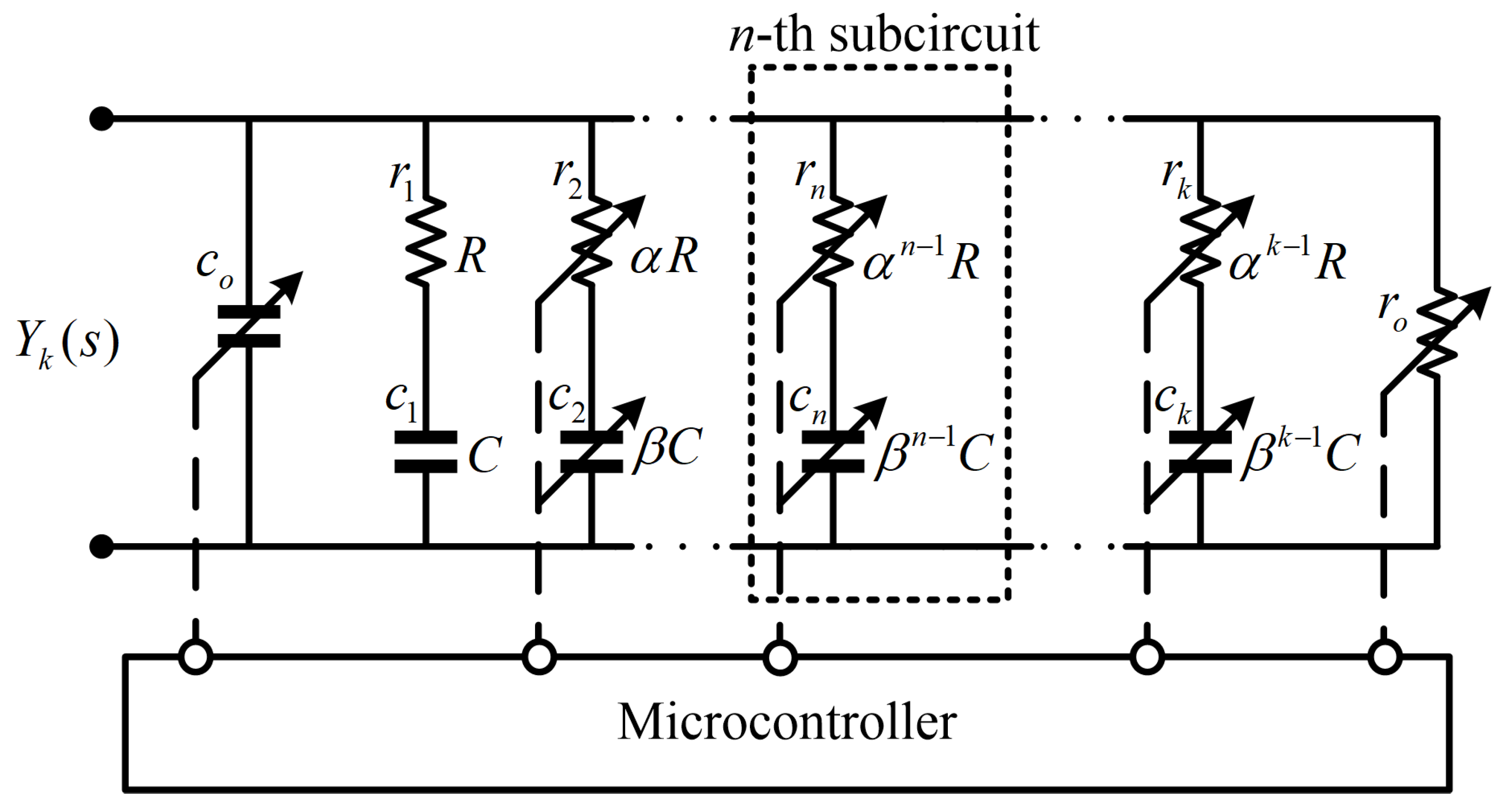
2.1.1. Circuit Configuration and Admittance

Figure 1 depicts the VSFF circuit configuration. The n-th subcircuit comprises a variable resistor, r n , in series with a variable capacitor, c n . k denotes the total number of subcircuits. The serial number, n = 1 , 2 , , k . R ( C ) , denotes the reference resistance (capacitance). Resistor r o and capacitor c o are used for circuit optimization. The n-th subcircuit, r o , and c o denote the programmable resistor–capacitor series circuit, programmable resistor, and programmable capacitor emulators, respectively, which are controlled by the microcontroller. α ( β ) denotes the resistance (capacitance) progression ratio. The parameter [15,31],
σ = α β ( α R + , β R + , 0 < δ 1 )
represents the scaling factor of the circuit, where α , β , and σ denote the scaling parameters. The scaling parameters are positive real numbers and α 1 , β 1 . The case in which all the scaling parameters are greater than 1 corresponds to the direct proportion extension VSFF. However, the case in which all the scaling parameters are between 0 and 1 corresponds to the inverse proportion extension VSFF.
The VSFF can realize any real fractional operation in the approximation frequency range. When resistor r o and capacitor c o are not considered, the admittance of the VSFF function can be obtained as follows:
Y k ( s ) = 1 Z ˜ k ( s ) = n = 1 k β n 1 C s 1 + σ n 1 R C s ,
s denotes the Laplace or the operational variable, where τ = R C , w = τ s , and Y ¯ k ( w ) = Y k ( w / τ ) R . The admittance function is normalized as follows:
Y ¯ k ( w ) = n = 1 k β n 1 w 1 + σ n 1 w .
The iterative algorithm formula of the normalized admittance function is expressed as follows:
Y ¯ k ( w ) = w 1 + w + Y ¯ k 1 ( σ w ) α .
When k + , the equation,
y ¯ ( w ) = w 1 + w + y ¯ ( σ w ) α
corresponding to the formula of the iterative algorithm, which is the VSFF scaling equation. Equation (5) can be used to analyze the electrical characteristics of the VSFF, including the frequency characteristics and operational order.

2.1.2. Characteristic Frequency and Operational Order

The theoretical expression of the operational order of VSFF in the characteristic frequency range can be calculated. The characteristic frequency of the n-th subcircuit can be expressed as follows:
ω n = 1 α n 1 β n 1 = σ 1 n ( n = 1 , 2 , k ) .
Therefore, when 1 < σ < is a direct proportion extension, ω n is extended to the lower-frequency range. In an inverse proportion extension, 0 < σ < 1 , ω n is extended to the higher-frequency range. When
1 < σ < + , ω k ω 1 = 1 ,
at high frequencies ( 1 < | ω | ), the circuit exhibits resistive characteristics. At low frequencies ( 1 > | ω | 0 ), the circuit exhibits capacitive characteristics, that is
0 1 β k 1 β · w 0 | ω | < 1 Y ¯ k ( w ) 1 < | ω | 1 α k 1 α 1 .
When the frequency band meets
0 ω k < | ω | 1 ,
the resistive and capacitive components interact, and the circuit exhibits fractional calculus operational performance. The operational order can be expressed as follows [34]:
μ lg α lg σ = lg α lg α + lg β ,
where μ denotes the operational order. A VSFF can be constructed by adjusting the values of α and β , as shown in (10).

2.1.3. VSFF Optimization

The parallel-connected resistor, r o , and capacitor, c o , in the circuit are used to optimize the VSFF to achieve a better variable-order fractional calculus performance. It is assumed that an infinite number of subcircuits exist before the 1-th subcircuit and behind the k-th subcircuit since the total number of subcircuits is limited. When α , β > 1 . The resistance and capacitance decrease progressively with decreasing number of n at each subcircuit before the 1-th circuit. The capacitor of each subcircuit plays a significant role. The capacitor connected in parallel before the 1-th subcircuit is expressed as follows:
c o = n = 1 β n C = C β 1 ( β > 1 ) .
For each subcircuit behind the k-th circuit, both the resistance and capacitance increase with increasing number of n. The resistor of each subcircuit plays a significant role. The resistor connected in parallel behind the k-th subcircuit is expressed as follows:
r o = 1 n = k 1 / ( α n R ) = ( α 1 ) R α 1 k ( α > 1 ) .
Similarly, when 0 < α , β < 1 , the capacitor connected in parallel before the 1-th subcircuit and the resistor connected in parallel behind the k-th subcircuit are β k C 1 β and ( 1 α ) R α , respectively.
Without loss of generality, the VSFF circuit uses a direct proportion extension ( α , β > 1 and σ > 1 ).

2.1.4. Component Parameter Calculation

The parameter values of each component and its variation rule of the circuit configuration can be calculated based on the operational order, μ , and its variable-order range. μ min and μ max denote the minimum and maximum values of the variable-order range, respectively. The resistance progressive ratio, α = σ μ , and capacitance progressive ratio, β = σ α = σ μ + 1 , are calculated based on the variable-order range, 1 < μ min μ μ max < 0 , and scaling parameter, σ . The n-th variable resistor,
r n = R α n 1 = R σ ( 1 n ) μ ,
and the n-th variable capacitor,
c n = C β n 1 = C σ ( n 1 ) ( μ + 1 ) .
The resistor,
r o = ( α 1 ) R α 1 k = 1 α 1 α k R = 1 σ μ σ μ k R ,
and the capacitor,
c o = C β 1 = C σ μ + 1 1 .
The partial derivative of the n-th variable resistor r n with respect to the operational order μ can be obtained as follows:
r n μ = ( 1 n ) R σ ( 1 n ) μ ln σ .
If n = 1 , r n μ = 0 . If n = 2 , 3 , , k ,
r n μ < 0 .
The resistance of r n decreases with an increase in μ apart from the fixed value of r 1 . The partial derivative of c n corresponding to μ can be obtained as follows:
c n μ = ( n 1 ) C σ ( n 1 ) ( μ + 1 ) ln σ .
If n = 1 , c 1 μ = 0 . If n = 2 , 3 , , k ,
c n μ > 0 .
Except for the fixed value of c 1 , the capacitance of c n increases with an increase in μ .

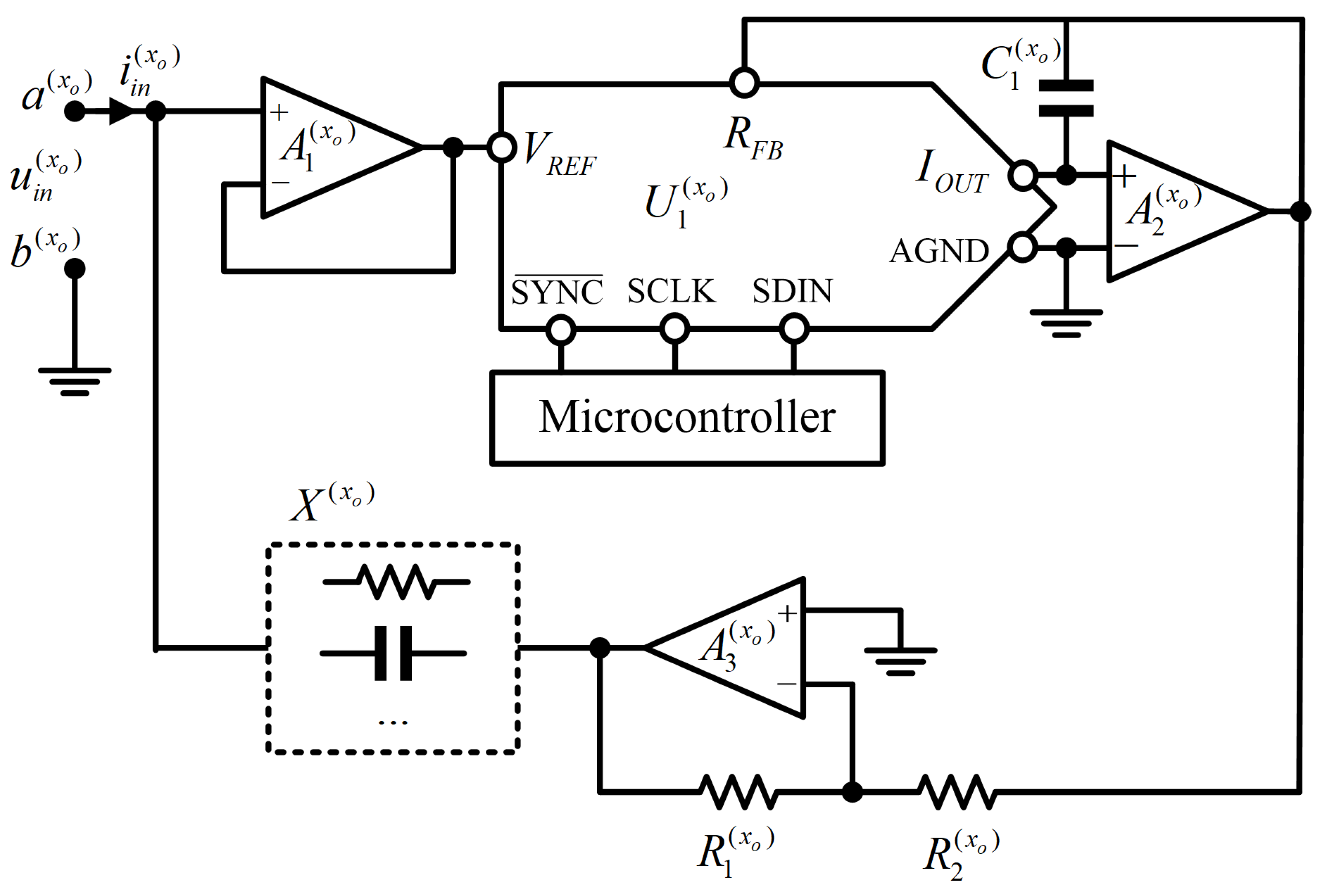
2.2. Programmable Resistor–Capacitor Series Circuit Emulator

Figure 1 depicts the n-th subcircuit, which is composed of a variable resistor, r n , in series with a variable capacitor, c n . If the variable resistor, r n , and variable capacitor, c n , are equivalent when using separate emulators, each emulator must be controlled separately, and the variable capacitor emulator circuit must be operated by floating. The n-th programmable resistor–capacitor series circuit emulator ( n = 2 , 3 , , k ) was designed to avoid using more hardware circuits and separately control each emulator. r n and c n can be controlled by a single HMDAC, and a separate floating emulator circuit is not required.
This subsection presents the circuit schematic of the programmable resistor–capacitor series circuit emulator and explains the parameters involved. The theory proves that the circuit schematic can achieve the aim of the emulator. The expression of the control variable, K ( n ) , is then theoretically deduced to fulfill the variable-order requirement. Lastly, the expressions of the relative errors of r ˜ n and c ˜ n are derived theoretically.

2.2.1. Circuit Schematic

Figure 2 depicts the circuit schematic of the n-th programmable resistor–capacitor series circuit emulator ( n = 2 , 3 , , k ), where U 1 ( n ) represents the HMDAC. The electrical characteristics between ports, a ( n ) and b ( n ) , are considered as the equivalent electrical characteristics of the n-th subcircuit, as shown in Figure 1. R 1 ( n ) = R 2 ( n ) = R 3 ( n ) = R 4 ( n ) , R x ( n ) = R y ( n ) , the operational amplifier, ( A 3 ( n ) , A 4 ( n ) , A 5 ( n ) , and A 6 ( n ) ), and the resistor, ( R 1 ( n ) , R 2 ( n ) , R 3 ( n ) , R 4 ( n ) , R x ( n ) , and R y ( n ) ) form the current follower. The current flowing through the capacitor current, C x ( n ) , is equal to the current flowing through the resistor, R x ( n ) . If the voltage across the capacitor, C x ( n ) , is 0 V in t = 0 , the voltage is obtained as u c ( n ) ( t ) = 1 C x ( n ) 0 t i i n ( n ) ( t ) d t .
Most digital-to-analog converters (DACs) operate at a fixed reference voltage, where the output voltage or current corresponds to the product of the reference voltage and the value of a set control variable. The reference voltage of a multiplicative DAC typically varies within the range of ± 10 V . U 1 ( n ) for the output current, A 2 ( n ) , and the integrated feedback resistor inside the U 1 ( n ) constitute a precision current-voltage conversion amplifier. The output voltage of A 2 ( n ) is K ( n ) u i n ( n ) ( t ) and the control variables,
K ( n ) = D A T A ( n ) 2 m 0 K ( n ) 1
are controlled by the microcontrollers. K ( n ) corresponds to the digital quantity, D A T A ( n ) ( 0 D A T A ( n ) 2 m ), provided by the microcontroller. m is expressed as the number of bits of the HMDAC. R 5 ( n ) = R 6 ( n ) = R 7 ( n ) = R 8 ( n ) , A 8 ( n ) , R 5 ( n ) , R 6 ( n ) , R 7 ( n ) , and R 8 ( n ) constitute a differential amplifier circuit. The output voltage of A 8 ( n ) is
u o ( n ) ( t ) = u c ( n ) ( t ) + K ( n ) u i n ( n ) ( t ) = u i n ( n ) ( t ) i i n ( n ) ( t ) · R x ( n ) .
Therefore,
u i n ( n ) ( t ) = i i n ( n ) ( t ) · R x ( n ) 1 K ( n ) + 1 1 K ( n ) C x ( n ) 0 t i i n ( n ) ( t ) d t = i i n ( n ) ( t ) · r ˜ n + 1 c ˜ n 0 t i i n ( n ) ( t ) d t .
According to (23), the circuit illustrated in Figure 2 is equivalent to the series connection of the programmable resistance,
r ˜ n = R x ( n ) 1 K ( n ) .
Furthermore, the programmable capacitance,
c ˜ n = 1 K ( n ) C x ( n ) .
According to (24) and (25), both r ˜ n and c ˜ n correspond to the control variables, K ( n ) and r ˜ n , and c ˜ n are controlled by the microcontroller.

2.2.2. Calculating the Control Variable of K ( n )

The equivalent r ˜ n and c ˜ n of Figure 2 can be achieved by adjusting the value of the control variable, K ( n ) , using the microcontroller based on the VSFF, which decreases the number of DACs and presents considerable advantages. According to
r ˜ n K ( n ) = R x ( n ) K ( n ) 1 K ( n ) 2 > 0 , c ˜ n K ( n ) = C x ( n ) < 0 ,
r ˜ n gradually increases and c ˜ n gradually decreases with an increase in K ( n ) . When K ( n ) = 0 , the minimum programmable resistance, r ˜ n is R x ( n ) . According to (13) and (18), when r ˜ n is the minimum value within the change range, μ must be the maximum value, i.e.,
r ˜ K ( n ) = 0 = R x ( n ) = R σ ( 1 n ) μ max = r n μ = μ max .
When K ( n ) = 0 , the maximum value of c ˜ n is C x ( n ) . According to (14) and (20), when c ˜ n is the maximum value within the change range, the operational order, μ , must be the maximum value, that is
c ˜ n K ( n ) = 0 = C x ( n ) = C σ ( n 1 ) μ max + 1 = c n μ = μ max .
Equation (27) is substituted into (24) to obtain
r ˜ n = R 1 K ( n ) σ ( 1 n ) μ max .
Equation (28) is substituted into (25) to obtain
c ˜ n = 1 K ( n ) C σ ( n 1 ) μ max + 1 .
When r ˜ n = r n ,
R σ ( 1 n ) μ = R 1 K ( n ) σ ( 1 n ) μ max
can be obtained from (13) and (29). When c ˜ n = c n ,
C σ ( n 1 ) ( μ + 1 ) = 1 K ( n ) C σ ( n 1 ) μ max + 1
can be obtained from (14) and (30). Remarkably, (31) and (32) produce the same result:
K ( n ) = 1 σ ( n 1 ) μ μ max .
Only one control variable, K ( n ) , is required to satisfy the change in the resistance, r n , and capacitance, c n , of the n-th subcircuit in the VSFF, as shown in (33). When compared to the programmable resistance and capacitance circuits, which require HMDAC control, the number of HMDAC is halved, the circuit is simpler, and the I/O port resources of the microcontroller are reduced.

2.2.3. Calculating the Relative Errors of r ˜ n and c ˜ n

Figure 2 depicts the relative errors of r ˜ n and c ˜ n of the circuit, which correspond to μ min , μ max , n, and m. According to (24), the correlation between the relative error, δ r ˜ n , of r ˜ n and the resolution, Δ K ( n ) = 1 2 m , of the HMDAC is expressed as:
δ r n = Δ r ˜ n r ˜ n = r ˜ n Δ K ( n ) r ˜ n K ( n ) = 1 2 m 1 K ( n ) .
According to (25), the correlation between the relative error, δ c ˜ n , of c ˜ n and Δ K ( n ) = 1 2 m is expressed as:
δ c ˜ n = Δ c ˜ n c ˜ n = c ˜ n Δ K ( n ) c ˜ n K ( n ) = 1 2 m 1 K ( n ) .
According to (33)–(35), when μ = μ max , K ( n ) = 0 , r ˜ n , and c ˜ n are the minimum relative errors within the change range:
δ min r ˜ n μ = μ max = δ min c ˜ n μ = μ max = 1 2 m .
When μ = μ min , K ( n ) is the maximum value within the change range, and r ˜ n and c ˜ n can be used to obtain the maximum relative error within the change range:
δ max r ˜ n μ = μ min = δ max c ˜ n μ = μ min = σ ( n 1 ) μ max μ min 2 m .
The maximum relative error of the programmable resistor–capacitor series circuit emulator corresponds to the ranges of μ , n, and m. The larger the range of μ , the larger the maximum relative error of the equivalent programmable parameter. The larger the serial number, n, the larger the maximum relative error of the equivalent programmable parameter. The larger the number of bits, m, the smaller the resolution, Δ K ( n ) , and the maximum relative error of the equivalent programmable parameters.

2.3. Programmable Universal Electronic Component Emulator–Programmable Resistor and Capacitor for Circuit Optimization

Figure 1 illustrates the programmable resistor, r o , and programmable capacitor, c o . Fewer schematics are used to simplify the overall circuit schematic. A programmable universal electronic component emulator was also designed.
This subsection presents a circuit schematic of the programmable universal electronic component emulator and explains the parameters involved. The theory proves that the circuit schematic can achieve the aim of the emulator. Subsequently, the expressions of the control variables, K r o and K c o , are deduced theoretically to fulfill the variable-order requirement. Lastly, the expressions of the relative errors of r ˜ o and c ˜ o are derived theoretically.

2.3.1. Circuit Schematic

Figure 3 depicts the circuit schematic of the programmable universal electronic component emulator. U 1 x o represents the HMDAC. If x o = r o and X ( x o ) represent the resistance, R x ( r o ) , the electrical characteristics between ports a r o and b r o are considered to be equivalent to the electrical characteristics of the resistor, r o , as shown in Figure 1. If x o = c o and X ( x o ) represent the capacitance, C x ( c o ) , the electrical characteristics between the ports, a c o and b c o , are used as the equivalent electrical characteristics of capacitor, c o , as shown in Figure 1. The operational amplifier, A 1 x o , constitutes the voltage follower. The operational amplifiers, A 3 x o , and resistors, ( R 1 x o and R 2 x o ), constitute the inverse proportional amplifiers. When R 1 x o = R 2 x o and A 3 x o , the output voltage is K x o u i n x o . For port, a x o , the input current is expressed as
I i n x o ( s ) = U i n x o ( s ) K x o U i n x o ( s ) X x o ( s ) ,
that is
U i n x o ( s ) I i n x o ( s ) = X x o ( s ) 1 K x o ,
where s denotes the complex frequency variable. According to (39), the equivalent component parameter value of the circuit shown in Figure 3 can be adjusted by adjusting the control variables, K x o , using the microcontroller. If x o = r o and X x o = R x r o , the equivalent programmable optimized resistance is expressed as
r ˜ o = R x r o 1 K r o ,
where r ˜ o corresponds to the control variable, K r o , and is controlled by the microcontroller. If x o = c o and X x o = C x c o , the equivalent programmable optimized capacitance is expressed as:
c ˜ o = 1 K c o · C x c o ,
where c ˜ o corresponds to the control variable, K c o , and is controlled by the microcontroller. If X x o represents circuit parameters other than the resistance and capacitance, such as the inductance, fractance, and transtance [38], the circuit shown in Figure 3 can also be used to realize a programmable circuit with more component parameter values, thereby improving its applicability.

2.3.2. Calculating the Control Variables of K r o and K c o

The equivalent programmable optimized resistance, r ˜ o , or the programmable optimized capacitance, c ˜ o , shown in Figure 3 can be realized through a microcontroller by adjusting K r o or K c o . The partial derivative of r ˜ o corresponding to K r o can be obtained as r ˜ o K r o = R x r o 1 K r o 2 < 0 . This indicates that, with an increase in K r o , r ˜ o decreases progressively. The partial derivative of r o , shown in (15), to μ can be obtained as r o μ > 0 . This indicates that r o increases with an increase in μ . When K r o = 0 is used, the maximum r ˜ o obtained is r o when μ = μ max . That is,
r ˜ o K r o = 0 = R x r o = 1 σ μ max σ μ max k R = r o μ = μ max .
Assuming r ˜ o = r o can be obtained from (15), (40) and (42),
K r o = 1 1 σ μ max σ μ μ max k 1 σ μ .
The partial derivative of c ˜ o corresponding to K c o is obtained as follows:
c ˜ o K c o = C x c o < 0 .
c ˜ o decreases with the increase in K c o . The partial derivative of c o of (16) corresponding to μ can be obtained as
c o μ = C σ μ + 1 lg σ σ μ + 1 1 2 < 0 ,
where c o decreases with an increase in μ . When K c o = 0 is set, the maximum c ˜ o is c o in μ = μ min . That is,
c ˜ o K c o = 0 = C x c o = C σ μ min + 1 1 = c o μ = μ min .
c ˜ o = c o can be obtained from (16), (41) and (46) as follows:
K c o = 1 σ μ min + 1 1 σ μ + 1 1 .

2.3.3. Calculating the Relative Errors of r ˜ o and c ˜ o

When realizing the VSFF, the relative error of the equivalent element parameter values in Figure 3 corresponds to μ min , μ max , n, and m. The correlation between the relative error, δ r o , of r ˜ o and Δ K ( r o ) = 1 2 m is expressed as follows:
δ r ˜ o = Δ r ˜ o r ˜ o = 1 r ˜ o r ˜ o K r o Δ K r o = 1 2 m 1 K r o .
According to (43), K r o = 0 can be obtained when μ = μ max and the minimum relative error of r ˜ o within the change range is expressed as follows:
δ min r ˜ o μ = μ max = 1 2 m ,
when μ = μ min , K r o is the maximum value within the change range, and the maximum relative error can be obtained from (43) and (48) as follows:
δ max r ˜ o μ = μ min = 1 σ μ min 2 m 1 σ μ max σ μ min μ max k .
The correlation between the relative error of c ˜ o and Δ K c o = 1 2 m can be given as
δ c ˜ o = Δ c ˜ o c ˜ o = Δ K c o c ˜ o c ˜ o K c o = 1 2 m K c o 1 .
According to (47), when the operation, μ = μ min , the control variable K c o = 0 , and c ˜ o is the minimum relative error within the change range,
δ min c ˜ o μ = μ min = 1 2 m .
When μ = μ max , K c o is the maximum value within the change range and the maximum relative error of c ˜ o is obtained. That is,
δ max c ˜ o μ = μ max = 1 σ μ max + 1 2 m σ μ min + 1 1 .

3. Experimental Results

This section presents the results of the experiments and the verification of the VSFF circuit. Firstly, the model and component parameters in the VSFF are provided, and the relative error of the programmable circuit is calculated. Subsequently, the approximation performance and variable-order characteristics of the VSFF are analyzed in the frequency domain. Furthermore, two equivalent methods to calculate the variable-order electrical characteristics are presented. One of these characteristics is derived from circuit theory and is presented herein. Lastly, the VSFF is implemented and the variable-order characteristic of the circuit is experimentally validated.

3.1. Circuit Implementation

This subsection presents the parameters, models, and instruments used for circuit implementation. Firstly, the values of the component parameters are presented and the model selection of the microcontroller and the HMDAC are introduced. Subsequently, a list of circuit parameters is presented, which includes the control variables of the microcontroller, equivalent parameters of the emulators, and equivalent parameter relative errors of the emulators. The influence of the different parameters is also demonstrated. Lastly, some details that were considered in the implementation of the circuit are presented.
This circuit realizes the VSFF by replacing the n-th subcircuit shown in Figure 1 with the emulator shown in Figure 2 ( n = 2 , 3 , k ), and by replacing the resistance, r o , ( x o = r o , X x o = R x r o ) and capacitance, c o , ( x o = c o , X x o = C x c o ) of the emulator shown in Figure 3. It was assumed that k = 5 , n = 2 , 3 , 4 , 5 , R = 330 Ω , C = 0.1 μ F , σ = 5 , and μ min = 0.7 μ 0.3 = μ max . The operational amplifiers, A 2 ( 2 ) , A 2 ( 3 ) , A 2 ( 4 ) , A 2 ( 5 ) , A 2 ( c o ) , and A 2 ( r o ) , used OP97 and all the other operational amplifiers used OP07.
The HMDAC used AD5544 [39], m = 16 bits, and a resolution of Δ K = 1 2 m = 1 65 , 536 . Each AD5544 comprised four current output DACs, with each DAC containing an independent multiplying reference input. A load strobe enabled 4-channel, simultaneous updates for hardware-synchronized output voltage changes. Two AD5544 units were used for the implementation of the circuit.
STC8A8K64S4A12 was selected as the microcontroller, as shown in Figure 1. This microcontroller did not require an external crystal oscillator and external reset circuit for an internal clock source frequency of up to 24 MHz. According to (33), (43), (47), and the variable order μ , the control variables, K ( n ) , K r o , and K c o of AD5544 were set by the STC8A8K64S4A12 to realize the change in the operational order of the VSFF.
Table 1 lists the parameters of the circuit. R x ( n ) , C x ( n ) , r ˜ n , c ˜ n , K ( n ) , δ min x ˜ n x ˜ n = c ˜ n , r ˜ n , and δ max r ˜ n x ˜ n = c ˜ n , r ˜ n were calculated from (27)–(29), (30), (33), (36) and (37), respectively. Following the circuit implementation, R x ( n ) and C x ( n ) took fixed values. K ( n ) was controlled by the microcontroller, and by varying this value, the microcontroller adjusted r ˜ n and c ˜ n , thereby achieving variable order. δ min x ˜ n and δ max r ˜ n were the minimum and maximum relative errors of r ˜ n and c ˜ n within the range of variation. r ˜ o , R x r o , K r o , δ min r ˜ o , and δ max r ˜ o were calculated from (40), (42), (43), (49) and (50), respectively. Following the circuit implementation, R x r o took fixed values. K r o was controlled by a microcontroller, and by varying this value, the microcontroller changed r ˜ o , thereby achieving variable order. δ min r ˜ o and δ max r ˜ o were the minimum and maximum relative errors of r ˜ o within the range of variation. c ˜ o , C x c o , K c o , δ min c ˜ o , and δ max c ˜ o were calculated from (41), (46), (47), (52) and (53), respectively. Following the circuit implementation, C x c o took fixed values. K c o was controlled by a microcontroller and by varying this value, the microcontroller changed c ˜ o , thereby achieving variable order. δ min c ˜ o and δ max c ˜ o were the minimum and maximum relative errors of c ˜ o within the range of variation. For the capacitance, C 1 ( 2 ) = C 1 ( 3 ) = C 1 ( 4 ) = C 1 ( 5 ) = C 1 r o = C 1 c o = 1.8 pF , the resistances not marked in Table 1 were assumed to be 16 k Ω .
As shown in Table 1, K ( n ) , K r o , and K c o were within the range of achievable changes (0∼1). The equivalent minimum relative error δ min x ^ n = 1 65 , 536 x ^ n = c ˜ n , r ˜ n , c o , r o and maximum relative error δ max x ^ n = 6.732 × 10 4 of the emulator met the requirements of Figure 1. If R x ( n ) and R x r o were not nominal values, they were obtained in series by using the nominal resistors. If C x ( n ) and C x c o were not nominal values, they were obtained in parallel by using the nominal capacitance. Figure 2 and Figure 3 illustrate the resistors and capacitors of the circuit, which were packaged with 0805. The rated power of the resistance was 0.125 W and the rated voltage of the capacitor was 50 V . During production, it was assumed that the power rating of the resistor did not exceed the rated power value, the capacitor voltage was less than the voltage withstand value, and that the power supply voltage, input and output voltages, and input and output currents of all the chips in the circuit were within the standard range.

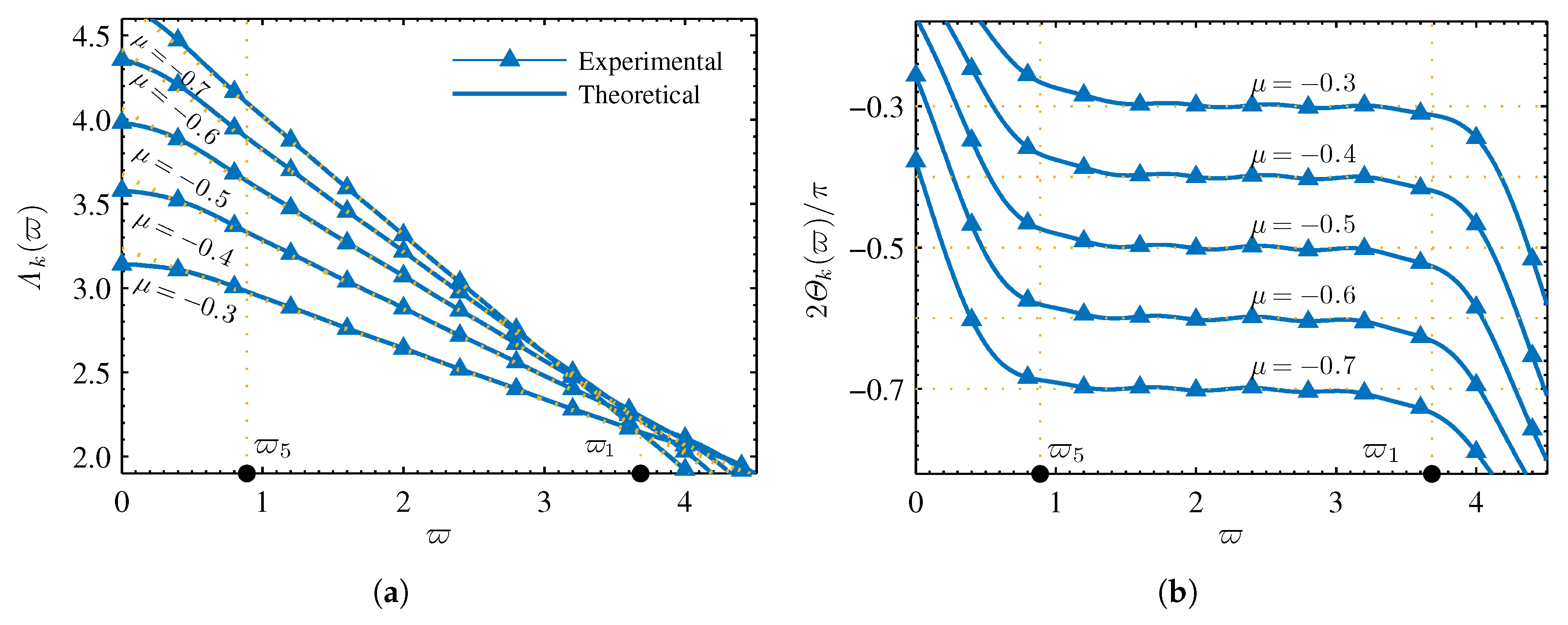
3.2. Frequency Characteristic Analysis

This subsection presents the frequency domain analysis of the approximation performance and variable-order characteristics of the VSFF. The amplitude-frequency characteristic, phase-frequency characteristic, order-frequency characteristic, and F-frequency characteristic function are introduced, and the theoretical and experimental frequency domain characteristic analysis curve of the VSFF is obtained. Subsequently, the frequency domain characteristic curve is analyzed, and the range of the approximation frequency is obtained when the VSFF changes to a different operation order. Lastly, the correlation between the lumped parameter value and the operation order was solved.
The approximation performance and variable-order characteristics of the VSFF were analyzed by using the frequency characteristics. The impedance function of the VSFF was Z ˜ k ( s ) when the operational order changed to μ and the impedance I ˜ ( μ ) ( s ) = F ( μ ) s μ was then approximated. The complex frequency variable, s, was replaced by the exponential frequency variable, ϖ [31]. That is:
s = j 2 π f = j 2 π 10 ϖ .
The amplitude-frequency characteristic functions are:
Λ k ( ϖ ) = lg Z ˜ k j 2 π 10 ϖ Λ ( μ ) ( ϖ ) = lg I ˜ ( μ ) j 2 π 10 ϖ .
The phase-frequency characteristic function is:
θ k ( ϖ ) = arg Z ˜ k j 2 π 10 ϖ θ ( μ ) ( ϖ ) = π 2 μ .
The order-frequency characteristic function [20] is:
O k ( ϖ ) = d Λ k ( ϖ ) d ϖ O ( μ ) ( ϖ ) = d Λ ( μ ) ( ϖ ) d ϖ = μ .
The F-frequency characteristic function [40] is:
Γ k ( ϖ ) = Λ k ( ϖ ) O k ( ϖ ) [ ϖ + lg ( 2 π ) ] Γ ( μ ) ( ϖ ) = lg F ( μ ) .
These functions were used for comparative analysis. Λ k ( ϖ ) , θ k ( ϖ ) , O k ( ϖ ) , and Γ k ( ϖ ) represent the frequency characteristic functions of Z ˜ k ( s ) . Λ ( μ ) ( ϖ ) , θ ( μ ) ( ϖ ) , O ( μ ) ( ϖ ) , and Γ ( μ ) represent the frequency characteristic functions of I ˜ ( μ ) ( s ) . For the circuit configuration shown in Figure 1 and in the case of the parameter values shown in Table 1, when μ = 0.7 , 0.6 , , 0.3 , respectively. r n ( n = 2 , 3 , 4 , 5 ) , c n , r o , and c o were calculated from (13), (14)–(16), respectively. These parameters are substituted into (2). Based on (55)–(58), the theoretical characteristic function curve in the frequency domain was determined, as shown in Figure 4. Figure 4 also shows the simulation experiment results obtained by Multisim 14.
The amplitude-frequency and phase-frequency characteristic function curves, shown in Figure 4a,b, describe the gain and phase characteristics between the voltage and current of the VSFF in the frequency domain, respectively. It can be observed from the amplitude–frequency function curve that the amplitude–frequency characteristic values decreased with increasing frequency. The smaller the operational order, the higher the rate of reduction in the amplitude–frequency characteristic values with increasing frequency. In the low-frequency range, the amplitude—frequency characteristic values decreased with increasing operational order. The phase-frequency and order-frequency characteristic curves, shown in Figure 4b,c, respectively, constitute the mathematical basis to analyze the operational performance (such as the operational order, constant phase, and approximation performance) of the VSFF.
In the case of a fixed operational order, the phase was a fixed value in the approximation frequency range ( 10 ϖ 1 10 ϖ 5 ). When the frequency was less than 10 ϖ 1 , the phase increased with decreasing frequency. When the frequency was greater than 10 ϖ 5 , the phase decreased with increasing frequency. In the case of a fixed frequency, the phase decreased with decreasing operational order. The order-frequency characteristic function represents the operational order of the VSFF from the frequency domain. It can be observed from the order–frequency function curve that the operational order was a fairly constant value in the approximation frequency range ( 10 ϖ 1 10 ϖ 5 ). When the frequency was less than 10 ϖ 1 , the operational order increased with decreasing frequency. When the frequency was greater than 10 ϖ 5 , the operational order decreased with increasing frequency. In the case of a fixed frequency, the operational order decreased with decreasing operational order. The F-frequency characteristic function curve, shown in Figure 4d, represents the lumped parameter value of the VSFF in the frequency domain.
It can be observed from F-frequency function curve that the lumped parameter value was a fairly constant value in the approximation frequency range ( 10 ϖ 1 10 ϖ 5 ). When the frequency was less than 10 ϖ 1 , the lumped parameter value decreased with the decrease in the frequency. When the frequency was greater than 10 ϖ 5 , the lumped parameter value increased with the increase in frequency. In the case of a fixed frequency, the lumped parameter value increased with the decrease in the operational order. The order-frequency and F-frequency characteristic functions visually represent the degree of operational order and the lumped parameter value of the VSFF approximation of the ideal fractor element. It can be observed from the order-frequency and F-frequency characteristic curves, that the VSFF realized the fractional and variable operation orders within a certain frequency range. The highest frequency index value [31],
ϖ 1 = lg [ 1 / ( 2 π R C ) ] ,
and the lowest frequency index value [31],
ϖ k = ϖ 1 ( k 1 ) lg σ , k = 5 ,
were used to realize fractional-order operation.
Therefore, the operating frequency range of the VSFF of the parameters shown in Table 1 was obtained as ( 10 ϖ 1 10 ϖ 5 ), i.e., ( 7.72 Hz 4.82 kHz ). The lumped parameter value, F ( μ ) , was solved within the operating frequency range, as observed from the F-frequency characteristic curve. The correlation between the lumped parameter value, F ( μ ) , and μ was solved by using the least square method to fit the data and to obtain the following equation:
Γ ( μ ) ( μ ) = lg F ( μ ) ( μ ) = 2.2444 μ 2 6.7431 μ + 1.6545 .
The relative error of Γ ( μ ) ( μ ) calculated by (61) within the variation range of μ , was less than 0.05 % .

3.3. Two Equivalent Methods for Calculating Variable-Order Electrical Characteristics

This subsection presents two equivalent methods to calculate the variable-order electrical characteristics to obtain the time-domain theoretical electrical characteristics of the VSFF. One of these methods is derived from circuit theory and is presented in this study. The other variable-order electrical characteristic calculation method is obtained through the Grünwald-Letnikov variable-order fractional calculus.

3.3.1. Variable-Order Electrical Characteristics Obtained through Circuit Theory

For the input voltage signal, u ( t ) , to the VSFF, the current flowing through the VSFF according to Kirchhoff’s current and voltage laws can be represented as follows:
i ( t ) = C β 1 d u ( t ) d t + α 1 k u ( t ) ( α 1 ) R + n = 1 k u ( t ) u n ( t ) α n 1 R ,
where u n ( t ) denotes the voltage across the capacitor, c n n = 1 , 2 , , k , and is described by
β n 1 C d u n ( t ) d t = u ( t ) u n ( t ) α n 1 R , ( n = 1 , 2 , , k ) .
The correlation between α and β in Equations (62) and (63) and the operation order can be obtained from Equation (10). Therefore, the variable-order electrical characteristics of the VSFF can be obtained based on (10), (62) and (63).

3.3.2. Variable-Order Electrical Characteristics Obtained through the Grünwald–Letnikov Definition

The input voltage signal, u ( t ) , to the VSFF and the main spectral range of u ( t ) was within the approximate frequency range of the VSFF. The input current obtained is expressed as follows [13]:
i ( t ) 1 F ( μ ( t ) ) t o D t μ ( t ) u ( t ) ,
where t 0 is the initial time.
Grünwald-Letnikov variable-order fractional calculus was used to define the computation completion (64). It has at least three widely used definitions [15,16,17]. These definitions are based on replacing the constant operational order, μ , with variable operational order, μ ( t ) . The coefficients are then obtained based on different sampling methods. If the coefficient is sampled from the order value at the corresponding time of the coefficient, then [15,16,17]:
i ( t ) = 1 F ( μ ( t ) ) lim h 0 j = 0 t t 0 / h ( 1 ) j h μ ( t j h ) μ ( t j h ) j u ( t j h ) ,
where t < t 0 , u i n ( t ) 0 , and μ ( t j h ) j are binomial coefficients. To complete the numerical calculation of (65), the step size, h, must be sufficiently small; therefore:
i ( t ) 1 F ( μ ( t ) ) j = 0 t t 0 / h ψ j ( μ ( t j h ) ) h μ ( t j h ) u ( t j h ) ,
where ψ j ( μ ( t j h ) ) = ( 1 ) j μ ( t j h ) j represents the polynomial coefficient of the function, ( 1 z ) μ ( t j h ) , which can be directly calculated by using the following recursive formula:
ψ 0 ( μ ( t ) ) = 1 , ψ j ( μ ( t j h ) ) = 1 1 μ ( t j h ) j ψ j 1 ( μ ( t j h ) ) , j = 1 , 2 ,
If μ ( t ) is constant, the calculated result of (66) must be consistent with that defined by the Grünwald-Letnikov fractional calculus of the constant operational order.

3.4. Experimental Verification

In this subsection, the variable-order characteristics of VSFF are experimentally verified. The experimental fields include steady-state, dynamic, and continuous variable order. The steady-state variable-order experiments can be used to prove that a single VSFF can be used as a constant-order fractor of different orders. The dynamic variable-order experiments can prove that the VSFF contains a variable-order process, which can be used in the cases where the operational order requires a jump. For example, in the design of programmable variable-order fractional chaos [18]. The continuous variable-order experiments can be used to demonstrate the capability of VSFF for programmable high-resolution continuous variable-order.
GPS-4303C, TBS1052B, EE16330, TCP312A, and TCPA300, were employed as the power supply, oscilloscope, signal generator, current probe, and current amplifier, respectively. The current probe and amplifier were used to convert the current waveform to a linear voltage signal and to amplify the voltage signal for the oscilloscope test, respectively. The TBS1052B is connected to a PC through a USB interface, which has the Tektronix OpenChoice PC Communications software installed on it to obtain the data that it measured by TBS1052B. Figure 5 depicts the experimental test images.

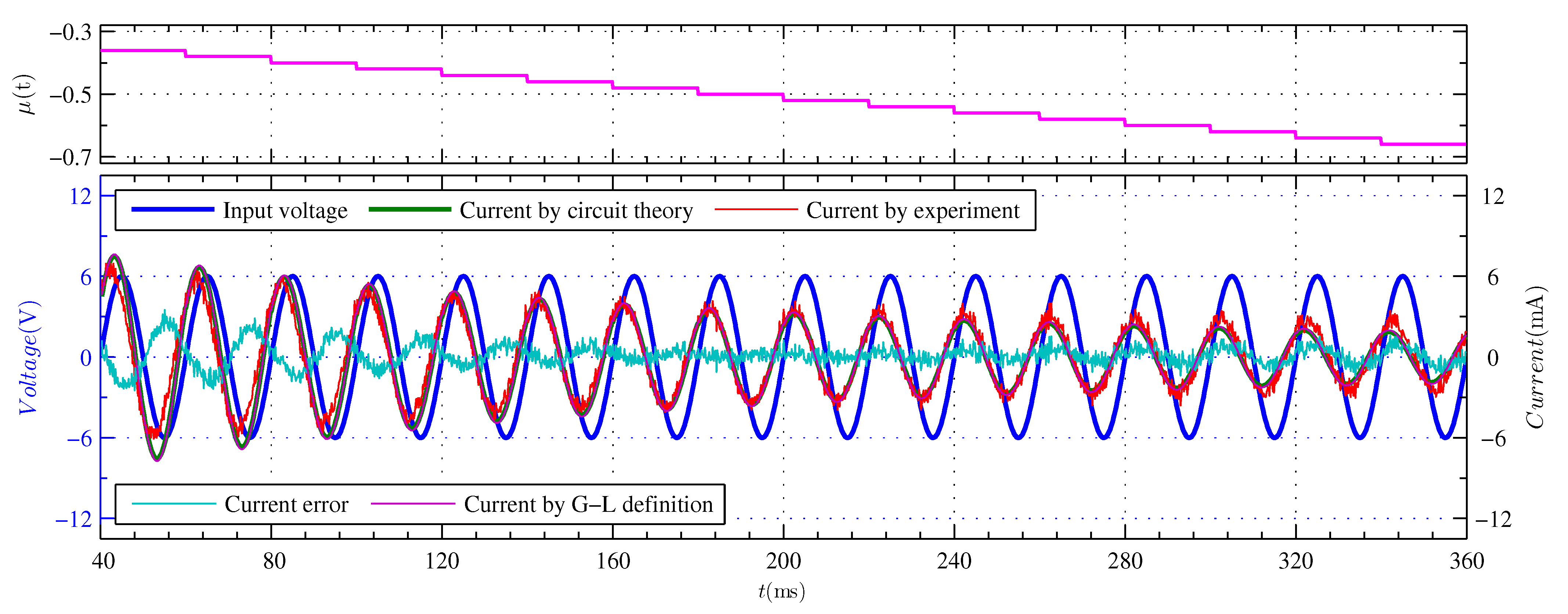
3.4.1. Steady-State Variable-Order Experiment

If the signal generator outputs a sinusoidal voltage signal,
u ( S ) ( t ) = A ( S ) sin 2 π f ( S ) t
to the VSFF, A ( S ) = 10 V , and f ( S ) = 1000 Hz . Then, μ ( t ) is 0.30 , 0.46 , and 0.63 , respectively. The Grünwald-Letnikov definition method is used to calculate the current waveform obtained from (61), (66) and (67), and Figure 6a,c,e presents the corresponding experimental current waveform. If the triangular wave voltage signal, u ( T ) ( t ) , is input into the VSFF, the peak voltage, A ( T ) = 6 V , frequency, f ( T ) = 50 Hz , and μ ( t ) change to 0.32 , 0.48 , and 0.65 , respectively. The Grünwald-Letnikov definition method is used to calculate the current waveform, and Figure 6b,d,f depicts the corresponding experimental current waveform. Furthermore, Figure 6 depicts the current error waveform between the experimental current waveform and the Grünwald-Letnikov definition method is used to calculate the current waveform.
According to the experimental current waveform shown in Figure 6, when the input voltage signals are sinusoidal and triangular, the VSFF can perform steady-state variable-order experiments of different orders. The average values of the current error waveforms shown in Figure 6a–f are 0.4524 mA , 0.1927 mA , 0.2151 mA , 0.0913 mA , 0.1131 mA , and 0.1191 mA , respectively. The standard deviations of the current error waveforms shown in Figure 6a–f are 1.1325 mA , 2.0992 mA , 1.9526 mA , 0.6218 mA , 0.4256 mA , and 0.6348 mA , respectively. When the input amplitude of the voltage waveform is constant, the smaller the operational order, μ ( t ) , the smaller the amplitude of the current waveform. This is consistent with the amplitude-frequency characteristic function curve depicted in Figure 4a. Figure 6a,c,e demonstrates that when μ ( t ) is 0.30 , 0.46 , and 0.63 , the corresponding theoretical phase difference is 27 ° , 41 . 4 ° and 56 . 7 ° , respectively. Figure 6a,c,e also demonstrates that when μ ( t ) is 0.30 , 0.46 , and 0.63 , the corresponding experimental phase difference is 26 . 6 ° , 40 . 5 ° and 53 . 1 ° , respectively. The phase error between the experimental and the theoretical phase is shown in Figure 6a,c,e are 0 . 4 ° , 0 . 9 ° , and 3 . 6 ° , respectively. The phase difference decreases with a decrease in the operational order, μ ( t ) , which is consistent with the phase-frequency characteristic curve presented in Figure b. The experimental results concur well with their theoretical counterparts when the input waveform, amplitude, frequency, and operational order change. The peak value of the input signal was 10 V .

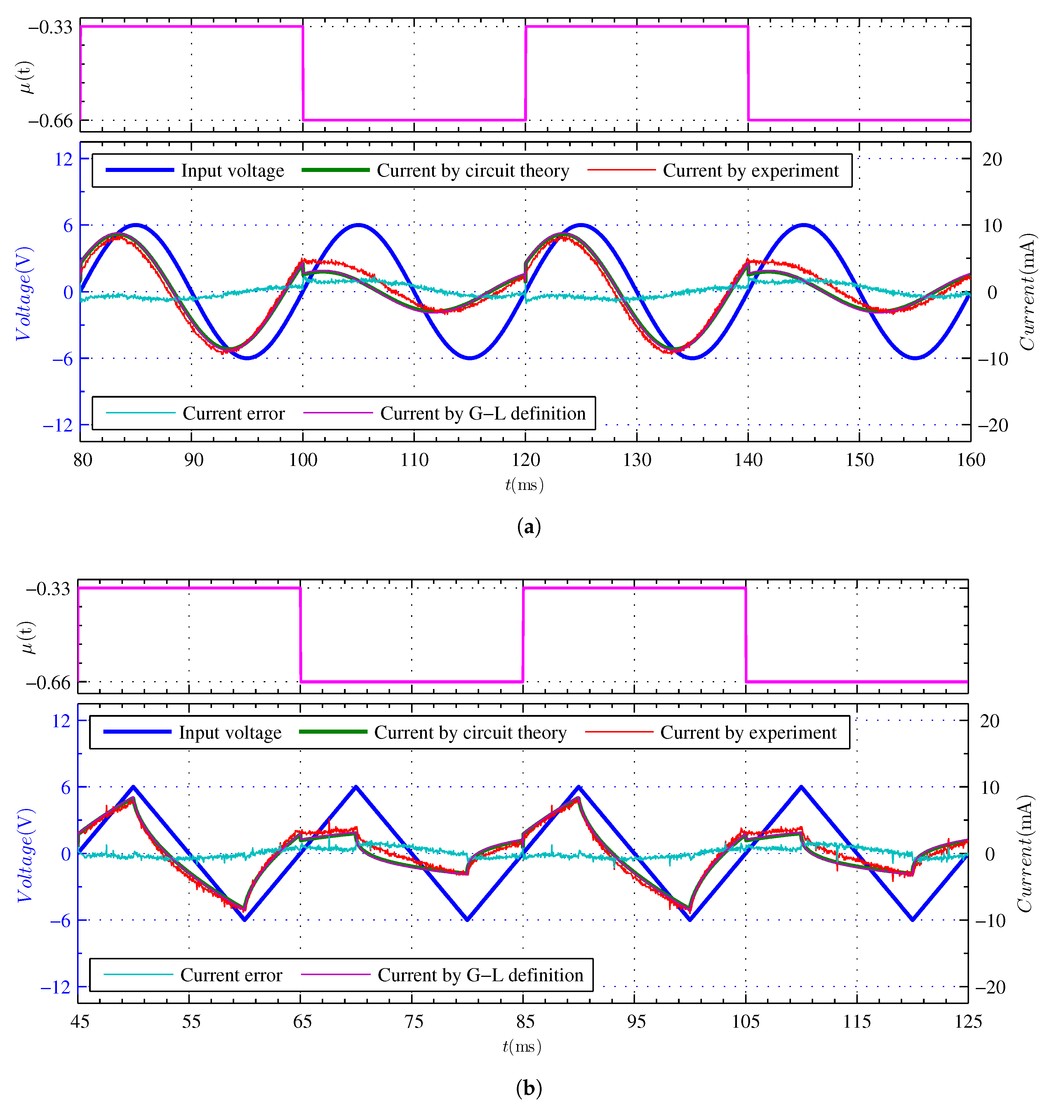
3.4.2. Dynamic Variable-Order Experiment

If the voltage signal, u ( S ) ( t ) , shown in (68) is input to the VSFF and the peak voltage, A ( S ) = 6 V ,
f ( S ) = 50 Hz , μ ( t ) = 0.33 n ˜ f ( S ) t < ( n ˜ + 1 ) 1 f ( S ) 0.66 ( n ˜ + 1 ) 1 f ( S ) t < ( n ˜ + 2 ) 1 f ( S ) , n ˜ = 0 , 1 , 2 ,
Figure 7a presents the circuit theoretical method used to calculate the current waveform obtained from (10), (62) and (63) and the Grünwald-Letnikov definition method used to calculate the current waveform obtained from (61), (66) and (67). Figure 7a presents the corresponding experimental current waveforms. When the triangle wave voltage signal, u ( T ) ( t ) , is input into the VSFF, the peak voltage, A ( T ) = 6 V , frequency, f ( T ) = 50 Hz , and μ ( t ) vary between 0.33 and 0.66 . Figure 7b illustrates the circuit theoretical method used to calculate the current waveform obtained from (10), (62) and (63) and the Grünwald-Letnikov definition method used to calculate the current waveform obtained from (61), (66) and (67). Figure 7b illustrates the corresponding experimental current waveform. Additionally, Figure 7a,b presents the current error waveform between the experimental current waveform and the circuit theoretical method calculated current waveform.
According to the experimental current waveform shown in Figure 7, when the input voltage signals are sinusoidal and triangular, the VSFF can complete dynamic variable-order experiments of different orders. The circuit theoretical method and the Grünwald-Letnikov definition method used to calculate the current waveform overlap perfectly. The accuracy of the variable-order electrical characteristics obtained through circuit theory is verified. The average values of the current error waveforms shown in Figure 7a,b are 0.0517 mA and 0.0723 mA , respectively. The standard deviations of the current error waveforms shown in Figure 7a,b are 0.9938 mA and 0.7473 mA , respectively. At the moment when the operation order jumps, the circuit theoretical method calculated current waveform and the Grünwald-Letnikov definition method calculated current waveform also jump. However, the corresponding experimental waveform jump is not obvious. This is due to parasitic resistance and capacitance parameters in VSFF, test cables, and experimental apparatus, which filter out the high-frequency spectrum during the current waveform jump. According to the experimental current waveform shown in Figure 7, the VSFF completed the change of order within the approximation frequency and operational order ranges.

3.4.3. Continuous Variable-Order Experiment

A continuous variable-order experiment was conducted to fully demonstrate the variable-order capability of the VSFF and to reflect its advantages. If the voltage signal, u ( S ) ( t ) , shown in (68) is input to the VSFF and the peak voltage, A ( S ) = 6 V , the frequency, f ( S ) = 50 Hz , and μ ( t ) change from 0.3 to 0.7 . The variable-order range included the maximum and minimum values of the designed operational order. Figure 8 depicts the circuit theoretical method used to calculate current waveform obtained from (10), (62) and (63) and the Grünwald-Letnikov definition method used to calculate the current waveform obtained from (61), (66) and (67). Figure 8 depicts the corresponding experimental current waveform. Additionally, Figure 8 depicts the current error waveform between the experimental current waveform and the circuit theoretical method used to calculate the current waveform.
The VSFF can perform continuous variable-order experiments based on the experimental current waveform depicted in Figure 8. The circuit theoretical method and the Grünwald-Letnikov definition method used to calculate the current waveform overlap perfectly. The accuracy of the variable-order electrical characteristics obtained through circuit theory is confirmed once again. The larger current error waveforms are partly due to small phase errors. In essence, the current error is not large. The average value and standard deviations of the current error waveforms shown in Figure 8 are 0.1167 mA and 0.7094 mA , respectively. Errors may be caused by many factors such as circuit components, experimental instruments, and frequency domain approximation errors. Errors in circuit components include resistors, capacitors, operational amplifiers, and AD5544. The relative errors of various equivalent parameters of AD5544 caused by resolution have been given in Table 1. Integral non-linearity is also an important factor causing error of AD5544. There is a non-linear relationship between integral non-linearity and digital quantity of AD5544 [39]. The frequency characteristic curves shown in Figure 4 also indicate that there are frequency domain errors that fluctuate with frequency within the approximate frequency range. When the input amplitude of the voltage waveform is constant, μ ( t ) changes from 0.3 to 0.7 , the smaller the amplitude of the current waveform. This is consistent with the amplitude-frequency characteristic function curve shown in Figure 4a. It can also be observed from Figure 8 that when the operation order reduces, the smaller the operation order, the larger the relative error between the experimental current waveform and the theoretical waveform. This is similar to the equivalent relative error variation rule shown in Table 1. It is observed that the equivalent relative error changes from minimum to maximum as the operation order changes from maximum to minimum. It can be observed from Figure 8 that the variable-order scaling fractal-ladder fractor can perform high-resolution continuous variable-order experiments within the range of the operation order. This is because the HRMDAC and other devices can support the requirement of device indicators for continuous operational order varying.
It can also be observed from Figure 8 that when the operation order is large, the amplitude of the experimental current waveform is smaller than that of the theoretical current waveform. When the operation order is small, the amplitude of the experimental current waveform is larger than that of theoretical current waveform. A similar situation is observed in the steady-state variable-order and dynamic variable-order experiments. The error between the experimental waveform and the theoretical waveform, and the operation order exhibit a stable regularity; this type of error is called a systematic error. System errors must be calibrated often in circuit and system design. Therefore, when the results of Figure 6 and Figure 7 are presented, the same systematic error calibration parameters are implemented for the circuit theoretical method, which is used to obtain the current waveform from (10), (62) and (63) and the Grünwald-Letnikov definition method used to obtain the current waveform from (61), (66) and (67). The calibration results used while constructing an application system using VSFF must be more accurate.

4. Discussion

This study implemented the VSFF superior to existing related studies in multiple indicator dimensions. In [13], when the temperature of the solid-state fractor changed within the range of 25∼ 60 ° C , and the operational order changed within a range of only 0.909 0.949 . In [14], when the temperature of the solid-state fractor changed within the range 100∼ 150 ° C , the operational order changed within a range of only 0.77 0.86 . The VSFF implemented in this study used a microcontroller, which is more convenient and efficient than the temperature control method [13,14]. In [19], the operational order switched between 0.2 , 0.5 , and 0.8 . However, the studies conducted on circuit implementation are limited. The variable-order range of the circuit realized in this study was from 0.7 to 0.3 . This significantly exceeds the operational order range of the variable-order fractor [13,14,19] and exhibits high-resolution characteristics. The HMDAC is crucial in the implementation of the VSFF.
In this study, the scaling fractal fractor used in the VSFF exhibited a classic structure. The voltage-controlled resistance and capacitance circuits used the AD633 multiplier as the core in the memristor and memcapacitor emulators [35,36,37]. The resolution and precision requirements of the VSFF for variable circuit parameter adjustment could not be easily satisfied since the accuracy of the AD633 was approximately 2 % . The HMDACs are typically used in the DAC conversion and in multiplier circuits. The HMDAC uses the AD5544, m = 16 bits, and a resolution of Δ K = 1 2 m = 1 65 , 536 . For the emulator, the equivalent minimum relative error δ min x ^ n = 1 65 , 536 x ^ n = c ˜ n , r ˜ n , c o , r o and maximum relative error δ max x ^ n = 6.732 × 10 4 . The programmable resistor–capacitor series circuit and programmable universal electronic component emulators designed using the HMDAC as the core can better meet the requirements of the VSFF parameter adjustment.
In this study, the selection of component parameters is merely an example of the circuit implementation of the VSFF. The technical specifications of VSFF can be adjusted based on the requirement of the actual system. The frequency range of the operations can be increased by increasing the total number of subcircuits. The accuracy can be improved by decreasing the value of the scaling parameter, σ . The VSFF accuracy can also be improved by selecting components with higher precision and resolution. Furthermore, the speed of the variable order can be increased by using faster microcontrollers.
Despite the various advantages presented by the implemented VSFF, it faces certain limitations that must be addressed. Firstly, VSFF is larger and thus requires more space, although it is more flexible and has a wider range of steps when compared to the existing solid-state fractor. Secondly, the VSFF variable-order speed is limited by the control speed of the microcontroller. Lastly, it can be observed from the F-frequency characteristic function curve presented in Figure 4d, that when the operational order of VSFF changes, the lumped parameter value also changes.

5. Conclusions

Variable-order fractor is an important unit or component for realizing variable-order fractional calculus operations. Based on previous studies on scaling fractal fractor with various structures [30,31,32,33,34], the theoretical problem of developing high-resolution emulator circuits to achieve VSFF is a major challenge. This study proposed a VSFF circuit configuration based on the scaling expansion theory [30,31]. A programmable resistor–capacitor series circuit and programmable universal electronic component emulators with HMDAC were designed based on the requirements of the circuit configuration. The experimental content includes steady-state, dynamic and continuous variable-order. The operational order ranged from 0.7 to 0.3 . The operation frequency of the VSFF ranged from 7.72 Hz to 4.82 kHz and the peak value of the input signal was 10 V .
The programmable resistor–capacitor series circuit and the programmable universal electronic component emulators were designed based on the HMDAC. Furthermore, these emulators can be applied to other variable-order fractor circuits, memristor emulators, and memcapacitor emulators. The proposed implementation method can also be used to design the existing scaling fractal-chain [33], fractal-chuan [32], and fractal-lattice [30,31] circuits with variable-order fractor. The VSFF can be used to model natural phenomena and processes of the variable order. The proposed variable-order fractional calculus method that is based on circuit theory can be used as a new time-domain approximation method. More circuit theoretical calculation formulas of variable-order fractional calculus operation can be obtained based on the proposed circuit theoretical calculation method of variable-order fractional calculus operation. The variable-order fractional calculus using circuit theory requires further analysis since it is a novel calculation method.

Author Contributions

Conceptualization, B.Y. and Y.P.; methodology, B.Y. and X.Y.; software, B.Y. and Q.H.; validation, B.Y.; writing—original draft preparation, B.Y.; writing—review and editing, B.Y. and Y.P.; supervision, Y.P.; funding acquisition, Y.P. and B.Y. All authors have read and agreed to the published version of the manuscript.

Funding

This work was supported by the National Natural Science Foundation of China, under Grant 62171303; China South Industries Group Corporation (Chengdu) Fire Control Technology Center Project (non-secret), under Grant HK20-03; National Key Research and Development Program Foundation of China, under Grant 2018YFC0830300; Chengdu Normal University Foundation of China, under Grant CS21ZC02; Classic Undergraduate Course Construction Project in the Sichuan Province of China, under Grant SJYLKC2118; and the Collaborative Education Quality Project of Industry-University Cooperation by the Ministry of Education of China, under Grant 201702119108.

Institutional Review Board Statement

Not applicable.

Informed Consent Statement

Not applicable.

Data Availability Statement

Not applicable.

Conflicts of Interest

The authors declare no conflict of interest.

Abbreviations

The following abbreviations are used in this manuscript:
VSFFVariable-Order Scaling Fractal-Ladder Fractor
HMDACHigh-Resolution Multiplying Digital-to-Analog Converter

References

  1. Sun, H.G.; Yong, Z.; Baleanu, D.; Wen, C.; Chen, Y.Q. A new collection of real world applications of fractional calculus in science and engineering. Commun. Nonlinear. Sci. Numer. Simul. 2018, 64, 213–231. [Google Scholar] [CrossRef]
  2. Baleanu, D.; Agarwal, R.P. Fractional calculus in the sky. Adv. Differ. Equ. 2021, 2021, 117. [Google Scholar] [CrossRef]
  3. Yu, B.; Pu, Y.F.; He, Q.Y. Fractional-Order Dual-Slope Integral Fast Analog-to-Digital Converter with High Sensitivity. J. Circuit. Syst. Comp. 2020, 29, 2050082. [Google Scholar] [CrossRef]
  4. Sun, H.G.; Chang, A.; Zhang, Y.; Chen, W. A review on variable-order fractional differential equations: Mathematical foundations, physical models, and its applications. Fract. Calc. Appl. Anal. 2018, 22, 27–59. [Google Scholar] [CrossRef] [Green Version]
  5. Wu, G.C.; Deng, Z.G.; Baleanu, D.; Zeng, D.Q. New variable-order fractional chaotic systems for fast image encryption. Chaos Interdiscip. J. Nonlinear Sci. 2019, 29, 083103. [Google Scholar] [CrossRef]
  6. Patnaik, S.; Hollkamp, J.P.; Semperlotti, F. Applications of variable-order fractional operators: A review. Proc. Roy. Soc. A-Math. Phy. 2020, 476, 20190498. [Google Scholar] [CrossRef] [Green Version]
  7. Samko, S.G.; Ross, B. Integration and differentiation to a variable fractional order. Integral Transform. Spec. Funct. 1993, 1, 277–300. [Google Scholar] [CrossRef]
  8. Huang, L.L.; Ju, H.P.; Wu, G.C.; Mo, Z.W. Variable–order fractional discrete–time recurrent neural networks. J. Comput. Appl. Math. 2019, 370, 112633. [Google Scholar] [CrossRef]
  9. Wu, F.; Gao, R.B.; Liu, J.; Li, C.B. New fractional variable-order creep model with short memory. Appl. Math. Comput. 2020, 380, 125278. [Google Scholar] [CrossRef]
  10. Gu, X.M.; Sun, H.W.; Zhao, Y.L.; Zheng, X. An implicit difference scheme for time-fractional diffusion equations with a time-invariant type variable order. Appl. Math. Lett. 2021, 120, 107270. [Google Scholar] [CrossRef]
  11. Zheng, X.C.; Wang, H.; Guo, X. Analysis of a Time-Fractional Substantial Diffusion Equation of Variable Order. Fractal Fract. 2022, 6, 114. [Google Scholar] [CrossRef]
  12. Zheng, X.C.; Wang, H. Discretization and Analysis of an Optimal Control of a Variable-Order Time-Fractional Diffusion Equation with Pointwise Constraints. J. Sci. Comput. 2022, 91, 56. [Google Scholar] [CrossRef]
  13. Sheng, H.; Sun, H.G.; Coopmans, C.; Chen, Y.Q.; Bohannan, G.W. A Physical experimental study of variable-order fractional integrator and differentiator. Eur. Phys. J. Spec. Top. 2011, 193, 93–104. [Google Scholar] [CrossRef]
  14. Buscarino, A.; Caponetto, R.; Di Pasquale, G.; Fortuna, L.; Graziani, S.; Pollicino, A. Carbon Black based capacitive Fractional Order Element towards a new electronic device. Int. J. Electron. Commun. 2018, 84, 307–312. [Google Scholar] [CrossRef]
  15. Sierociuk, D.; Malesza, W.; Macias, M. On the Recursive Fractional Variable-Order Derivative: Equivalent Switching Strategy, Duality, and Analog Modeling. Circuits Syst. Signal Process. 2015, 34, 1077–1113. [Google Scholar] [CrossRef] [Green Version]
  16. Sierociuk, D.; Macias, M.; Malesza, W. Analog realization of fractional variable-type and -order iterative operator. Appl. Math. Comput. 2018, 336, 138–147. [Google Scholar] [CrossRef]
  17. Sierociuk, D.; Macias, M.; Malesza, W. Fractional Recursive Variable-Type and Order Operator for a Particular Switching Strategy. Electronics 2020, 9, 855. [Google Scholar] [CrossRef]
  18. Zhou, C.Y.; Li, Z.J.; Xie, F. Coexisting attractors, crisis route to chaos in a novel 4D fractional-order system and variable-order circuit implementation. Eur. Phys. J. Plus. 2019, 134, 73. [Google Scholar] [CrossRef]
  19. Tsirimokou, G.; Psychalinos, C.; Freeborn, T.J.; Elwakil, A.S. Emulation of current excited fractional-order capacitors and inductors using OTA topologies. Microelectron. J. 2016, 55, 70–81. [Google Scholar] [CrossRef]
  20. Yuan, X. Mathematical Principles of Fractance Approximation Circuits; Science Press: Beijing, China, 2015. (In Chinese) [Google Scholar]
  21. Kaplan, T.; Gray, L.J. Effect of disorder on a fractal model for the ac response of a rough interface. Phys. Rev. B 1985, 32, 7360–7366. [Google Scholar] [CrossRef]
  22. Charef, A. Analogue realisation of fractional-order integrator, differentiator and fractional PID controller. IEE Proc.-Control. Theory Appl. 2006, 153, 714–720. [Google Scholar] [CrossRef]
  23. Valsa, J.; Vlach, J. RC models of a constant phase element. Int. J. Circ. Theor. App. 2013, 41, 59–67. [Google Scholar] [CrossRef]
  24. Adhikary, A.; Sen, P.; Sen, S.; Biswas, K. Design and Performance Study of Dynamic Fractors in Any of the Four Quadrants. Circuits Syst. Signal Process. 2016, 35, 1909–1932. [Google Scholar] [CrossRef]
  25. Oustaloup, A.; Levron, F.; Mathieu, B.; Nanot, F.M. Frequency-band complex noninteger differentiator: Characterization and synthesis. IEEE Trans. Circuits Syst. Fundam. Theory Appl. 2002, 47, 25–39. [Google Scholar] [CrossRef]
  26. Morales-Delgado, V.F.; Gómez-Aguilar, J.; Taneco-Hernandez, M.A. Analytical solutions of electrical circuits described by fractional conformable derivatives in Liouville-Caputo sense. Int. J. Electron. Commun. 2017, 134, 108–117. [Google Scholar] [CrossRef]
  27. Roy, D.S. Constant argument immittance realization by a distributed RC network. IEEE Trans. Circuits Syst. 1974, 21, 655–658. [Google Scholar] [CrossRef]
  28. Carlson, G.E.; Halijak, C. Approximation of Fractional Capacitors by a Regular Newton Process. IEEE Trans. Circuit Theory 1964, 11, 210–213. [Google Scholar] [CrossRef]
  29. He, Q.Y.; Yu, B.; Yuan, X. Carlson iterating rational approximation and performance analysis of fractional operator with arbitrary order. Chin. Phys. B 2017, 26, 66–74. [Google Scholar] [CrossRef]
  30. Pu, Y.F.; Yuan, X.; Yu, B. Analog Circuit Implementation of Fractional-Order Memristor: Arbitrary-Order Lattice Scaling Fracmemristor. IEEE Trans. Circuits Syst. I Regul. Pap. 2018, 65, 2903–2916. [Google Scholar] [CrossRef]
  31. Yu, B.; He, Q.; Yuan, X. Scaling fractal-lattice franctance approximation circuits of arbitrary order and irregular lattice type scaling equation. Acta Phys. Sin. 2018, 67, 070202. [Google Scholar]
  32. He, Q.Y.; Pu, Y.F.; Yu, B.; Yuan, X. Scaling Fractal-Chuan Fractance Approximation Circuits of Arbitrary Order. Circuits Syst. Signal Process. 2019, 38, 4933–4958. [Google Scholar] [CrossRef]
  33. He, Q.Y.; Pu, Y.F.; Yu, B.; Yuan, X. A class of fractal-chain fractance approximation circuit. Int. J. Electron. 2020, 107, 1588–1608. [Google Scholar] [CrossRef]
  34. Pu, Y.F.; Yu, B.; Yuan, X. Ladder Scaling Fracmemristor: A Second Emerging Circuit Structureof Fractional-Order Memristor. IEEE Des. Test 2021, 38, 104–111. [Google Scholar] [CrossRef]
  35. Yu, D.S.; Zhao, X.Q.; Sun, T.T.; Iu, H.H.C.; Fernando, T. A Simple Floating Mutator for Emulating Memristor, Memcapacitor, and Meminductor. IEEE Trans. Circuits Syst. II Express Briefs 2020, 67, 1334–1338. [Google Scholar] [CrossRef]
  36. Liang, Y.; Wang, G.; Xia, C.; Lu, Z. Simple modelling of S-type NbOx locally active memristor. Electron. Lett. 2021, 57, 630–632. [Google Scholar] [CrossRef]
  37. Bao, B.C.; Zhu, Y.X.; Ma, J.; Bao, H.; Chen, M. Memristive neuron model with an adapting synapse and its hardware experiments. Sci. China Technol. Sci. 2021, 64, 1107–1117. [Google Scholar] [CrossRef]
  38. Shen, J.; Cong, J.; Chai, Y.; Shang, D.; Shen, S.; Zhai, K.; Tian, Y.; Sun, Y. A non-volatile memory based on nonlinear magnetoelectric effects. Phys. Rev. Appl. 2016, 6, 021001. [Google Scholar] [CrossRef] [Green Version]
  39. ADI. AD5544/AD5554 Data Sheet. [EB/OL]. Available online: https://www.analog.com/media/en/technical-documentation/data-sheets/AD5544_5554.pdf (accessed on 6 July 2022).
  40. Yu, B.; He, Q.; Yuan, X.; Yang, L. Approximation performance analyses and applications of f characteristics in fractance approximation circuit. J. Sichuan Univ. 2018, 55, 301–306. [Google Scholar]
Figure 1. Circuit configuration of VSFF.
Fractalfract 06 00388 g001
Figure 2. Circuit schematic of the n-th programmable resistor–capacitor series circuit emulator ( n = 2 , 3 , , k ).
Fractalfract 06 00388 g002
Figure 3. Circuit schematic of the programmable universal electronic component emulator.
Fractalfract 06 00388 g003
Figure 4. Frequency characteristic curves of VSFF: k = 5 , σ = 5 , R = 330 Ω , and C = 0.1 μ F : (a) amplitude-frequency characteristic; (b) phase-frequency characteristic; (c) order-frequency characteristic; (d) F-frequency characteristic.
Fractalfract 06 00388 g004aFractalfract 06 00388 g004b
Figure 5. VSFF Experiment.
Fractalfract 06 00388 g005
Figure 6. Experimental results of VSFF of steady-state variable-order: (a) sine wave, μ = 0.30 ; (b) triangular wave, μ = 0.32 ; (c) sine wave, μ = 0.46 ; (d) triangular wave, μ = 0.48 ; (e) sine wave, μ = 0.63 ; (f) triangular wave, μ = 0.65 .
Fractalfract 06 00388 g006
Figure 7. Experimental results of VSFF of dynamic variable-order: (a) sine wave; (b) triangular wave.
Fractalfract 06 00388 g007
Figure 8. Experimental results of VSFF of continuous variable-order.
Fractalfract 06 00388 g008
Table 1. Circuit parameter list.
0.7 μ 0.3 , k = 5 , σ = 5
r o , c o 62.3 k Ω r ˜ o 1.41 k Ω , 6.732 × 10 4 δ r ˜ o 1 65 , 536 161 n F c ˜ o 48.0 n F , 1 65 , 536 δ c ˜ o 5.126 × 10 5
R x r o = 1.41 k Ω C x c o = 161 nF
0.9773 K r o 0 0 K c o 0.7023
1-st subcircuit R = 330 Ω C = 0.1 μ F
2-nd subcircuit 1.02 k Ω r ˜ 2 535 Ω , 2.905 × 10 5 δ r ˜ 2 1 65 , 536 162 nF c ˜ 2 309 nF , 2.905 × 10 5 δ c ˜ 2 1 65 , 536
R x ( 2 ) = 535 Ω , C x ( 2 ) = 309 nF
0.4747 K ( 2 ) 0
3-rd subcircuit 3.14 k Ω r ˜ 3 867 Ω , 5.530 × 10 5 δ r 3 ˜ 1 65 , 536 263 nF c ˜ 3 952 nF , 5.530 × 10 5 δ c ˜ 3 1 65 , 536
R x ( 3 ) = 867 Ω , C x ( 3 ) = 952 nF
0.7241 K ( 3 ) 0
4-th subcircuit 9.69 k Ω r ˜ 4 1.40 k Ω , 1.053 × 10 4 δ r ˜ 4 1 65 , 536 426 nF c ˜ 4 2.94 μ F , 1.053 × 10 4 δ c ˜ 4 1 65 , 536
R x ( 4 ) = 1.40 k Ω , C x ( 4 ) = 2.94 μ F
0.8550 K ( 4 ) 0
5-th subcircuit 29.9 k Ω r ˜ 5 2.28 k Ω , 2.004 × 10 4 δ r ˜ 5 1 65 , 536 690 nF c ˜ 5 9.06 μ F , 2.004 × 10 4 δ c ˜ 5 1 65 , 536
R x ( 5 ) = 2.28 k Ω , C x ( 5 ) = 9.06 μ F
0.9239 K ( 5 ) 0
Publisher’s Note: MDPI stays neutral with regard to jurisdictional claims in published maps and institutional affiliations.

