Abstract
With the recently acquired knowledge of the use of a multiphase mixture of precursors under electron beam irradiation (EBI), new possibilities were opened for this technique. In the present work, we obtained quantum dots, nanocrystals, nanoparticles, and grains of PbSe with a sintered appearance using a biphasic mixture of PbSe and PbSeO3 under EBI. High-energy milling was used to obtain the biphasic mixture of precursors, which is composed of agglomerates with sizes ranging from ~400 to ~1700 nm, but nanoparticles were also present. The structural details of the biphasic mixture were studied using X-ray diffraction and the Rietveld method. The driving force of the EBI caused instantaneous physical and chemical changes due to the high internal energy of the biphasic mixture of precursors. The abrupt release of high internal energy, due to localized heating effects during EBI, gave way to the formation of multi-scale PbSe structures. Large particles with a sintered appearance formed near the electron beam impact point and in regions between ~800 nm and ~1400 nm, while well-defined faceted nanostructures were predominantly observed beyond ~1400 nm. The latter tended to be surrounded by {200} facets as the main growth direction. Furthermore, coalescence was anticipated to occur during EBI. It occurred simultaneously with the sublimation mechanism when the particle size was below the critical size of 10 nm. Multi-scale PbSe structures, obtained via EBI, are promising for developing thermoelectric devices due to their crystallinity and nanostructured features.
1. Introduction
As a lead chalcogenide, lead selenide (PbSe) possesses a rock-salt crystal structure and is considered one of the more promising thermoelectric materials. While it has been used in industrial applications involving medium to high temperatures, such as waste heat recovery and power generation [1,2], its availability and lower cost compared to traditional thermoelectric materials make it suitable for large-scale use [3,4,5,6]. It is well known that thermoelectrics benefit from nanoscale particles, which, due to phonon scattering at surfaces, lower thermal conductivity [7,8]. However, there are other modes of phonon scattering that also decrease lattice thermal conductivity and optimize thermoelectric performance [9]. For instance, semi-coherent nanoprecipitates, point defects, and grain boundaries disrupt phonon propagation in numerous frequency ranges while retaining reasonable electrical performance deterioration [10,11,12]. Recently, it has been shown that structuring at multiple scales can greatly reduce lattice thermal conductivity, thus improving the thermoelectric performance of both n-type and p-type PbSe [13,14].
Electron beam irradiation (EBI) is a bottom-up technology that uses active beams to obtain nanostructures [15], which can also produce multi-scale structures instantly [16]. Several physical and chemical processes occur when precursors are irradiated with an electron beam (EB) inside an electron microscope. These processes primarily result from the transfer of kinetic energy and momentum from an EB to atoms, as well as from thermal energy due to beam-induced heating [17,18,19]. Besides, EBI uses a focused beam of high-velocity electrons to initiate chemical [20], structural, and morphological changes in matter [21,22]. In the case of chemical changes, these include chemical bond breaking [23], radiolysis [24], and reduction in oxides [16,23,25], among others. Therefore, due to its versatility, a wide range of materials can be obtained with EBI, including inorganic compounds [16,26], alloys, and polymers [27,28,29,30]. Furthermore, EBI is an ideal technique for developing thermoelectric materials [31,32,33], which is considered an alternative way to nanostructure thermoelectric materials. This technique uses the EB emitted by the gun of a transmission electron microscope as a highly focused and energetic source of electrons for modifying materials at the nanoscale [34,35,36]. Thermoelectric materials nanostructured by EBI are often single-phase pure materials [37,38], inducing highly controlled and selective transformations in the material’s structure [15]. Nevertheless, a multiphase mixture of precursors, including several types of oxides, was recently transformed inside an electron microscope, resulting in the instant formation of multi-scale structures [16].
This work explores the use of EBI to instantly produce various sizes of PbSe structures, with the expectation that structural modifications will improve their thermoelectric properties. To address these concerns, the transition pathway is investigated from a mixture of PbSe and PbSeO3 precursors to multi-scale PbSe structures. The biphasic mixture is produced by high-energy milling (HEM), which results in a product with a high internal energy level [9,39]. The structure, composition, and morphology of the PbSe structures obtained by EBI are analyzed using transmission electron microscopy (TEM) and selected area electron diffraction (SAED). Key concerns regarding the multi-scale PbSe structures growth, the role of the high internal energy level of the biphasic mixture of precursors, and the preferred nucleation sites are also addressed. This makes EBI a powerful tool for developing nanotechnology and materials science applications. In fact, it has not yet been studied exhaustively and remains the focus of researchers. Therefore, it is also believed that this proposal could be used to explore new crystal growth routes, introducing innovative features and methodologies to transform both fundamental understanding and practical applications of semiconductor materials.
2. Materials and Methods
2.1. Materials
A binary mixture of PbO (5 µm) and Se (50 µm) powders was used. These powders were sourced from Sigma-Aldrich, Inc. (St. Louis, MO, USA) with a purity greater than 99.99% by mass.
2.2. Sample Preparation and Milling Treatment
The PbO and Se samples, along with several ZrO2 balls, were sealed together in a cylindrical nylamid polymer with rounded faces to prevent stagnant zones, under c-P-T vial conditions [39]. An overstoichiometric Se addition was considered to achieve a Pb: Se atomic ratio of 1:1, given that the inner volume (60 cm3) contained oxygen in the milling atmosphere (pO2 = 0.2 atm) [40]. The HEM process was carried out using an 8000 Mixer/Mill high-energy ball mill (CertiPrep Inc., Metuchen, NJ, USA), with a fixed ball-to-powder weight ratio of 10:1. It was run for 9 h, after which small amounts of the as-milled reaction products were extracted for further use as precursors.
2.3. Bulk Characterization and Rietveld Refinement
Phase composition and crystallinity of the as-milled sample were determined with a D8 Advance diffractometer (Bruker AXS GmbH, Karlsruhe, Germany). It was carried out in a diffractometer with the Bragg–Brentano θ-θ geometry, Cu-Kα radiation, a Ni 0.5% filter in the secondary beam to remove Cu-kβ, a one-dimensional position-sensitive silicon strip detector, Lynxeye (Bruker AXS GmbH, Karlsruhe, Germany),and a graphite monochromator to discriminate Cu-kα2 from Cu-kα1. The scan was performed at room temperature from 20° to 110° (2θ) in 0.050° steps with a counting time of 0.5 s per step. The amounts of PbSe and PbSeO3 were calculated using Rietveld’s method [40]. The refined parameters included the scale factor, isotropic atomic displacements, atom occupancies, lattice parameters, and anisotropic crystallite size.
2.4. Morphological Characterization
To separate the aggregates into agglomerates and then into clusters or individual nanoparticle arrangements, for high-resolution transmission electron microscopy (HRTEM), TEM, and SAED investigations, the as-milled sample was submerged in 100% ethanol and then ultrasonically deagglomerated. After that, the deagglomerated sample was first placed on a copper grid coated with a holey carbon film for support. Then, a thin layer of carbon was sputtered onto the sample to prevent electron charging. After 9 h of high-energy milling, the morphology, particle size, and atomic structural details of the as-milled sample were examined using a JEOL 2100 transmission electron microscope (JEOL, Tokyo, Japan). An acceleration voltage of 200 kV was used to obtain PbSe structures of different sizes, achieving a point-to-point resolution of 0.27 nm. Based on filament emission, spot size, and the condenser lens aperture, the beam current used to irradiate the sample was estimated to be in the range of a few tens of nanoamperes, 200 keV, with irradiation times of just a few seconds, 3 s, typically sufficient to form multi-scale PbSe structures [16].
3. Results and Discussion
3.1. Bulk Characterization
The Fm-3m space group, as well as the Se (0.0, 0.0, 0.0) and Pb (½, ½, ½) atom locations, were used to represent the symmetry of the PbSe phase. In addition, the monoclinic PbSeO3 phase was modeled using the symmetry represented by the space group P12_1/m1 and the atom locations according to PDF 15-0462. Figure 1 shows a typical Rietveld refinement plot, which demonstrates a high degree of congruence between the calculated and experimental diffraction patterns.
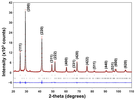
Figure 1.
Typical Rietveld refinement plot of as-milled powders at 9 h. The black continuous line on the upper curve corresponds to the calculated diffraction pattern, while the red dots correspond to the experimental data. The lower blue curve represents the difference between the experimental and the calculated data. The upper grey tick marks correspond to the Bragg positions for PbSe and PbSeO3, respectively, from top to bottom. Note that the Miller indices on the upper diffraction pattern correspond to the PbSe phase.
Based on Rietveld refinement analysis, after 9 h of milling, the sample contained 91.50 (25) wt.% of the PbSe phase and 8.50 (25) wt.% of the PbSeO3 phase, with the numbers in parentheses indicating standard deviations. When they correspond to refined parameters, their values are not given, as these simply estimate the minimal probable errors based on their normal distribution. Consequently, they do not estimate the probable error in the study as a whole [40]. This fact unequivocally establishes that the precursor to be used during EBI is a biphasic mixture constituted by PbSe and PbSeO3.
3.2. TEM Analysis
3.2.1. Before Blasting the Biphasic Mixture with an Electron Beam
Figure 2a shows a typical low-resolution TEM image of the biphasic mixture milled for 9 h. The TEM image shows that the PbSe particles produced initially are agglomerated and form a large aggregate. It consists of submicrometer-sized agglomerates ranging in size from approximately 400 (red dashed line) to ~1700 nm (blue dashed line). Notably, even after ultrasonic dispersion, the aggregates persisted in the sample. This fact shows that particles remain physically joined until greater forces overwhelm them.
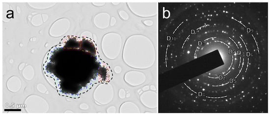
Figure 2.
(a) Typical low-resolution TEM image of a larger micrometer-sized aggregate (black dashed line) in the biphasic mixture—after 9 h of processing time—before blasting due to the EBI; it is constituted by submicrometer-sized agglomerates from ~400 nm (red dashed line) which reach ~1600 nm in size (blue dashed line). (b) Diffraction pattern recorded on the agglomerated particles shown in (a); the white dashed lines reveal the rings associated with the biphasic mixture.
Figure 2b shows the SAED pattern used to determine the crystal geometry, corresponding to Figure 2a. As can be seen, the SAED pattern exhibits rings and spots associated with the phases of the as-milled sample. It reveals a few reflections of the cubic Pb phase, which exhibits a cubic copper structure, see Table 1. Due to the presence of weak diffraction rings in the SAED pattern, it is possible that Pb is present in the form of nanosized particles in very low amounts. Along with that, EDS analyses of the biphasic mixture prior to EBI revealed the punctual presence of Pb within the initial aggregate at a scale below XRD detection limits. It could be associated with a non-stoichiometric phase formed during milling, as has been reported in the literature [39].

Table 1.
The measured dE and theoretical dT values of the interplanar spacings and their corresponding planes for the PbSe and Pb phases.
Figure 3a shows an enlarged image of the edge of a typical aggregate, revealing the presence of PbSe nanoparticles. As shown by the arrows, the size of the roundish-shaped PbSe nanoparticles ranges from 9 to 50 nm. It is worth noting that similar PbSe nanostructures have been obtained through co-precipitation at room temperature [41]. These nanostructures are formed through a process of self-assembly, whereby minute PbSe nanoparticles aggregate and align according to their crystal structures to form larger PbSe nanostructures [42].
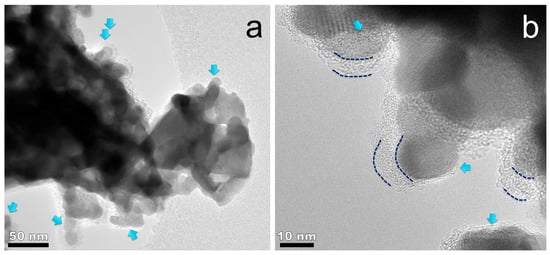
Figure 3.
(a) Typical TEM image of the biphasic mixture milled for 9 h, at the edge of an agglomerate. The arrows indicate the presence of PbSe nanoparticles that are irregular and roundish in shape. (b) An enlarged image of crystalline PbSe nanoparticles coated with a thin layer of amorphous carbon, which was sputtered onto the sample to enhance surface conductivity and prevent charge accumulation under the high-energy electron beam.
As shown by the dashed lines in Figure 3b, the PbSe nanoparticles are roughly spherical and coated with an amorphous carbon layer up to 9 nm thick. The size of such PbSe nanoparticles is typically from ~15 to 25 nm. As indicated by the arrows in Figure 3b, it is worth mentioning that these nanosized particles have a rounded appearance and are crystalline.
3.2.2. After Blasting the Biphasic Mixture with an Electron Beam
Figure 4a illustrates that irradiating the aggregate with EB causes it to break apart, resulting in multi-scale PbSe structures. It is worth keeping in mind that the HEM gives way to metastable structures with high internal energy [9,40]. Then, under EBI, localized heating effects can cause a sudden release of this energy, leading to an explosive disintegration of the agglomerate [16]. Furthermore, EB influences the formation, growth, and coalescence of nanoparticles [37,43], including the reduction in oxides [16,23,25]. Even though the aggregate consists of agglomerates ranging in size from ~400 to 1600 nm (Figure 2a), after EBI, localized heating effects can be created [17,18,19], resulting in a partially melted appearance [37]; see Figure 4a. This is because PbSe’s moderate thermal conductivity makes it easier to trap heat, which can raise its temperature to a point where melting can occur [44,45]. However, due to the presence of PbSe particles smaller than the critical size of 10 nm [46], sublimation can also be expected when the high-energy EB interacts with PbSe atoms during EBI.
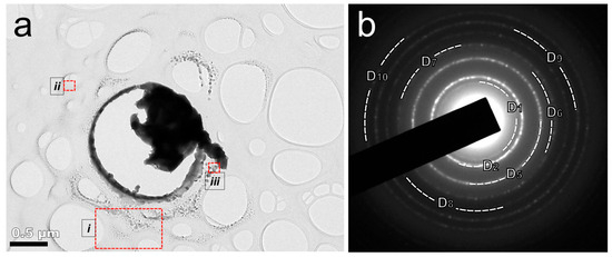
Figure 4.
(a) Typical low-resolution TEM image of the biphasic mixture milled for 9 h, after blasting due to the EBI. (b) Diffraction pattern recorded on the agglomerated particles shown in (a); the dashed lines only reveal rings associated with the PbSe phase, whereas the diffraction rings characteristic of Pb are no longer present, indicating that it has reacted and given way to PbSe.
Figure 4b shows the SAED pattern used to determine the crystal geometry, corresponding to Figure 4a. Well-defined rings and spots are observed, which are associated with the PbSe phase. Therefore, it is important to note that after EBI, the SAED pattern in Figure 4b shows no additional reflections corresponding to the cubic Pb phase, indicating it likely reacts to form PbSe [16,39]. Additionally, the PbSeO3 phase is no longer detected. As documented, EBI of lead oxides results in a phase transformation that decreases the oxygen content until free oxygen phases are obtained [16,47]; such behavior has also been reported by other processes [48].
Figure 5a was obtained from zone i in Figure 4a; the distance from the electron beam impact point ranges from ~800 to ~1500 nm. This zoomed-in image reveals an area with a mixture of partially melted larger particles and minute crystalline particles, respectively. It has been reported that the formation of nanocrystals via EBI processes is influenced by heating effects [17,18,19], which, in turn, are affected by the distance from a heat-conductive substrate [16,37].
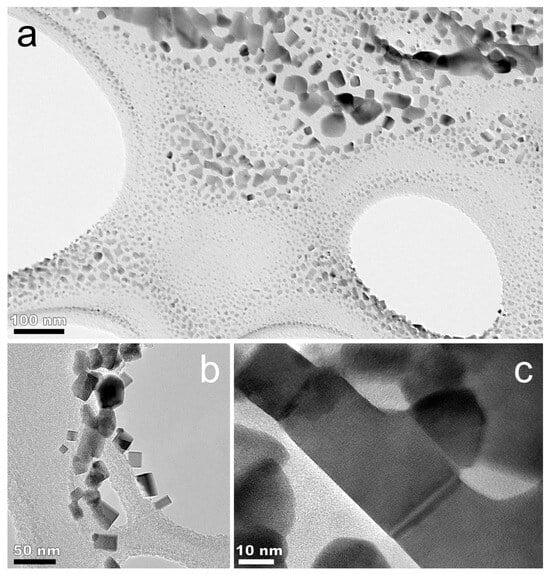
Figure 5b was taken from zone ii in Figure 4a; the distance from the electron beam impact point is nearly 1400 nm. This figure shows the formation of well-defined faceted nanoparticles ranging from 9 to 28 nm after EBI. However, some rounded nanoparticles were also present. As can be seen, this zone does not exhibit partial melting or particles with a sintered appearance. As expected, the perfect cleavage of the cubic PbSe phase causes some PbSe particles to break into cubic nanoparticles, as shown in Figure 5b. As has been documented, this behavior is characteristic of its rock-salt crystal structure, where the arrangement of Pb2+ and Se2− ions creates natural cleavage planes aligned with the cubic lattice axes, which has been consistently demonstrated through crystal growth [49]. Along with that, it is inferred that the PbSe particles are larger near the EB impact point and in regions close to 800 nm because localized heating significantly raises the temperature [17,18,19,50], promoting easier PbSe particle growth. Conversely, in regions further away than 1400 nm, the local temperature due to EBI is expected to decrease [16,17,18,19], and smaller particles are anticipated to be present [37]. Besides, these regions may also experience limited material supply due to lower mobility [50].
Figure 5c was obtained from zone iii in Figure 4a; the distance from the electron beam impact point is nearly 1000 nm. It clearly shows that when the initial aggregate is exposed to EBI, several faceted grains with a sintered appearance are formed [37,43]. When PbSe particles approach each other, within a certain proximity, their surfaces may merge to form larger structures, with well-ordered lattices and a sintered appearance. Besides, secondary recrystallization is also expected to occur due to the growth of larger faceted grains at the expense of smaller ones [17,18,19,50]; see Figure 5a,c. According to published research, enhancing crystallinity increases electrical conductivity and carrier mobility [51]. In this case, the thermal conductivity of the material can be reduced by increasing phonon scattering from nanostructured features [9,52]. Therefore, it is anticipated that the ZT value, which measures overall thermoelectric efficiency, will increase as a result of EBI [14,32,51].
As shown in Figure 6a, the edges of the hole-carbon copper grid are relatively rough, which provides energetically favorable sites for nanoparticle nucleation compared to the smooth areas of the grid [37]. Then, the rapid formation of PbSe nanocrystals during EBI is primarily due to the efficient nucleation process. As seen in Figure 6b–d, this encourages the nucleation and early development of PbSe nanocrystals. This process is facilitated by the roughness of the hole-carbon copper grid, which increases surface energy and provides attachment points for nanocrystal growth [37]. Furthermore, a decrease in PbSe particle size is observed with increasing distance from the EB impact point, particularly beyond 1400 nm [17,18,19,50]; see Figure 6b–d. This phenomenon has also been documented with other types of nanoparticles. As distance increases, the supply of material becomes limited, resulting in smaller particles [16,37,50]. As shown in Figure 6b–d, the {200} faces of PbSe nanoparticles exhibit extensive overlap after EBI. It is worth noting that the distance between nanoparticles influences the process of crystal formation, primarily through its effect on the likelihood of coalescence and atomic and/or oriented attachment [37,53,54].
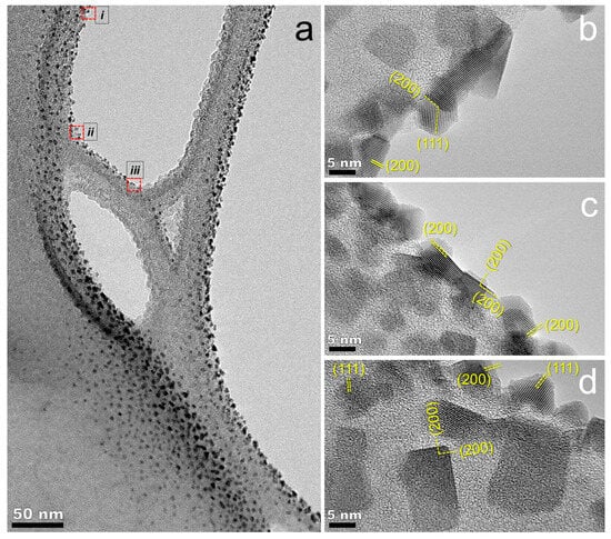
Figure 6.
(a) TEM image of the PbSe nanostructures obtained after blasting due to the EBI. (b–d) Magnified images of the framed zones i, ii, and iii (red dashed lines) in (a). All marked lattice planes on the crystals correspond to the PbSe phase.
According to experimental findings, when PbSe particles come into close contact, atomic flow is expected to occur at the interface, resulting in interpenetration and eventual coalescence into faceted crystal nanostructures [37]; see Figure 7a. For instance, the morphology of these PbSe nanoparticles varies depending on the way in which they interact; see Figure 7c,d. In the case of nanobar interaction, the size of the PbSe nanoparticles was approximately 40 nm. However, the interaction between rounded and nanobar particles resulted in a size of about 39 nm. In contrast, the size was around 17 nm for cubic and rounded particles interacting. More importantly, the surface facets remained intact despite the elongation of the particles, which suggests that a knocking mechanism occurs upon interaction with an EB [52].
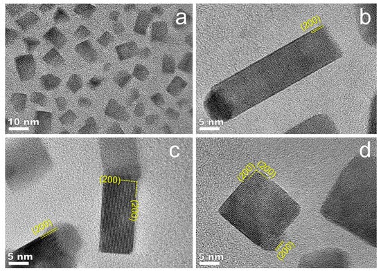
Figure 7.
(a–d) HRTEM image of the PbSe nanostructures obtained after blasting due to the EBI. All marked lattice planes on the crystals correspond to the PbSe phase.
HRTEM images reveal that these PbSe nanostructures are single-crystalline with ordered lattices. It has been documented that atoms organize themselves into thermodynamically stable PbSe crystalline formations with minimal linear and planar defects due to the TEM chamber’s quick cooling and constrained environment [37]. As shown in Figure 7c,d, the {200} facets surrounding PbSe nanostructures demonstrate that this is one of the main growth directions. When nanoparticles are subjected to EBI, their behavior is strongly influenced by the inter-particle distance [55]. Therefore, it is expected that shorter inter-particle distances promote surface diffusion and energy minimization, which drives the process [54,55]. Conversely, larger distances typically impede and/or hinder these processes [56,57,58], resulting in slower growth and less ordered structures.
4. Conclusions
A biphasic mixture of PbSe and PbSeO3 was sensitive to electron beam irradiation when utilizing a transmission electron microscope. By using an accelerating voltage of 200 kV, the experimental findings revealed that, immediately after electron irradiation began, up to 8.50 wt.% of the PbSeO3 phase underwent complete transformation into PbSe. The multi-scale PbSe structures’ distribution points to fragmentation from an explosion caused by the biphasic precursor mixture’s high internal energy and its abrupt release because of localized heating effects during electron beam irradiation. The result was the formation of several types of multi-scale PbSe structures that could be attractive for thermoelectric applications due to their crystallinity and nanostructured features. Additionally, near the electron beam impact point, as well as in regions between ~800 and ~1400 nm, large particles with a sintered appearance were formed; however, in regions beyond 1400 nm, well-defined faceted nanostructures were predominantly obtained. Furthermore, crystallization is expected to occur alongside the coalescence mechanism. Even more, due to the presence of particles smaller than the critical size of 10 nm, sublimation may also occur. The edges of the carbon–copper grid are preferred nucleation sites for PbSe nanocrystal formation, implying that surface roughness increases surface energy and creates attachment sites for PbSe nanocrystal development. Moreover, it is expected that the acquired knowledge of using a biphasic mixture of precursors under electron beam irradiation makes it possible to expand the range of applications of the EBI technique.
Author Contributions
Conceptualization, H.R.-C., M.A.V.-M., N.D. and M.A.; methodology, H.R.-C., M.A.V.-M., N.D., M.A. and J.M.J.-G.; formal analysis, H.R.-C., M.A.V.-M., N.D., M.A. and G.C.-F., investigation, H.R.-C., M.A.V.-M. and J.M.J.-G.; writing—original draft preparation, H.R.-C. and M.A.V.-M.; writing—review and editing, H.R.-C., M.A.V.-M., N.D., M.A., J.M.J.-G. and G.C.-F.; funding acquisition, H.R.-C. and M.A.V.-M. All authors have read and agreed to the published version of the manuscript.
Funding
This research received no external funding.
Data Availability Statement
The original contributions presented in this study are included in the article. Further inquiries can be directed to the corresponding authors.
Acknowledgments
H.R.-C., J.M.J.-G., G.C.-F. and M.A.V.-M. thank the Sistema Nacional de Investigadoras e Investigadores (SNII) for the designation.
Conflicts of Interest
The authors declare no conflicts of interest.
Abbreviations
The following abbreviations are used in this manuscript:
| EB | Electron beam |
| EBI | Electron beam irradiation |
| HEM | High-energy milling |
| HRTEM | High-resolution transmission electron microscopy |
| SAED | Selected area electron diffraction |
| TEM | Transmission electron microscopy |
| XRD | X-ray diffraction |
References
- Luo, Q.; Wang, R.; Lu, K.; Liu, H.; Yuan, G.; Ding, J.; Lei, X.; Min, R.; Zhang, Q.; Huang, L. Boosting the Thermoelectric Properties of N-Type PbSe through the Dual Incorporation of Sb and Al. Mater. Today Commun. 2024, 41, 110718. [Google Scholar] [CrossRef]
- Sousa, V.; Savelli, G.; Lebedev, O.I.; Kovnir, K.; Correia, J.H.; Vieira, E.M.F.; Alpuim, P.; Kolen’ko, Y.V. High Seebeck Coefficient from Screen-Printed Colloidal PbSe Nanocrystals Thin Film. Materials 2022, 15, 8805. [Google Scholar] [CrossRef]
- Hou, Z.-H.; Qian, X.; Cui, Q.-J.; Wang, S.-F.; Zhao, L.-D. Strategies to Advance Thermoelectric Performance of PbSe and PbS Materials. Rare Met. 2024, 43, 4099–4114. [Google Scholar] [CrossRef]
- Sihmar, I.; Pandey, A.; Solet, V.K.; Chaudhary, N.; Goyal, N.; Pandey, S.K. Understanding the Transport Behaviour of PbSe: A Combined Experimental and Computational Study. Next Mater. 2025, 8, 100702. [Google Scholar] [CrossRef]
- Achimovičová, M.; Daneu, N.; Rečnik, A.; Ďurišin, J.; Peter, B.; Fabián, M.; Kováč, J.; Šatka, A. Characterization of Mechanochemically Synthesized Lead Selenide. Chem. Pap. 2009, 63, 562–567. [Google Scholar] [CrossRef]
- Achimovičová, M.; Baláž, P.; Ďurišin, J.; Daneu, N.; Kováč, J.; Šatka, A.; Feldhoff, A.; Gock, E. Mechanochemical Synthesis of Nanocrystalline Lead Selenide: Industrial Approach. Int. J. Mater. Res. 2011, 102, 441–445. [Google Scholar] [CrossRef]
- Piotrowski, M.; Franco, M.; Sousa, V.; Rodrigues, J.; Deepak, F.L.; Kakefuda, Y.; Kawamoto, N.; Baba, T.; Owens-Baird, B.; Alpuim, P.; et al. Probing of Thermal Transport in 50 Nm Thick PbTe Nanocrystal Films by Time-Domain Thermoreflectance. J. Phys. Chem. C 2018, 122, 27127–27134. [Google Scholar] [CrossRef]
- Badr, Y.; Mahmoud, M.A. Size-Dependent Spectroscopic, Optical, and Electrical Properties of PbSe Nanoparticles. Cryst. Res. Technol. 2006, 41, 658–663. [Google Scholar] [CrossRef]
- Rojas-Chávez, H.; Juárez-García, J.M.; Herrera-Rivera, R.; Flores-Rojas, E.; González-Domínguez, J.L.; Cruz-Orea, A.; Cayetano-Castro, N.; Ávila-García, A.; Mondragón-Sánchez, M.L. The High-Energy Milling Process as a Synergistic Approach to Minimize the Thermal Conductivity of PbTe Nanostructures. J. Alloys Compd. 2020, 820, 153167. [Google Scholar] [CrossRef]
- DeCoster, M.E.; Chen, X.; Zhang, K.; Rost, C.M.; Hoglund, E.R.; Howe, J.M.; Beechem, T.E.; Baumgart, H.; Hopkins, P.E. Thermal Conductivity and Phonon Scattering Processes of ALD Grown PbTe–PbSe Thermoelectric Thin Films. Adv. Funct. Mater. 2019, 29, 1904073. [Google Scholar] [CrossRef]
- Deng, Q.; Zhang, F.; Nan, P.; Zhang, Z.; Gan, L.; Chen, Z.; Ge, B.; Dong, H.; Mao, H.; Ang, R. Unique Semi-Coherent Nanostructure Advancing Thermoelectrics of N-Type PbSe. Adv. Funct. Mater. 2024, 34, 2310073. [Google Scholar] [CrossRef]
- Ma, L.; Mei, R.; Zhao, X.; Sun, H. Monte Carlo Simulation of Single-Crystalline PbSe Nanowire Thermal Conductivity Using First-Principle Phonon Properties. Semicond. Sci. Technol. 2017, 32, 095008. [Google Scholar] [CrossRef]
- Liu, S.; Qin, B.; Zhao, L.-D. PbSe Thermoelectrics: Efficient Candidates for Power Generation and Cooling. Adv. Energy Mater. 2025, 15, 2404251. [Google Scholar] [CrossRef]
- Xie, Y.; Deng, Q.; Yang, Y.; Luo, Y.; Ou, W.; Zhao, Z.; Luo, J.; Wu, H.; Ang, R. Pseudo-Nanostructuring and Grain Refinement Enhance the Near-Room-Temperature Thermoelectric Performance in n-Type PbSe. Small 2025, 21, 2408852. [Google Scholar] [CrossRef] [PubMed]
- Tanaka, S.-I. Control and Modification of Nanostructured Materials by Electron Beam Irradiation. Quantum Beam Sci. 2021, 5, 23. [Google Scholar] [CrossRef]
- Rojas-Chávez, H.; Daneu, N.; Valdés-Madrigal, M.A.; Carbajal-Franco, G.; Achimovičová, M.; Juárez-García, J.M. Fast Transformation of PbTe Using a Multiphase Mixture of Precursors: First Insights. Quantum Beam Sci. 2025, 9, 24. [Google Scholar] [CrossRef]
- Watanabe, M.; Someya, T.; Nagahama, Y. Temperature Rise of Specimen Due to Electron Irradiation. J. Phys. D Appl. Phys. 1970, 3, 1461. [Google Scholar] [CrossRef]
- Park, J.; Bae, K.; Kim, T.R.; Perez, C.; Sood, A.; Asheghi, M.; Goodson, K.E.; Park, W. Direct Quantification of Heat Generation Due to Inelastic Scattering of Electrons Using a Nanocalorimeter. Adv. Sci. 2021, 8, 2002876. [Google Scholar] [CrossRef]
- Koenig, C.; da Silva Fanta, A.B.; Jinschek, J.R. Measurement of Electron Beam Induced Sample Heating in SEM Experiments. Ultramicroscopy 2025, 276, 114195. [Google Scholar] [CrossRef]
- Skowron, S.T.; Chamberlain, T.W.; Biskupek, J.; Kaiser, U.; Besley, E.; Khlobystov, A.N. Chemical Reactions of Molecules Promoted and Simultaneously Imaged by the Electron Beam in Transmission Electron Microscopy. Acc. Chem. Res. 2017, 50, 1797–1807. [Google Scholar] [CrossRef]
- Sohn, W.; Kim, M.; Jang, H.W. Atomic-Scale Insights into the 2D Materials from Aberration-Corrected Scanning Transmission Electron Microscopy: Progress and Future. Small Sci. 2024, 4, 2300073. [Google Scholar] [CrossRef]
- Wahlqvist, D.; Mases, M.; Jacobsson, D.; Wiinikka, H.; Ek, M. Nanocarbon Oxidation in the Environmental Transmission Electron Microscope—Disentangling the Role of the Electron Beam. Carbon 2024, 218, 118686. [Google Scholar] [CrossRef]
- Sun, J.; Li, M.; Liu, H.; Guo, L.; Dong, X.; Liang, C. Transmission Electron Microscopy Analysis of Co3O4 Degradation Induced by Electron Irradiation. Micron 2025, 190, 103786. [Google Scholar] [CrossRef]
- Ilett, M.; S’ari, M.; Freeman, H.; Aslam, Z.; Koniuch, N.; Afzali, M.; Cattle, J.; Hooley, R.; Roncal-Herrero, T.; Collins, S.M.; et al. Analysis of Complex, Beam-Sensitive Materials by Transmission Electron Microscopy and Associated Techniques. Philos. Trans. R. Soc. A Math. Phys. Eng. Sci. 2020, 378, 20190601. [Google Scholar] [CrossRef]
- Long, N.J.; Petford-Long, A.K. In-Situ Electron-Beam-Induced Reduction of CuO: A Study of Phase Transformations in Cupric Oxide. Ultramicroscopy 1986, 20, 151–159. [Google Scholar] [CrossRef]
- Mücke, D.; Cooley, I.; Liang, B.; Wang, Z.; Park, S.; Dong, R.; Feng, X.; Qi, H.; Besley, E.; Kaiser, U. Understanding the Electron Beam Resilience of Two-Dimensional Conjugated Metal–Organic Frameworks. Nano Lett. 2024, 24, 3014–3020. [Google Scholar] [CrossRef]
- Atas, M.S. The Relationship between Reinforcement Ratio and E-Beam Irradiation in Y2O3 Reinforced Al6061 Alloys: A Crystallographic Assessment. Nucl. Instrum. Methods Phys. Res. Sect. B Beam Interact. Mater. At. 2024, 548, 165252. [Google Scholar] [CrossRef]
- Ghobashy, M.M.; Sharshir, A.I.; Zaghlool, R.A.; Mohamed, F. Investigating the Impact of Electron Beam Irradiation on Electrical, Magnetic, and Optical Properties of XLPE/Co3O4 Nanocomposites. Sci. Rep. 2024, 14, 4829. [Google Scholar] [CrossRef]
- Abdel Maksoud, M.I.A.; Fahim, R.A.; Kassem, S.M.; Gobara, M.; Awed, A.S. Revealing the Effects of Electron Beam Irradiation on the Structural, Optical, Thermal, and Dielectric Properties of PVC/Ag2WO4 Nanocomposite Films. Opt. Quantum Electron. 2024, 56, 710. [Google Scholar] [CrossRef]
- Lu, J.; Sui, X.; Novoselov, K.S.; Huang, P.; Xu, F.; Sun, L. Electron Beam-Assisted Synthesis and Modification of Electrode/Separator Materials for Lithium-Ion Batteries: Progress and Prospects. Coord. Chem. Rev. 2024, 515, 215954. [Google Scholar] [CrossRef]
- Kim, H.J.; Bae, H.B.; Park, Y.; Choi, S.H. Defect-Engineered Si1−xGex Alloy under Electron Beam Irradiation for Thermoelectrics. RSC Adv. 2012, 2, 12670–12674. [Google Scholar] [CrossRef]
- Rao, S.P.; Sahu, S.; Bano, N.; Shukla, D.K.; Dayal, V. Investigation of Low-Temperature Thermoelectric Properties of Si0.8Ge0.2 Alloy Irradiated by High Energy Electron Beam. Curr. Appl. Phys. 2024, 57, 33–41. [Google Scholar] [CrossRef]
- Oh, I.; Jo, J.; Park, J.; Lee, J.; Shin, H.; Yoo, J.-W. Local Crystallization and Enhanced Thermoelectric Performance of Glassy Carbon Induced by the Electron Beam Irradiation. Curr. Appl. Phys. 2016, 16, 1511–1516. [Google Scholar] [CrossRef]
- He, J.; Li, Z.; Lin, K.; Zhong, R.; Cao, H.; Xie, X.; Pu, G.; Wang, Z.; Wang, Y.; Yin, Q.; et al. High-Energy Electron Beam-Induced Enhanced Thermoelectric Performance and Irradiation Resistance of PEDOT: PSS. ACS Appl. Mater. Interfaces 2025, 17, 32894–32905. [Google Scholar] [CrossRef]
- Jiang, N. Electron Irradiation Effects in Transmission Electron Microscopy: Random Displacements and Collective Migrations. Micron 2023, 171, 103482. [Google Scholar] [CrossRef]
- Speckmann, C.; Mustonen, K.; Propst, D.; Mangler, C.; Kotakoski, J. Electron Irradiation Effects on Monolayer MoS2 at Elevated Temperatures. Phys. Rev. B 2025, 111, 054107. [Google Scholar] [CrossRef]
- Hu, J.; Sun, Y.; Chen, Z. Rapid Fabrication of Nanocrystals through in Situ Electron Beam Irradiation in a Transmission Electron Microscope. J. Phys. Chem. C 2009, 113, 5201–5205. [Google Scholar] [CrossRef]
- Zelenina, I.; Veremchuk, I.; Grin, Y.; Simon, P. In Situ Observation of Electron-Beam-Induced Formation of Nano-Structures in PbTe. Nanomaterials 2021, 11, 163. [Google Scholar] [CrossRef]
- Rojas-Chávez, H. Chemical Models to Map the Transformation from Precursors to Semiconductor Materials at Non-Equilibrium Conditions. RSC Mechanochem. 2025, 2, 723. [Google Scholar] [CrossRef]
- Rojas-Chávez, H.; Reyes-Carmona, F.; Achimovičová, M.; Daneu, N.; Jaramillo-Vigueras, D. PbSe Nanocubes Obtained by High-Energy Milling. J. Nanoparticle Res. 2012, 14, 897. [Google Scholar] [CrossRef]
- Díaz-Torres, E.; Flores-Conde, A.; Ávila-García, A.; Ortega-López, M. Electronic Transport Study of PbSe Pellets Prepared from Self-Assembled 2D-PbSe Nanostructures. Curr. Appl. Phys. 2018, 18, 226–230. [Google Scholar] [CrossRef]
- Díaz-Torres, E.; Ortega-López, M.; Matsumoto, Y.; Santoyo-Salazar, J. Simple Synthesis of PbSe Nanocrystals and Their Self-Assembly into 2D ‘Flakes’ and 1D ‘Ribbons’ Structures. Mater. Res. Bull. 2016, 80, 96–101. [Google Scholar] [CrossRef]
- Li, C.-M.; Robertson, I.M.; Jenkins, M.L.; Hutchison, J.L.; Doole, R.C. In Situ TEM Observation of the Nucleation and Growth of Silver Oxide Nanoparticles. Micron 2005, 36, 9–15. [Google Scholar] [CrossRef] [PubMed]
- Skelton, J.M.; Parker, S.C.; Togo, A.; Tanaka, I.; Walsh, A. Thermal Physics of the Lead Chalcogenides PbS, PbSe, and PbTe from First Principles. Phys. Rev. B 2014, 89, 205203. [Google Scholar] [CrossRef]
- Yokota, T.; Murayama, M.; Howe, J.M. In Situ Transmission-Electron-Microscopy Investigation of Melting in Submicron Al-Si Alloy Particles under Electron-Beam Irradiation. Phys. Rev. Lett. 2003, 91, 265504. [Google Scholar] [CrossRef]
- Cheng, F.; Lian, L.; Li, L.; Rao, J.; Li, C.; Qi, T.; Cheng, Y.; Zhang, Z.; Zhang, J.; Wang, J.; et al. Sublimation and Related Thermal Stability of PbSe Nanocrystals with Effective Size Control Evidenced by in Situ Transmission Electron Microscopy. Nano Energy 2020, 75, 104816. [Google Scholar] [CrossRef]
- Pan, Z.W.; Dai, Z.R.; Wang, Z.L. Lead Oxide Nanobelts and Phase Transformation Induced by Electron Beam Irradiation. Appl. Phys. Lett. 2002, 80, 309–311. [Google Scholar] [CrossRef]
- Rojas-Chávez, H.; Miralrio, A.; Cruz-Martínez, H.; Martínez-Espinosa, J.A.; Carbajal-Franco, G.; Juárez-García, J.M. Identifying the Mechanistic Insights into PbSeO3 Decomposition, during Milling, to Give Way to PbSe: An Experimental and Theoretical Approach. Comput. Mater. Sci. 2022, 206, 111291. [Google Scholar] [CrossRef]
- Lin, Z.; Yin, A.; Mao, J.; Xia, Y.; Kempf, N.; He, Q.; Wang, Y.; Chen, C.-Y.; Zhang, Y.; Ozolins, V.; et al. Scalable Solution-Phase Epitaxial Growth of Symmetry-Mismatched Heterostructures on Two-Dimensional Crystal Soft Template. Sci. Adv. 2016, 2, e1600993. [Google Scholar] [CrossRef]
- Ru, Q. Nanocrystals Synthesized by Electron-Beam Induced Fragmentation of Vacancy-Containing Metals Microspheres. Appl. Phys. Lett. 1997, 71, 1792–1794. [Google Scholar] [CrossRef]
- Beniwal, P.S.; Batra, Y. Irradiation-Induced Modifications in the Thermoelectric Performance of Tellurides: A Comprehensive Review. Solid State Sci. 2025, 168, 108030. [Google Scholar] [CrossRef]
- Gayner, C.; Sharma, R.; Malik, I.; Kumar, M.; Singh, S.; Kumar, K.; Tahalyani, J.; Srivastava, T.; Kar, K.K.; Yokoi, H.; et al. Enhanced Thermoelectric Performance of PbSe-Graphene Nanocomposite Manufactured with Acoustic Cavitation Induced Defects. Nano Energy 2022, 94, 106943. [Google Scholar] [CrossRef]
- Rojas-Chávez, H.; Miralrio, A.; Cruz-Martínez, H.; Carbajal-Franco, G.; Valdés-Madrigal, M.A. Oriented-Attachment- and Defect-Dependent PbTe Quantum Dots Growth: Shape Transformations Supported by Experimental Insights and DFT Calculations. Inorg. Chem. 2021, 60, 7196–7206. [Google Scholar] [CrossRef]
- Zulfiqar, A.; Honkanen, M.; Nonappa; Vippola, M. In Situ TEM Imaging Reveals the Dynamic Interplay Between Attraction, Repulsion and Sequential Attraction-Repulsion in Gold Nanoparticles. Small 2024, 20, 2406943. [Google Scholar] [CrossRef]
- Yin, P.; Hu, S.; Qian, K.; Wei, Z.; Zhang, L.-L.; Lin, Y.; Huang, W.; Xiong, H.; Li, W.-X.; Liang, H.-W. Quantification of Critical Particle Distance for Mitigating Catalyst Sintering. Nat. Commun. 2021, 12, 4865. [Google Scholar] [CrossRef]
- Stamatopoulou, P.E.; Zhao, W.; Rodríguez Echarri, Á.; Mortensen, N.A.; Busch, K.; Tserkezis, C.; Wolff, C. Electron Beams Traversing Spherical Nanoparticles: Analytic and Numerical Treatment. Phys. Rev. Res. 2024, 6, 013239. [Google Scholar] [CrossRef]
- Toth, M.; Lobo, C.; Friedli, V.; Szkudlarek, A.; Utke, I. Continuum Models of Focused Electron Beam Induced Processing. Beilstein J. Nanotechnol. 2015, 6, 1518–1540. [Google Scholar] [CrossRef] [PubMed]
- Cheng, L.; Zhu, X.; Su, J. Coalescence between Au Nanoparticles as Induced by Nanocurvature Effect and Electron Beam Athermal Activation Effect. Nanoscale 2018, 10, 7978–7983. [Google Scholar] [CrossRef] [PubMed]
Disclaimer/Publisher’s Note: The statements, opinions and data contained in all publications are solely those of the individual author(s) and contributor(s) and not of MDPI and/or the editor(s). MDPI and/or the editor(s) disclaim responsibility for any injury to people or property resulting from any ideas, methods, instructions or products referred to in the content. |
© 2025 by the authors. Licensee MDPI, Basel, Switzerland. This article is an open access article distributed under the terms and conditions of the Creative Commons Attribution (CC BY) license (https://creativecommons.org/licenses/by/4.0/).