1. Introduction
Thermoelectric (TE) materials have emerged as a pivotal solution for sustainable energy conversion, enabling the direct transformation of waste heat into electricity and addressing global energy challenges and environmental concerns [
1,
2,
3,
4]. The efficiency of TE materials is quantified by the dimensionless figure of merit
ZT =
S2σT/
κ, where
S,
σ, T, and
κ =
κe +
κl denote the Seebeck coefficient, electrical conductivity, temperature, and total thermal conductivity (the sum of electrical
κe and lattice thermal conductivity
κl at a given temperature T.), respectively [
5,
6,
7,
8]. Despite significant advancements in traditional TE materials—such as Bi-based alloys and Pb-based compounds—their energy conversion efficiency remains constrained by the inherent trade-off among
S,
σ, and
κ [
9,
10,
11,
12]. Layered materials like Bi
2Se
3 [
13,
14,
15,
16] and Bi
2Te
3 [
17] show promise, with room-temperature
ZT values exceeding 1.0 achieved through strategies like doping, nanostructuring, and strain engineering. However, realizing high-performance TE devices necessitates further optimization of transport properties, particularly within two-dimensional (2D) systems that offer unique opportunities for tailored properties [
18,
19,
20,
21].
The pursuit of high-performance thermoelectric materials has spurred researchers to investigate the unique properties of 2D materials [
22,
23,
24]. Owing to their low-dimensional structure, which induces interface phonon scattering and phonon confinement effects, 2D materials exhibit intrinsically low thermal conductivity (
κ), with their values being significantly lower than those of their bulk counterparts [
23]. Leveraging this inherent advantage, scientists have extensively studied diverse 2D materials for thermoelectric applications. Both transition metal dichalcogenides (TMDs), such as MoS
2, WS
2, MoSe
2, and HfS
2 [
18,
25,
26], and group IVA-VA compounds, like SnSe, SnS, and GeSe, have demonstrated remarkable thermoelectric performance in numerous studies [
27,
28,
29]. TMDs have attracted significant interest due to their stable structures, semiconducting nature, and high charge carrier mobility. Specific TMDs, including WS
2, WSe
2, HfS
2, and SnSe
2, have shown notably high thermoelectric performance. Furthermore, a novel class of 2D materials, XY
2 (X = Si, Ge, Sn, Pb; Y = Se, Te), has been theoretically predicted to possess high thermoelectric efficiency [
23,
24,
30]. Beyond single-layer 2D materials, researchers’ interest in van der Waals (vdW) heterostructures composed of various TMDs has surged owing to the superior physical and chemical properties compared to their constituent monolayers [
23]. Strong interfacial phonon scattering within these heterostructures results in intrinsically low thermal conductivity, enabling significantly enhanced thermoelectric performance. Among single-layer TMDs, MoS
2 has been widely explored, both theoretically and experimentally, as a promising thermoelectric material, with its monolayer counterpart demonstrating considerable potential [
31,
32,
33,
34].
Recent advances in optimizing monolayer MoS
2 (ML-MoS
2) for thermoelectric applications reveal multiple effective strategies: Vanadium doping induces p-type behavior and enhances
ZT to 0.24 at 860 K by increasing carrier concentration while reducing
κl through point defects [
35]. Sulfur vacancies suppress lattice thermal conductivity by 50–80% via phonon localization, though electron scattering limits n-type performance [
36]. Biaxial 6% tensile strain boosts the
ZT of structural analog ZrS
2 to 2.4 at 300 K through band convergence and phonon softening enhancement [
37], while uniaxial strain along the zig-zag direction enhances
ZT of MoS
2 by 150% via simultaneous mobility improvement and
κl reduction [
23]. Layer engineering shows that a two-layer WSe
2 achieves
ZT > 1 [
38], and MoS
2/MoSe
2 aperiodic superlattices reach
ZT = 1.38 at 500 K through phonon localization [
39]. Copper doping can reduce the Seebeck coefficient of MoS
2 film but effectively reduce the band gap and improve the carrier concentration, thus improving the electrical performance and power factor [
34]. Niobium doping can enhance the electrical and thermoelectric properties of MoS
2, which not only facilitates the development of thermoelectric devices and offers a route to bipolar thermoelectric devices by decoupling the Seebeck coefficient from electrical conductivity, achieving a power factor of approximately 370 μW·m
−1·K
−2 at room temperature, but also extends to other TMDs like WS
2 and WSe, showing great potential in applications such as on-chip cooling, thermal sensors, bipolar junctions, and photovoltaics. [
40]. Collectively, these studies demonstrate that synergistic control of electronic and phononic properties—via doping, defects, strain, heterostructuring—can decouple the traditional
S-
σ-
κ trade-off. Critically, while strain and doping individually enhance performance, synergistic application involving combining them with electric fields remains largely unexplored for maximizing
ZT in ML-MoS
2 [
40,
41].
While dopant introduction remains one of the most investigated methods for enhancing thermoelectric performance, it inevitably induces permanent changes to the material and can sometimes lead to secondary phase formation [
40,
42]. In contrast, strain engineering, owing to its simplicity and reversibility, presents a compelling alternative for modulating electronic and thermoelectric properties. For monolayer, few-layer, and bulk MoS
2, strain application has proven to be an effective method for tuning and enhancing thermoelectric performance [
18,
23,
43,
44]. Significant experimental efforts have focused on achieving various in-plane tensile or compressive strains on monolayer and few-layer MoS
2, typically by growing films on stretchable polymers or lattice-mismatched substrates [
23,
30]. Concurrently, researchers have increasingly explored the influence of electric fields, finding that electric fields can induce substantial band structure changes crucial for device operation [
19,
45] and affect surface electrical interactions. Applying electric fields can also alter optoelectronic properties, electron transport, molecular motion, and chemical reactions [
46,
47,
48]. Given the high sensitivity of thermoelectric material parameters to electrical characteristics, electric field-induced performance optimization emerges as a highly intriguing approach.
According to the above research, it can be concluded that various modeling methods have been employed in the study of thermoelectric properties of MoS2 and its heterostructures. First-principles density functional theory (DFT) is widely used to investigate electronic structures, mechanical properties, and phonon transport, as seen in studies on strain effects in monolayer MoS2, the structural properties of MoS2/MoSe2 superlattices, and twisted bilayer MoS2. Semi-classical Boltzmann transport theory (BTE) complements DFT to calculate thermoelectric parameters like Seebeck coefficient and power factor, applied in analyzing bulk and monolayer MoS2. A tight-binding (TB) model combined with non-equilibrium Green’s function (N-EGF) is utilized to explore lateral heterostructures under external fields. Molecular dynamics (MD) simulations assess thermal stability, as in monolayer MoS2 studies. For material preparation and modification, approaches include doping (e.g., Sb, Cu, Ni, and V doping to tune band structures and microstructures), defect engineering (sulfur vacancies, grain boundaries), interlayer modification (cesium intercalation), and strain engineering (uniaxial/biaxial strain, twist angle adjustment) to optimize thermoelectric performance. These methods collectively advance the understanding and improvement of MoS2-based thermoelectric materials.
In this work, leveraging first-principles calculations combined with Boltzmann transport theory, we systematically investigate the influence of uniaxial strain (a or b-axis), temperature variation, and out-of-plane (c-axis) electric fields on the structure, electrical properties, and thermoelectric performance of ML-MoS2. Notably, the application of c-axis electric fields for modulating MoS2 thermoelectric performance has received scant attention in the existing literature. We demonstrate that stress, temperature, and electric fields all significantly impact the Seebeck coefficient, electrical conductivity, and thermal conductivity (both electronic κe and lattice κl), thereby optimizing the thermoelectric figure of merit ZT within specific carrier concentration ranges. Crucially, we identify that suppression of lattice thermal conductivity (κl) is the most dominant factor for enhancing ZT. While stresses in the range of −2% to +2% induce only modest changes in κl, this property exhibits high sensitivity to increasing temperature and, most pronouncedly, to the applied electric field. The external electric field proves exceptionally effective, capable of reducing κl down to single-digit values (W·m−1·K−1), leading to a significant enhancement in ZT. Consequently, we assert that investigating the optimization of thermoelectric performance via electric fields—especially in monolayers or thin films—is a highly effective strategy. Furthermore, synergistic control through stress, temperature, and electric fields holds great promise for maximizing the thermoelectric performance of MoS2 and even more thermoelectric materials.
3. Results and Discussion
The crystalline structure of monolayer ML-MoS
2 exhibits unique physical and chemical properties attributed to its layered architecture. In its fundamental single-layer configuration, each MoS
2 layer comprises a molybdenum atomic sheet sandwiched between two sulfur atomic layers, forming an S-Mo-S tri-atomic layer. This single-layer structure maintains geometric stability through strong in-plane covalent bonding: the Mo atom resides at the center of a hexagonal lattice, equidistantly surrounded by S atoms in a planar triangular prismatic arrangement. This configuration ensures robust covalent interactions between Mo and adjacent S atoms, while interlayer interactions are dominated by weak vdW forces. This structural feature grants MoS
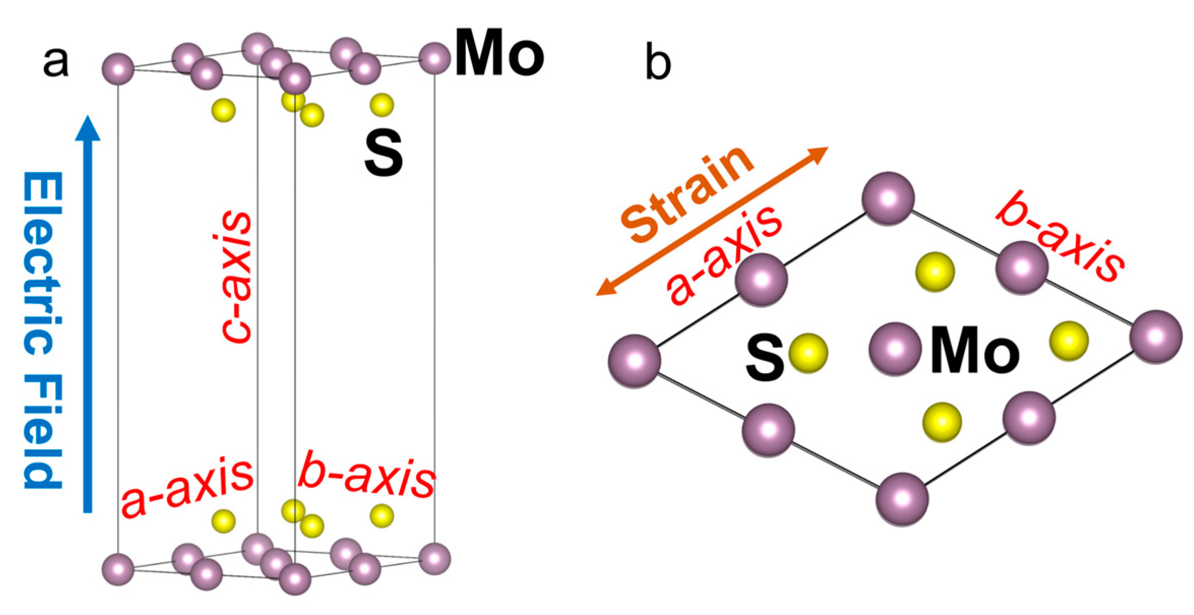
2 exceptional “exfoliability,” enabling facile mechanical exfoliation into single layers. As depicted in
Figure 1, the ML-MoS
2 crystal structure features van der Waals stacking along the c-axis and hexagonal symmetry in the ab-plane. The blue and orange arrows in this figure denote the applied electric field (c-axis direction) and in-plane uniaxial stress (a-axis direction), respectively. The optimized lattice parameters—lattice constant a = 3.166 Å and interlayer spacing c = 17.428 Å—align well with prior computational results [
49,
50].
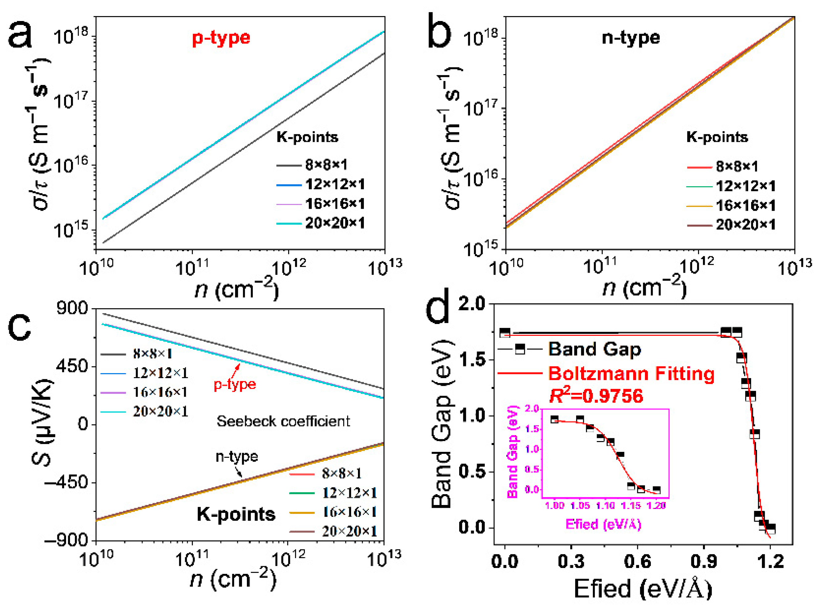
Figure 2a–c show the ratio of electrical conductivity
σ to relaxation time
τ (
σ/
τ) and Seebeck coefficients (
S) for n- and p-type MoS
2 obtained by employing 8 × 8 × 1, 12 × 12 × 1, 16 × 16 × 1, and 20 × 20 × 1 k-point samplings. It is demonstrated that the 12 × 12 × 1 Monkhorst–Pack k-mesh can provide converged results. Thus, this k-point sampling approach was adopted in this study to evaluate the transport coefficients.
Figure 2d presents the band gap (
Eg) results for MoS
2 under different c-axis applied electric fields ranging from 0.00 eV/Å to 1.20 eV/Å. Notably, the
Eg remains almost unchanged when the electric field is lower than 1.05 eV/Å. When the electric field exceeds 1.05 eV/Å, the
Eg begins to decrease rapidly—specifically, the
Eg is only 0.10 eV at 1.05 eV/Å, and it approaches zero with further increases in the electric field. As a core parameter affecting the performance of thermoelectric materials, the
Eg directly influences carrier transport characteristics, energy conversion efficiency, and the applicable temperature range of the material.
To investigate the effect of strain on the thermoelectric properties of ML-MoS
2, in-plane uniaxial strain was applied by modifying the lattice parameter
a. The magnitude of strain is defined by
, where
a0 = 3.166 Å represents the optimized lattice parameter of strain-free ML-MoS
2. Considering experimental feasibility and structural stability, a uniaxial strain ranging from −2% to 2% was applied to ML-MoS
2. Calculations of the total energy under different strains revealed negligible total energy differences between strained and unstrained states (ranging from −22.33953 eV to −22.41935 eV for −2% to 2% strain), indicating that strained states can exist in a highly stable form. The effects of strain on the electronic structure of MoS
2 were further explored.
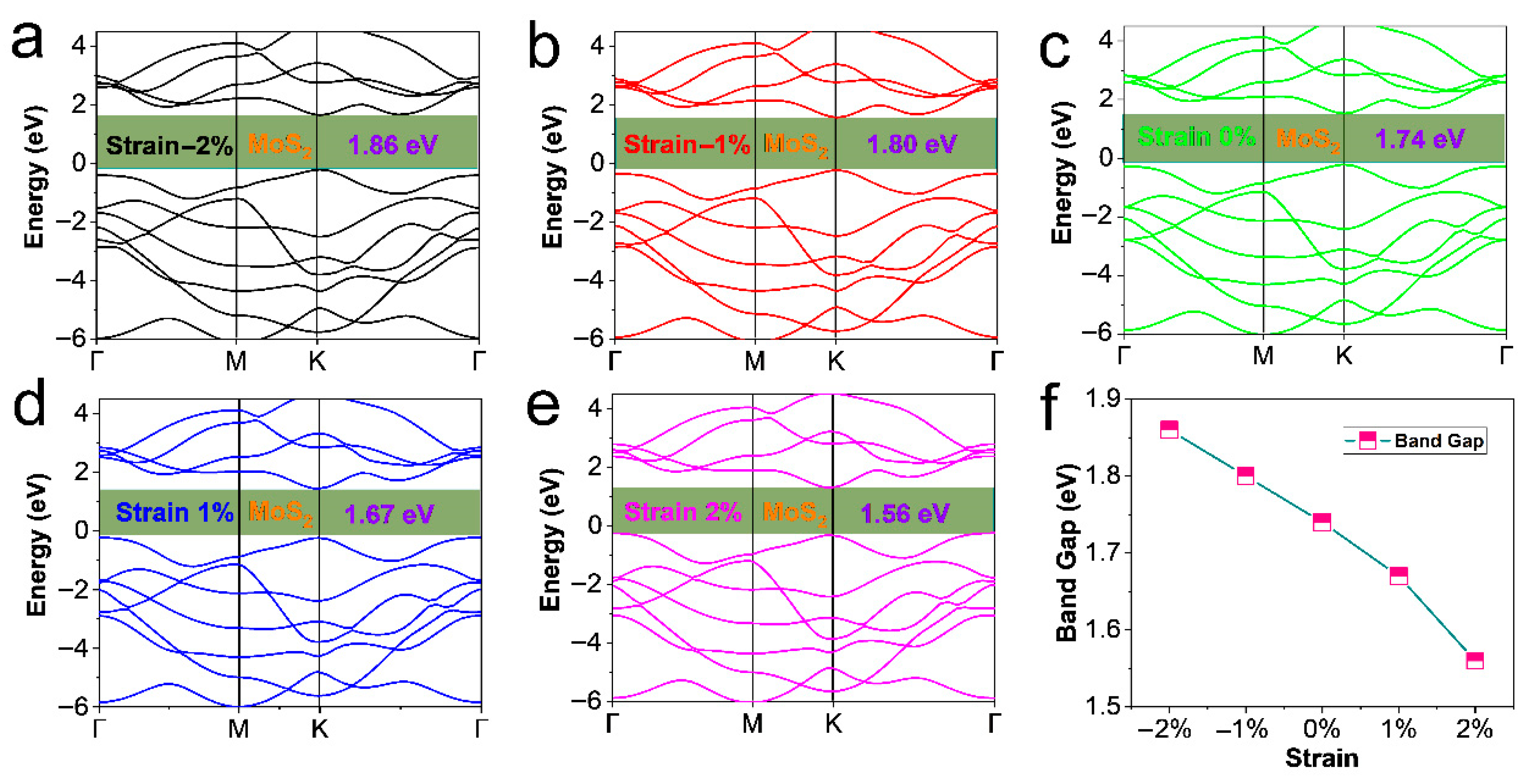
Figure 3 presents the calculated band structures of MoS
2 under varying stresses along the a-axis using the GGA-PBE functional.
Figure 3a–e corresponds to −2%, −1%, 0%, 1%, and 2% strains, respectively, while
Figure 3f illustrates the trend of
Eg width as a function of stress. For strain-free MoS
2, the
Eg exhibits indirect character with a value of 1.74 eV (
Figure 3c), in good agreement with previous calculations of 1.736 eV [
23] and 1.77 eV [
51]. Notably, the
Eg gradually increases as the stress transitions from compression to tension, and the Fermi level decreases from −1.054 eV to −1.203 eV.
The band gap of ML-MoS
2 decreases monotonically with tensile strain (from 1.86 eV at −2% to 1.56 eV at 2%,
Figure 3f), following the physical trend of strain-induced lattice expansion reducing orbital overlap. A smaller
Eg favors higher
σ (by lowering carrier activation energy) but often suppresses
S (as narrow gaps reduce the energy selectivity of carriers). Conversely, compressive strain widens
Eg, which can enhance
S via stronger energy filtering but sacrifices
σ. This trade-off is a classic challenge in TE optimization, and strain provides a knob to tune
Eg and balance
S vs.
σ. For instance, the optimal strain may exist where
Eg is narrowed just enough to boost
σ without severely degrading
S [
40,
43,
52].
To further elucidate the influence of strain on the electronic structure of ML-MoS
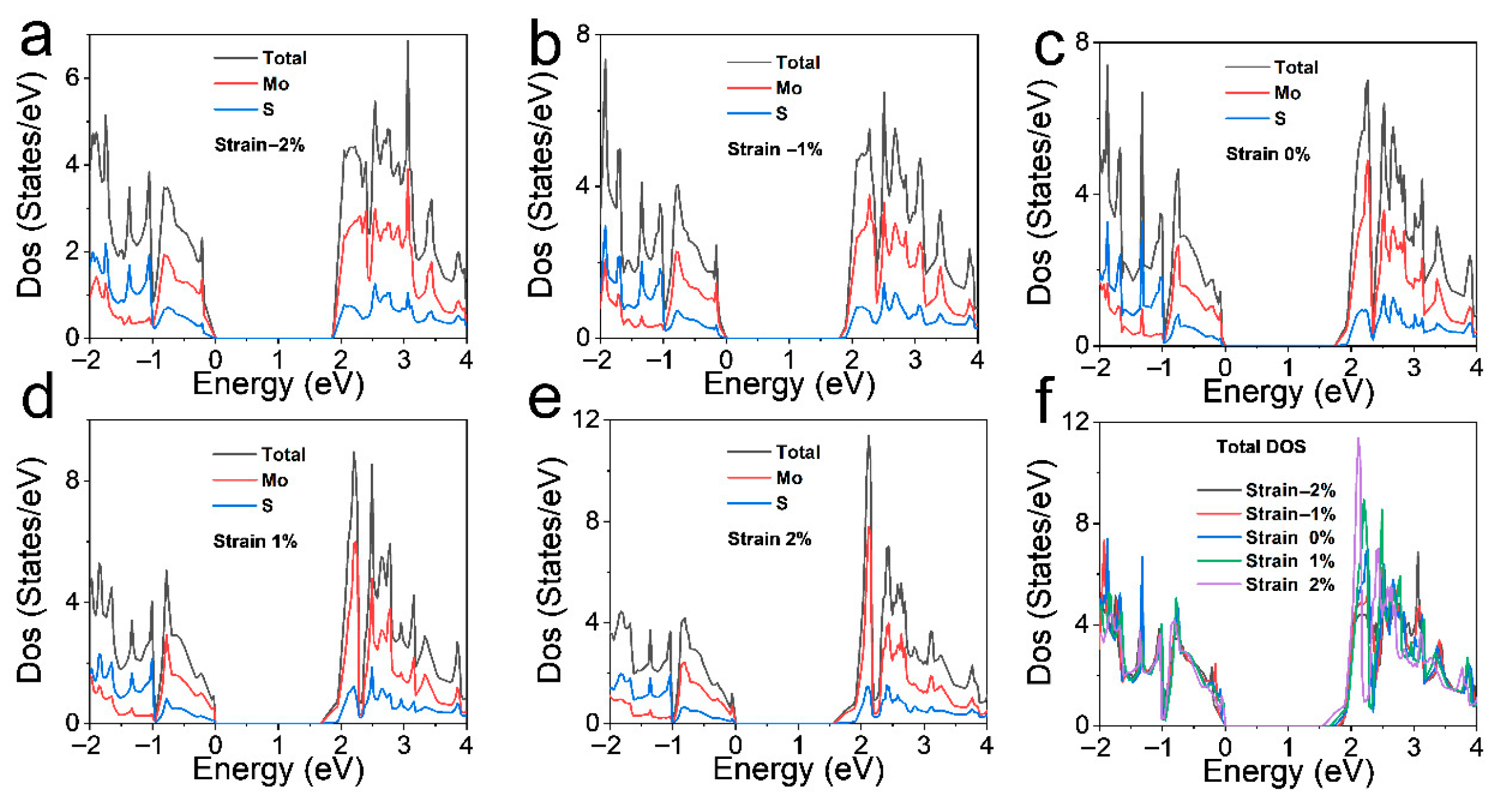
2, the density of states (DOS) was calculated under different uniaxial strains along the a-axis, and the results are presented in
Figure 4. The DOS reflects the number of available electronic states at a given energy level, which is crucial for understanding the thermoelectric transport properties, as the Seebeck coefficient and electrical conductivity are closely related to the DOS near the Fermi level. As shown in
Figure 4a–e, the total DOS and the partial DOS of Mo and S exhibit distinct variations with strain. For the strain-free case (
Figure 4c), the total DOS shows characteristic peaks that are in good agreement with the electronic structure features of MoS
2 reported in previous studies. Under compressive strain (
Figure 4a,b), the DOS near the Fermi level is modified. The peaks corresponding to Mo and S orbitals are shifted, and their intensities are altered, indicating changes in the orbital hybridization and electronic interactions.
When tensile strain is applied (
Figure 4d,e), the DOS distribution is significantly changed. The overall shape of the DOS curves is broadened compared to the strain-free state, and the peaks are either flattened or shifted to higher energies. This implies that tensile strain affects the electronic state distribution by changing the lattice structure and interatomic bonding. Specifically, the partial DOS of Mo shows a more pronounced contribution under 1% and 2% strain (
Figure 4d,e) compared to the strain-free state, suggesting that strain enhances the participation of Mo orbitals in this energy region. The total DOS under different strains is comprehensively compared in
Figure 4f. It is evident that strain can effectively modulate the DOS of MoS
2 across the entire energy range. The variations in DOS with strain directly impact the thermoelectric properties, as the density and distribution of electronic states determine the carrier concentration and mobility. These DOS changes induced by strain provide a fundamental basis for tuning the thermoelectric performance of ML-MoS
2, and further investigations into the transport properties based on these DOS characteristics will be crucial for optimizing the thermoelectric figure of merit
ZT.
Figure 5 systematically illustrates the strain-tuned Seebeck coefficient (
S), relaxation time-scaled electrical conductivity (
σ/τ), and thermoelectric power factor, PF/
τ (
S2σ/τ), of MoS
2, distinguishing between p-type and n-type conduction behaviors at 300 K. For p-type MoS
2 (
Figure 5a–c), the
S in
Figure 5a exhibits a decreasing trend with increasing carrier concentration (
n), which is consistent with the classic thermoelectric transport theory, where
S is inversely related to carrier density in degenerate semiconductors. Under tensile strain,
S is enhanced at the same carrier concentration compared to the strain-free case, indicating that strain can modulate the energy filtering effect of carriers. This is in line with the DOS analysis in
Figure 4, where strain alters the electronic state distribution near the Fermi level, thus affecting the
S. The electrical conductivity-related parameter
σ/τ (
Figure 5b) for p-type MoS
2 shows an increasing trend with
n, as higher carrier concentration generally leads to more efficient charge transport. Tensile strain slightly boosts
σ/τ at low carrier concentrations, which can be attributed to the strain-induced modification of the band structure that reduces carrier scattering. The PF/
τ shown in
Figure 5c integrates the contributions of
S and
σ, and its peak value shifts with strain. Tensile strain broadens the range of carrier concentrations at which the PF/
τ remains elevated. The maximum PF/
τ value of 7 × 10
10 W·m
−1·K
−2·s
−1 occurs at 1% tensile strain and a carrier concentration of
n ≈ 3 × 10
13 cm
−2, indicating significant potential for optimizing the thermoelectric performance of p-type MoS
2 under tailored strain conditions.
For n-type MoS
2 (
Figure 5d–f), the
S in
Figure 5d displays negative values, characteristic of electron-dominated conduction. Similarly to the p-type, the value of
S decreases with increasing
n, but the magnitude and strain dependence differ. Compressive strain significantly enhances the absolute value of S for n-type MoS
2 at moderate carrier concentrations, which is crucial for improving the thermoelectric voltage generation capability. The
σ/τ for n-type MoS
2 (
Figure 5e) increases monotonically with
n, and strain introduces subtle changes in the slope of the curves, implying that strain affects the carrier mobility-related scattering mechanisms. The PF/
τ for n-type MoS
2 (
Figure 5f) shows a complex strain-dependent behavior. Strain creates a higher peak of PF/
τ at a certain carrier concentration, indicating that strain can effectively optimize the power factor of n-type MoS
2. This phenomenon can be explained by the combined effects of strain on the band structure (as observed in the band structure and DOS analyses) and carrier transport. By comparing the p-type and n-type results, it is evident that strain can be used as a versatile tool to tailor the thermoelectric properties of MoS
2 for both electron- and hole-dominated conduction, which is of great significance for the design of high-performance thermoelectric devices based on 2D MoS
2. The strain-induced variations in thermoelectric parameters observed here are also supported by theoretical models of 2D thermoelectric materials in the previously referenced literature, further validating the importance of strain engineering in enhancing the thermoelectric performance.
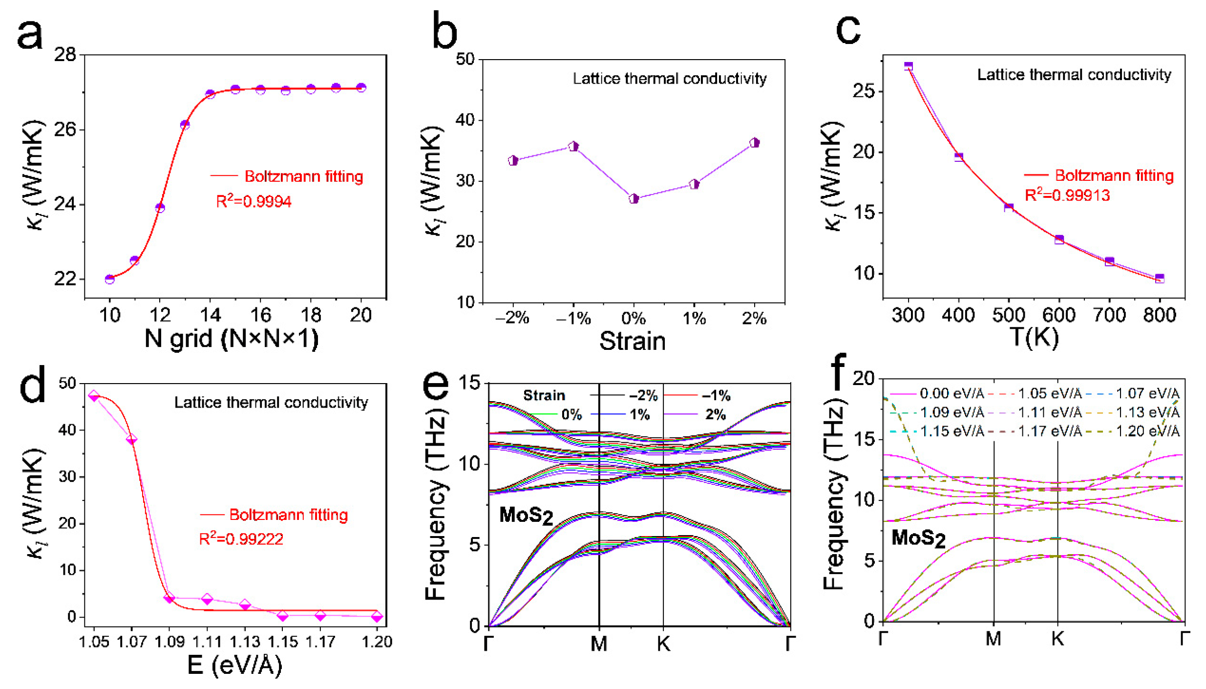
To comprehensively analyze the thermal transport behavior of ML-MoS
2 under strain and electric field engineering,
Figure 6 presents a systematic investigation of lattice thermal conductivity (
κl) and phonon spectra. In
Figure 6a, the mesh convergence test for pristine MoS
2 confirms the reliability of the calculated
κl values, with a high Boltzmann fitting coefficient indicating the convergence of the simulation. Research indicates that, for the ML-MoS
2 material, the total thermal conductivity,
κ =
κe +
κl, is primarily dominated by
κl, as the electronic contribution is at least two orders of magnitude lower than the lattice contribution [
23]. Therefore, effectively reducing
κl becomes one of the crucial factors for enhancing the
ZT value of MoS
2 [
23,
30,
53].
Figure 6b illustrates the suppression of
κl under a-axis tensile strain. As the strain increases from −2% to 2%, the changes in
κl are not significant. This indicates that the degree of strain regulation of
κl is limited. The phonon spectra under strain (
Figure 6e) show distinct shifts and broadening of the phonon modes, which directly correlate with the
κl variations in
Figure 6b. Regarding the temperature-dependent behavior,
Figure 6c depicts the reduction in
κl with increasing temperature. The Boltzmann fitting accurately captures the trend of
κl decreasing as temperature rises, which is a typical feature of phonon-dominated thermal transport in semiconductors. At higher temperatures, enhanced phonon–phonon scattering leads to a more significant reduction in
κl.
Figure 6d shows the electric field-tuned
κl modulation along the c-axis. As the electric field varies from 1.05 eV/Å to 1.20 eV/Å,
κl exhibits a clear dependence on the electric field strength. The Boltzmann fitting indicates a strong correlation between the electric field and
κl modulation. This electric field-induced
κl change is related to the modification of electron–phonon interactions, as the electric field can alter the electronic structure and thus influence the phonon transport. Phonon dispersion under different electric fields (
Figure 6f) shows no unstable modes, confirming dynamic stability. The absence of significant softening implies practical viability for device applications.
As mentioned earlier, the figure of merit for thermoelectric materials is
ZT =
S2σT/
κ, so it is necessary to calculate the relaxation time
τ, combined with
S,
σ/
τ, and PF/
τ in
Figure 5, in order to calculate the
ZT value of the material. However, it is difficult to determine
τ because it depends on both carrier concentration and temperature. By utilizing deformation potential (DP) theory, in combination with the effective mass approximation,
τ can be calculated as [
54,
55]
where
and T are the Planck constant and temperature, respectively. The effective mass
m* of the carrier is defined as
, and the elastic constant can be given by
, where
E1 is the total energy under a-axis uniaxial strain. After calculation, the relaxation times
τ of p-type and n-type MoS
2 materials are 36.57 fs and 489.72 fs, respectively, which is similar to other related calculation results [
24,
30].
Based on the above results, the strain-modulated
ZT at 300 K of MoS
2 can be obtained, as shown in
Figure 7 for both p-type (
Figure 7a) and n-type (
Figure 7b) behavior as a function of carrier concentration n. For p-type MoS
2,
ZT first rises and then falls with increasing n, forming a peak that shifts and changes in magnitude under different strains. Tensile strain (1%) can enhance the maximum
ZT value and adjust the optimal carrier concentration for peak
ZT. For n-type MoS
2, a similar trend exists, but the strain-induced changes in
ZT show distinct characteristics compared to p-type, with compressive strain having a significant impact on boosting
ZT and expanding the range of high
ZT carrier concentrations. These variations in
ZT under strain are closely related to the strain-induced modifications of the electronic structure and thermoelectric transport properties shown above. The
ZT behavior of MoS
2 under strain reflects the comprehensive effect of strain on the thermoelectric parameters. For p-type behavior, the optimal
ZT under certain tensile strains corresponds to the balanced improvement in the power factor, which benefits from the strain-tuned band structure that optimizes carrier transport and energy filtering. For n-type behavior, the enhanced
ZT under compressive strain can be attributed to the increased absolute Seebeck coefficient. Overall, strain engineering proves to be an effective means to modulate the
ZT of MoS
2, providing insights for optimizing the thermoelectric performance of 2D MoS
2 materials.
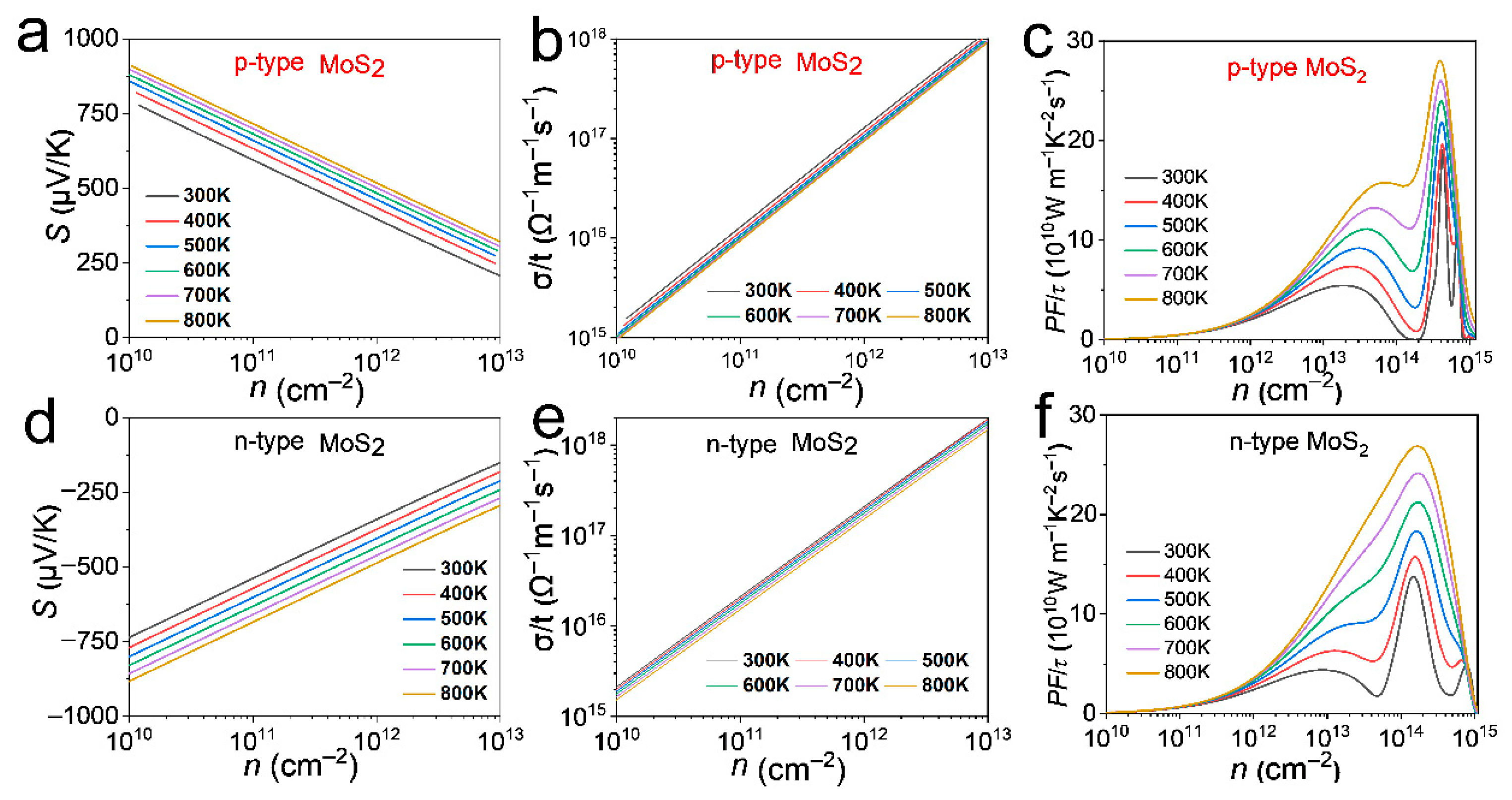
Figure 8 elucidates the temperature-dependent thermoelectric behaviors of MoS
2 across 300 K–800 K, distinguishing p-type and n-type conduction. For p-type MoS
2, the Seebeck coefficient
S in
Figure 8a exhibits a decreasing trend with rising carrier concentration
n at all temperatures, while
S generally increases with elevated temperatures. This aligns with the enhanced thermal excitation at higher temperatures, which strengthens the energy filtering effect of carriers, consistent with the carrier transport mechanisms in 2D thermoelectric materials. The
σ/τ (
Figure 8b) increases with n across all temperatures and shows a slight upward trend with rising temperatures, indicating that higher temperatures facilitate charge transport. As a result, the PF/
τ (
Figure 8c) grows with temperature; its peak emerges at
n ≈ 4 × 10
14 cm
−2, and the maximum value at 800 K reaches approximately 28 × 10
10 W·m
−1·K
−2·s
−1, highlighting the critical role of temperature in boosting p-type thermoelectric performance. For n-type MoS
2, analogous trends are observed. The
S in
Figure 8d and
σ/τ in
Figure 8e follow variation patterns similar to those of p-type MoS
2:
S decreases with n yet increases with temperature, and
σ/τ rises with both n and temperature. The PF/
τ (
Figure 8f) also escalates with temperature, with its peak at
n ≈ 2 × 10
14 cm
−2; at 800 K, the maximum PF/
τ is approximately 27 × 10
10 W·m
−1·K
−2·s
−1. These results corroborate the universal mechanism that elevated temperatures enhance carrier-related transport properties, thereby optimizing the power factor for both conduction types.
Figure 9 presents the temperature- and carrier-concentration-dependent
ZT for both p-type (
Figure 9a) and n-type (
Figure 9b) MoS
2 across the temperature range of 300 K to 800 K. For p-type MoS
2,
ZT shows a remarkable enhancement with increasing temperature. At lower temperatures,
ZT values are relatively small and only exhibit a distinct peak at a specific carrier concentration (
n). As the temperature rises, the peak of
ZT becomes more prominent, and the range of n corresponding to high
ZT values broadens. For instance, at 800 K, the peak
ZT value is significantly higher compared to that at 300 K, and this peak occurs at a carrier concentration of approximately
n ≈ 5 × 10
13 cm
−2, and the maximum
ZT reaches about 0.18. This trend is consistent with the temperature-dependent improvements in the power factor (PF/
τ) observed in
Figure 8c, where higher temperatures facilitate greater thermoelectric performance by enhancing the synergy between
S and
σ/τ. For n-type MoS
2, a similar temperature-induced
ZT enhancement is observed (
Figure 9b). With an increase in temperature from 300 K to 800 K, the
ZT peaks become more pronounced, and the optimal carrier concentration for maximum
ZT shifts. At 800 K, the peak
ZT reaches a relatively high value, occurring at around
n ≈ 3 × 10
13 cm
−2, and the maximum
ZT reaches nearly 2.9. This behavior can be attributed to the combined effects of temperature on the thermoelectric parameters of n-type MoS
2, as analyzed in
Figure 8d–f, where elevated temperatures improve
S,
σ/τ, and, ultimately, the power factor, demonstrating that temperature is a crucial factor in optimizing the
ZT of MoS
2.
Figure 10 investigates the impact of c-axis electric fields on the band structures of MoS
2, spanning electric field strengths from 0.00 eV/Å to 1.20 eV/Å. As the electric field applied along the c-axis increases, distinct modifications in the band structure of MoS
2 are observed. In the absence of an electric field (
Figure 10a), MoS
2 exhibits an indirect band gap with a value of 1.74 eV, consistent with the intrinsic electronic structure characteristics reported in previous studies. As the electric field strength rises (
Figure 10b–i), the band gap of MoS
2 gradually decreases. For example, at an electric field of 1.15 eV/Å (
Figure 10g), the band gap is significantly reduced to approximately 0.10 eV. This electric field-induced band gap modulation is closely related to the quantum confinement and Stark effects, which alter the energy levels and orbital interactions within the MoS
2 lattice. Such changes in the band structure under electric fields play a crucial role in tuning the electronic and thermoelectric properties of MoS
2 as the band gap directly influences carrier excitation, mobility, and the overall thermoelectric transport mechanisms. These findings complement the strain engineering studies presented earlier, highlighting that electric field manipulation along the c-axis is another effective approach to tailor the electronic structure of MoS
2 for optimized thermoelectric performance, in line with the multi-parameter engineering strategies explored in the context of 2D thermoelectric materials.
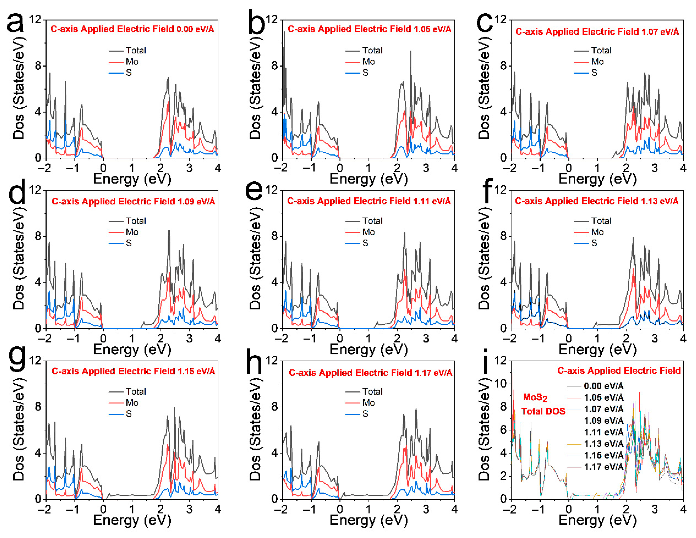
Figure 11 explores the density of states (DOS) of MoS
2 under varying c-axis electric fields, complementing the band structure analysis in
Figure 10. As the electric field applied along the c-axis changes (from 0.00 eV/Å in
Figure 11a to 1.17 eV/Å in
Figure 11h), distinct alterations in the total DOS and the partial DOS of Mo and S are observed. In the absence of an electric field (
Figure 11a), the DOS features characteristic peaks that align with the intrinsic electronic structure of MoS
2. As the electric field strength increases, the positions and intensities of these DOS peaks are modified, indicating changes in the orbital hybridization and electronic interactions within the MoS
2 lattice. For instance, under a higher electric field, the DOS near the Fermi level shows a more pronounced redistribution, which can be attributed to the electric field-induced band structure modifications (as seen in
Figure 10). The total DOS comparison in
Figure 11i further illustrates the systematic variation in DOS with electric field strength, highlighting the ability of electric fields to tune the electronic states of MoS
2. These changes in DOS are crucial for understanding the electric field-mediated thermoelectric properties of MoS
2, as the DOS directly influences carrier concentration, mobility, and the resulting thermoelectric transport phenomena. Consistent with the research on 2D material engineering in the provided references, the electric field-induced DOS modulation in MoS
2 offers a viable pathway to optimize its thermoelectric performance by tailoring the electronic structure at the atomic level. The total and partial DOS (Mo/S orbitals) show field dependent peak shifts and broadening. In the low-field region (≤1.05 eV/Å), Mo and S DOS peaks are well separated near the Fermi level, indicating weak band hybridization and a relatively large band gap, with the total DOS retaining the intrinsic structure. In the mid-field region (1.07–1.15 eV/Å), their DOS peaks start to overlap near the Fermi level, enhancing the DOS at the Fermi level and potentially boosting the Seebeck coefficient via energy filtering. Above ~1.13 eV/Å, the band gap collapses to near-zero values (
Figure 10f–i), and the DOS exhibits significant broadening and delocalization (
Figure 11), suggesting a quasimetallic crossover.
Figure 12 explores the electric field-modulated thermoelectric properties as a function of the carrier concentration n of MoS
2 at 300 K. For p-type MoS
2, the
S in
Figure 12a exhibits a decreasing trend with increasing n under all applied c-axis electric fields. As the electric field strength increases, the magnitude of
S shows little change. The
σ/τ in
Figure 12b for p-type MoS
2 increases with n across all electric fields. Similarly to
S, increasing the electric field has little impact on both, and thus, the images of PF/
τ also show little difference, with only slight variations in the peak values, as can be seen from
Figure 12c. However, the n at which the peak occurs shows a slight difference, shifting from
n ≈ 2 × 10
13 cm
−2 for the sample without an applied electric field to
n ≈ 5 × 10
13 cm
−2, indicating that the carrier concentration has a regulatory effect on the thermoelectric properties.
For n-type MoS
2, different trends are observed in the thermoelectric properties. The value of
S shows a decreasing trend with increasing
n under all applied c-axis electric fields. However, as the electric field increases, the value of
S tends to increase (
Figure 12d). For
σ/τ shown in
Figure 12e, a similar conclusion can be drawn, that is, it decreases with increasing n, but
σ/τ increases significantly with the increase in the applied electric field. The above-mentioned changes in
S and
σ/τ with n and the electric field ultimately result in the situation shown in
Figure 12f. Compared with p-type MoS
2, the electric field has a more significant regulatory effect on the power factor PF/
τ of n-type MoS
2, but the maximum values show little difference, both being about 5.8 × 10
10 W·m
−1·K
−2·s
−1. These results demonstrate that c axis electric fields are an effective means to tailor the thermoelectric properties of MoS
2. By precisely controlling the electric field strength, it is possible to optimize the thermoelectric performance of MoS
2.
Figure 13 maps the
ZT of MoS
2 as a function of carrier concentration under c-axis electric fields spanning 0.00 eV/Å to 1.13 eV/Å, encompassing both p-type and n-type conduction behaviors. Across all electric field strengths,
ZT exhibits a characteristic peak-shaped dependence on
n, initially rising with increasing
n, reaching a maximum at an optimal carrier concentration, and then declining as n continues to increase. As the electric field applied along the c-axis intensifies (from 0.00 eV/Å to 1.13 eV/Å), the magnitude of these
ZT peaks grows significantly, and the position of the peak shifts systematically to high
n. This trend directly reflects the synergistic modulation of the electronic structure and thermoelectric transport properties by electric fields. As observed in prior analyses of band structures (
Figure 10) and density of states (
Figure 11), electric fields induce gradual band gap narrowing and orbital hybridization changes. These modifications enhance the Seebeck coefficient through stronger energy filtering while simultaneously optimizing electrical conductivity via tailored carrier transport—two key factors that drive the power factor upward. However, the reason for the effective improvement in the
ZT value is due to the significant suppression of lattice thermal conductivity by the external electric field. As shown in
Figure 6d, when the external electric field is ≥ 1.09 eV/Å, the lattice thermal conductivity drops sharply. As
ZT =
S2σT/
κ, for MoS
2 material, lattice thermal conductivity is two orders of magnitude higher than electronic thermal conductivity, as mentioned earlier. Therefore, the decrease in lattice thermal conductivity brings about a huge increase in
ZT value. For p-type MoS
2,
ZT is the highest at around 0.24, but for n-type MoS
2, when the external electric field is 1.13 eV/Å, the
ZT value can reach around 4 near
n ≈ 6 × 10
12 cm
−2.
Table 1 was made in order to more clearly demonstrate the influence of electric field on various important thermoelectric parameters of MoS
2. It can clearly be seen that with the increase in the applied electric field, the Seebeck coefficient of MoS
2 does not change significantly, but the bandgap and lattice thermal conductivity both decrease significantly. The suppression of lattice thermal conductivity by the electric field is the biggest factor in the increase in
ZT value.
Table 2 presents the thermoelectric parameters of this work and recent theoretical studies related to MoS
2. By comparing these thermoelectric parameters, it can be seen that strain, temperature, pressure, electric field, and other factors all have varying degrees of influence on the thermoelectric properties of MoS
2. In comparison, in this work, by applying an electric field to MoS
2, it was found that the influence on the Seebeck coefficient (
S) is insignificant, but it can effectively suppress the lattice thermal conductivity (
κl) and ultimately achieve a significant improvement in the
ZT value.
In practical device configurations, the ±2% uniaxial strain explored in this study can be achieved through lattice-mismatched heterostructures, where interfacial lattice differences between MoS2 (optimized lattice constant a = 3.166 Å) and adjacent materials induce intrinsic strain. Suitable heterojunction partners include WS2 (lattice constant ~3.15 Å, ~−0.5% mismatch, tunable to ±2% via growth control), AlN (~3.112 Å), and GaN (~3.186 Å), all of which exhibit sufficient lattice compatibility with MoS2 to generate the target strain range within van der Waals heterostructures. Focusing on monolayer MoS2 herein allows for isolating intrinsic strain effects from complex interfacial interactions, establishing clear baselines for how strain modulates bandgaps, carrier transport, and thermoelectric parameters—foundations critical for interpreting more complex systems.
The present study employs Boltzmann transport theory (BTE) combined with the relaxation time approximation (RTA) to investigate thermoelectric transport in monolayer MoS2. Within the explored parameter space—including uniaxial strain, temperatures, and out-of-plane electric fields—this framework effectively captures key trends: strain-modulated electronic transport, temperature-enhanced power factors, and the drastic suppression of lattice thermal conductivity (κl) under electric fields. The core conclusions remain robust as they focus on relative changes and regulatory mechanisms, which are less sensitive to the approximations inherent in RTA. Notably, these approximations have limitations under extreme conditions: ultra-high electric fields beyond the studied range would drive carriers far from equilibrium, inducing non-linear effects (e.g., intervalley scattering, tunneling) that invalidate RTA’s assumption of a constant relaxation time. In such scenarios, more advanced transport theories—such as numerical solutions to the Boltzmann equation or non-equilibrium Green’s functions—would be required to accurately describe non-equilibrium transport, a direction for future investigations. Additionally, practical device integration introduces non-intrinsic factors (e.g., contact resistance, interfacial scattering at substrates or heterojunctions) not included in this intrinsic monolayer analysis, necessitating further model refinement for device-level studies.
Collectively, these results underscore that c-axis electric fields act as a versatile knob for optimizing thermoelectric performance across carrier concentrations in MoS2. By precisely tuning electric field strength and carrier density, one can maximize ZT for both p-type and n-type conduction, leveraging unified mechanisms of band structure engineering and transport modulation. This electric field-driven strategy aligns with broader multi-parameter engineering frameworks—including strain and temperature tuning as discussed earlier—highlighting its potential to push MoS2-based devices toward higher energy conversion efficiencies in 2D thermoelectric systems.
