Article

A New Off-Board Electrical Vehicle Battery Charger: Topology, Analysis and Design

by
Farzad Mohammadzadeh Shahir
1,
Meysam Gheisarnejad
2,
Mahdieh S. Sadabadi
3 and
Mohammad-Hassan Khooban
2,*
1
Faculty of Electrical and Computer Engineering, University of Tabriz, Tabriz 5166616471, Iran
2
Department of Electrical and Computer Engineering, Aarhus University, 8200 Aarhus, Denmark
3
Department of Automatic Control and Systems Engineering, University of Sheffield, Sheffield S1 3JD, UK
*
Author to whom correspondence should be addressed.
Designs 2021, 5(3), 51; https://doi.org/10.3390/designs5030051
Submission received: 16 May 2021 / Revised: 3 July 2021 / Accepted: 26 July 2021 / Published: 3 August 2021
(This article belongs to the Special Issue Design of Autonomous and Unmanned Systems)

Abstract

:
The extensive use of electric vehicles (EVs) can reduce concerns about climate change and fossil fuel shortages. One of the main obstacles to accepting EVs is the limitation of charging stations, which consists of high-charge batteries and high-energy charging infrastructure. A new transformer-less topology for boost dc-dc converters with higher power density and lower switch stress is proposed in this paper, which may be a suitable candidate for high-power fast-charging battery chargers of EVs. Throughout this paper, two operating modes of the proposed converter, continuous current mode (CCM) and discontinuous current mode (DCM), are analyzed in detail. Additionally, critical inductances and design considerations for the proposed converter are calculated. Finally, real-time verifications based on hardware-in-loop (HiL) simulation are carried out to assess the correctness of the proposed theoretical concepts.

1. Introduction

Environmental considerations, the problem of air pollution, the reduction of fossil energy levels, and their cost are the most critical concerns facing governments [1,2]. The use of EVs can solve some of these problems. In some cases, these vehicles can inject electricity into the grid (vehicle-to-grid (V2G) technology) and thus play an essential role in decommissioning [3]. Battery chargers, the cable between vehicle and charger, feeder, material type and cost, connector, transformer, condition of the ground surface, and peak voltage control are among the challenges facing EVs [4,5]. Electric car battery charging systems can be divided into two groups: on-board and off-board [6]. On-board systems, which are themselves subdivided into subcategories of AC level 1 and AC level 2, are installed on electric cars. The ability to connect to the distribution power system directly, no need to build a charging station, and its cost are the advantages of this category. However, the need to install a battery charging system in each car, increasing the cost of the car production, low power, and duration time of battery charging are the disadvantages of this type of charging system. Charging of EVs in off-board systems is carried out by charging stations [7]. In other words, the equipment related to the charging section of EVs, except for the battery, is only at the charging station. Therefore, the cost of producing electric cars is reduced compared to on-board ones. On the other hand, the power density and efficiency are improved compared to on-board systems, and the charging time is significantly reduced. This type of electric vehicle charging system, also known as DC fast charger (level 3), is classified into two types: ac-connected and dc-connected [8]. In ac-connected systems, power is supplied from the grid by a transformer, and other equipment is transferred to ac-bus by an ac/dc converter and a dc/dc converter for each output port. Ac-connected systems are categorized into two categories: extreme fast charging stations and grid-facing ac/dc converters. Dc-connected systems provide the required energy of dc-bus by a transformer and an ac/dc converter. In these systems, dc/dc converters offer the possibility of connecting EVs. In both systems, energy storage systems and renewable energy sources may be used in some applications. In general, dc-connected systems have high efficiency, simple control, and fewer conversion steps compared to ac-connected ones while ac-connected systems have more straightforward protection and more standard measuring equipment. Dc-connected systems are installed in two types: isolated and non-isolated. If the isolation of the charging system is provided by the transformers before the ac/dc converter, it can use non-isolated converters. Although the bidirectional non-isolated boost converters have higher efficiency and easier control systems than most unidirectional non-isolated converters, the simple structure in unidirectional converters has driven research. For EV charging applications, depending on the battery voltage, a unidirectional boost converter can be a suitable and straightforward choice. The power of this type of converter is limited via the current passing through the switches and the inductor size for low current ripple. Various techniques have been introduced to increase the capability of this type of converter.
One of the essential techniques for this type of converter is the switched-capacitor (SC) technique [9,10]. In the SC technique, adequate voltage gains, high density, and higher efficiency are provided for this technique. However, the stresses among the semiconductors have limited its use. The interleaving technique is also one of the other techniques introduced. In this technique, several converters can be located in series-parallel to each other to provide more suitable conditions on the output side [11,12]. In [11], an interleaved boost dc-dc converter with three-phase legs is introduced. Simple structure, convenient performance, and high power density are its advantages. In [13], the proposed converter in [11] was extended to six phase legs. In [14], a three-phase interleaved boost converter under discontinuous current mode (DCM) has been designed while its small inductor size causes the ability to change the direction of the inductor current and provides zero-voltage switching conditions. In [15], an interleaved boost converter in DCM utilized partial power concepts, and low voltage rates for switches and reduced losses are introduced. The drawback of this structure is the need for a lot of hardware equipment and inner dc-bus balancing. The voltage-lift technique is another popular method for non-isolated boost converters [16,17]. In this technique, the voltage is increased step by step, using the energy storage feature in the inductor and capacitor. Losses of semiconductor elements are the most critical drawback of this technique.
In this paper, a new topology for a non-isolated boost dc-dc converter is proposed for the EV charger. First, the topology of the proposed converter is analyzed in detail. Next, the critical inductances are calculated to determine its operating condition, especially for designing for DCM operating as in [15]. Then, the designing considerations are carried out for choosing better switches, and a comparison between some literature is presented. Real-time examinations are presented to verify the theoretical concepts. Finally, some concluding remarks are given.

2. The Proposed Converter Topology Analysis

The proposed converter topology is shown in Figure 1. As observed from this figure, the proposed structure consists of two power electronic switches, two inductors, three capacitors, and three diodes. The switching of the proposed topology is carried out by the PWM technique, where their turning on/off switches are complementary. High voltage gain and high-frequency transformer-less are the proposed topology’s advantages, whereas its hard switching condition are the main drawback. The proposed converter voltage gain is carried out using the energy storage (inductors and capacitors) element feature. To simplify the analysis, it is assumed that: (a) the converter is in steady state, so the output voltage V o is constant, (b) the capacitors are large enough and therefore their voltage in each switching period remains unchanged, (c) all switches and diodes are ideal, (d) equivalent series resistance(ESR) ESR is neglected, and (e) the isolation of the system is carried out before the converter. In the following, equations of the current and voltage of each element in CCM and DCM are discussed.

2.1. Analysis of the Proposed Converter in CCM

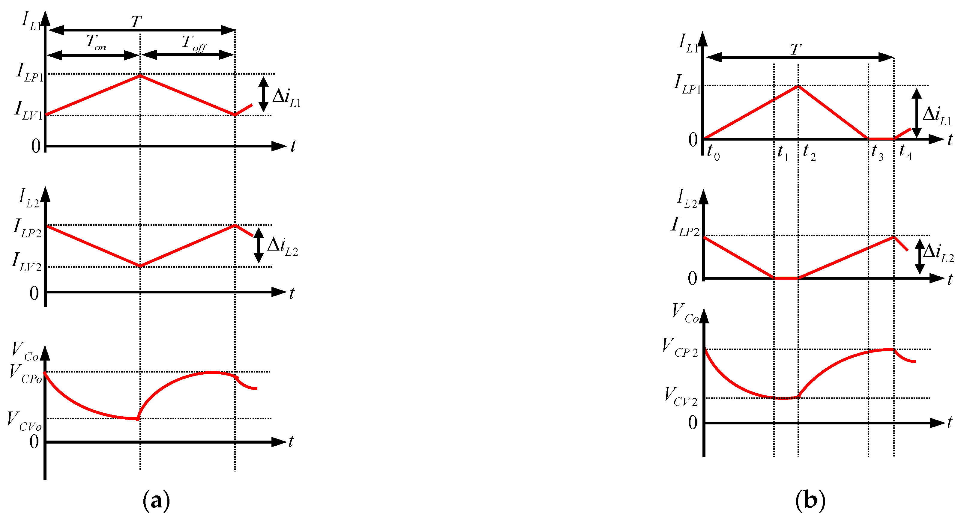
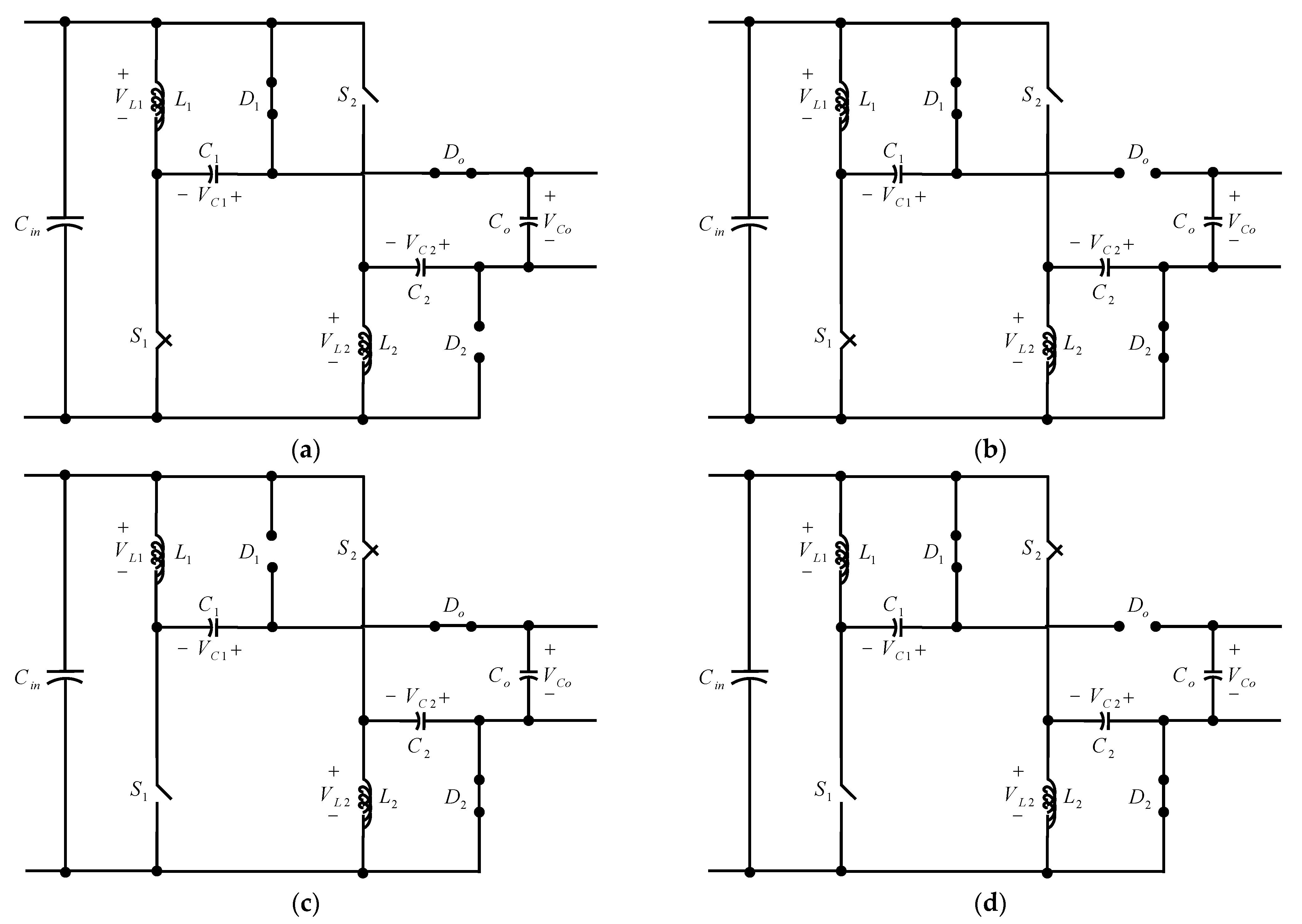
In the time interval of T o n , the switch of S 1 is turned on and the switch of S 2 is turned off. Then, the inductor L 1 is connected to the input voltage source ( V i ) and its through pass current is increased to its maximum value ( I L P 1 ) from its minimum value ( I L V 1 ) . During this time interval, the diode of D 2 is reversely biased and the diodes D 1 and D o are forward biased. In this time interval, the stored energy of the inductor L 2 is decreased to its minimum value ( I L V 2 ) from its maximum value ( I L P 2 ) . The equivalent circuit of the proposed topology is shown in Figure 2a.
This time interval of T o f f begins when the switch of S 1 is turned off and the switch of S 2 is turned on. In this situation, the diodes of D 2 and D o are turned on and the diode of D 1 is turned off. So, the inductor L 2 is connected to V i ; therefore, its stored energy is increased. Additionally, the stored energy of the capacitor C o is increased, then it is charged. The equivalent circuit of the proposed topology is shown in Figure 2b. Some key waveforms of the proposed topology in CCM are illustrated in Figure 3a.
Here, some critical relations of the proposed converter are illustrated. The first index shows the component number and second part is used for time intervals, whereas 1 and 2 show T o n and T o f f in CCM, respectively, and 1, 2, 3, and 4 show ( t 0 , t 1 ) , ( t 1 , t 2 ) , ( t 2 , t 3 ) , and ( t 3 , t 4 ) at DCM, respectively.
By applying the Kirchhoff voltage law (KVL) to the circuit of Figure 2a, the following equation is obtained:
V L 1 , 1 = V i = L 1 d i L 1 , 1 d t ,
Additionally, the equation below can be determined by Figure 2b:
V L 1 , 2 = V C 1 = L 1 d i L 1 , 2 d t ,
The equation below is also written for the inductor L 2 :
V L 2 , 1 = V C 2 , 1 = L 2 d i L 2 , 1 d t ,
V L 2 , 2 = V i = L 2 d i L 2 , 2 d t ,
By considering T = T o n + T o f f and D = T o n / T , the voltage gain of the proposed converter in CCM can be extracted by substitution (1) and (2) into voltage balance law for on inductor as follows:
V o V i = 2 D 1 D ,
Finally, D is obtained from (5) as follows:
D = 2 V i V o V i V o ,
The voltage and current relation of semiconductors and current ripples of inductors in CCM are shown in Table 1.

2.2. Analysis of the Proposed Converter in DCM

At ( t 0 , t 1 ) , the switch S 1 is turned on and the switch S 2 is turned off. Additionally, the diodes D 1 and D o are on and the diode D 2 is off. Then, the inductor L 1 is connected to V i and its stored energy is increased. Another side, the inductor L 2 is the load path, and its stored energy is decreased. Therefore, the inductor current is reached to the minimum value. The equivalent circuit of the proposed topology is shown in Figure 4a.
The time interval of ( t 1 , t 2 ) begins when the diode D o is turned off, whereas the switch S 1 is turned on and the switch S 2 is turned off. In this condition, the diode D 2 is on. So, the discharge current of the capacitor C o provides the load current and its stored energy is decreased. The equivalent circuit of the proposed topology is shown in Figure 4b.
At ( t 2 , t 3 ) , the switch S 1 is turned off and the switch S 2 is turned on. Additionally, the diodes D 2 and D o are on and the diode D 1 is off. Then, the inductor L 2 is connected to V i and its stored energy is increased. The store energy of the inductor L 1 is decreased due to its location at the load path. Therefore, the current thorough pass L 1 is reached to its minimum value. The equivalent circuit of the proposed topology is shown in Figure 4c.
At ( t 3 , t 4 ) , the switch S 1 is still turned off and the switch S 2 is turned on. Meanwhile, the diode D 2 is on, whereas the diode of D o is turned off and the diode D 1 is turned on. During this time interval, the inductor L 2 is connected to V i and is charged. Additionally, the load current is provided by the capacitor C o . The equivalent circuit of the proposed topology is shown in Figure 4d. Figure 3b shows some key waveforms of the proposed topology in DCM.
By applying KVL on Figure 4a,b, we have:
V L 1 , 2 = V i = L 1 d i L 1 , 2 d t ,
Additionally, the following equation can be written for the inductor L 1 :
V L 1 , 3 = V i + V C 1 , 3 V o = L 1 d i L 1 , 3 d t ,
V L 1 , 4 = 0 ,
From Figure 4, the equation below also results for the inductor L 2 :
V L 2 , 1 = V i + V C 2 , 1 V o = L 2 d i L 1 , 1 d t ,
V L 2 , 2 = 0 ,
V L 2 , 4 = V i = L 2 d i L 2 , 4 d t ,
By applying the voltage balance law for the inductor L 2 and replacing (7) to (9) into it, and considering D = ( t 0 , t 2 ) / T as the duty cycle in DCM, the voltage gain of the proposed converter in DCM is calculated as follows:
V o V i = 1 + 1 + D 2 R L f ,
Therefore, one obtains that:
D = V o ( 2 V i V o ) L f R V i 2 ,
Table 1 shows the voltage and current of the semiconductors and the ripple current of the inductors in this operating mode briefly.

3. Critical Inductance Calculation

In a dc-dc converter, the CCM and DCM are determined based on the values of the inductors, and the critical inductance determines the boundary between the CCM and DCM. If the inductance value of the inductors is greater than the critical inductance value, the converter will operate in CCM, and if the inductance value of the inductors is less than the critical inductance value, the converter will operate in DCM.
By replacing critical conditions into (7), the following equation is obtained:
I L P 1 = V i L 1 D T + I L V 1 ,
The equation below can be written for the capacitor:
1 T 0 T i C o d t = 0 ,
The current of the capacitor C o is equal to:
i C o , 1 = I o ,
i C o , 2 = i L 1 , 2 I o ,
Assuming a new time-off set for T o f f , the current of the inductor L 1 is equal to the following:
i L 1 , 2 = 2 V i V o 2 L t + I L P 1 ,
By replacing (18) and (17) into (16) and considering (19), the equation below is resulted:
I L P 1 = I o 1 D + V o 2 V i 4 L f ( 1 D ) ,
The above equation can be written as:
I L P 1 = I o [ 1 1 D + D ( 1 D ) R 2 L f ( 2 D ) ] ,
Substitution of the above relation into (15) yields to:
I L V 1 = I o [ 1 1 D D ( 1 D ) R 2 L f ( 2 D ) ] ,
The critical inductance of L 1 can be extracted form (22) as follows:
L C 1 = V i 2 ( V o 2 V i ) R V o ( V o V i ) 2 f ,
Assuming L 1 = L 2 , we have:
L C 2 = L C 1 ,

4. Design Considerations

The peak current flow switch (PCFS) plays a vital role in designing and selecting the type of switch, and finally, the converter price, and it can be minimized by proper selection of the inductor values. Next, the peak current of switches are extracted in CCM and DCM.

4.1. Switches Current in CCM

According to Figure 2a,b, the peak current passing through the switches are equal to:
i S P 1 = I L P 1 + i C 1 ,
i S P 2 = I L P 2 + i C 2 ,
By considering (21) and assuming L 1 = L 2 , it has resulted:
i S P 1 = i S P 2 = I o [ 1 1 D + D ( 1 D ) R 2 L f ( 2 D ) ] + i C 1 ,
By considering L 1 = L C 1 and L 2 = L C 2 into (27), the maximum peak current of the switches are determined as follows:
i S P 1 , max C C M = i S P 2 , max C C M = V o ( V o V i ) 2 R V i + V i ( V o 2 V i ) 2 L f ( V o V i ) + i C 1 ,
From the above equation, it can be concluded that the peak current passing through the switches depends on the values of D , L and R . Additionally, the maximum peak current of switches can be selected for L 1 = L C 1 and L 2 = L C 2 .

4.2. Switches Current in DCM

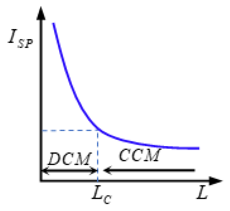
According to Figure 5, PCFSs are obtained as follows:
i S P 1 D C M = i S P 2 D C M = V i D 2 L 1 f ,
By replacing (22) into the above relation, PCFSs are rewritten as follows:
i S P 1 , min D C M = i S P 2 , min D C M = V o ( 2 V i V o ) L 1 R f ,
From the above relation, it can be seen that the minimum PCFSs in DCM also have an inverse relation with D , R and inductors values and they are obtained by considering L 1 = L C 1 and L 2 = L C 2 . The maximum PCFSs are obtained for L 1 < L C 1 and L 2 < L C 2 . Figure 5 shows the relative between the peak current of switches and inductors values. It is obvious that the peak current of switches in DCM is higher than CCM ones.
Comparing (28) and (30), it has resulted:
i S P 1 , min D C M = i S P 2 , max C C M = i S P 2 , min D C M = i S P 2 , max C C M ,

4.3. Switches Voltage Stress

From Figure 2 and Figure 4, the voltage stress of switched-off can be calculated as follows:
V S 1 = V i V C 1 ,
V S 2 = V i + V C 2

5. Efficiency Analysis

Neglecting of the inductors current ripple and the capacitors voltage ripple, the root-mean-square (RMS) current relations of inductors is given as follows:
I L 1 = I L 2 = 1 D 2 D I i ,
Thus, the inductors losses are obtained as follows:
P L 1 = r L 1 I L 1 2 + ( K f α B a c β W t f e ) ( 10 3 ) ,
P L 2 = r L 2 I L 2 2 + ( K f α B a c β W t f e ) ( 10 3 ) ,
The diodes RMS current relations are calculated as follows:
I D 1 = 1 T 0 D T ( 3 D 2 ( 2 D ) I i ) 2 d t = 3 D 2 ( 2 D ) I i D ,
I D 2 = 1 T 0 ( 1 D ) T ( 3 D 2 ( 2 D ) I i ) 2 d t = 3 D 2 ( 2 D ) I i 1 D ,
I D o = I C o + I o 1 D 2 D I i 3 ,
After neglecting turn off state losses in the diodes and defining Q r r as reverse recovery energy of diode, the diode losses are as follows:
P D 1 = V F I D 1 , a v e + r D I D 1 2 + 0.25 Q r r V D f ,
P D 2 = V F I D 2 , a v e + r D I D 2 2 + 0.25 Q r r V D f ,
P D o = V F I D o , a v e + r D I D o 2 + 0.25 Q r r V D f ,
The RMS current values of C 1 and C 2 are obtained as follows:
I C 1 = 1 T [ 0 D T ( 3 D 2 ( 2 D ) I i ) 2 d t + 0 ( 1 D ) T ( 1 D 2 ( 2 D ) I i ) 2 d t ] = I i [ 3 D 2 ( 2 D ) D + 1 D 2 ( 2 D ) 1 D ]
I C 2 = 1 T [ 0 D T ( 1 D 2 ( 2 D ) I i ) 2 d t + 0 ( 1 D ) T ( 3 D 2 ( 2 D ) I i ) 2 d t ] = I i [ 1 D 2 ( 2 D ) D + 3 D 2 ( 2 D ) 1 D ]
Considering Q C o + = Q C o , the RMS value of capacitor C o current is as follows:
I C o = 1 T [ 0 D T ( 1 D 2 D I i 6 ) 2 d t + 0 ( 1 D ) T ( 1 D 2 D I i 6 ) 2 d t ] = 1 D 2 D I i 6 ,
The capacitors losses are obtained as follows:
P C 1 = r C 1 I C 1 2 ,
P C 2 = r C 2 I C 2 2 ,
P C o = r C o I C o 2
The switches RMS current and their losses are equal to:
I S 1 = 1 T 0 D T ( 5 2 D 3 ( 2 D ) I i ) 2 d t = 5 2 D 3 ( 2 D ) I i D ,
I S 2 = 1 T 0 ( 1 D ) T ( 5 2 D 3 ( 2 D ) I i ) 2 d t = 5 2 D 3 ( 2 D ) I i 1 D ,
P S 1 = r D S o n I S 1 2 + 0.5 ( t r + t f ) I S 1 , a v e V S 1 f + 0.5 C O S S V S 1 2 f + 0.25 f Q r r , B D V S 1 + r B D 1 , I B D 1 2 + V B F 1 I B D 1 , a v e ,
P S 2 = r D S o n I S 2 2 + 0.5 ( t r + t f ) I S 2 , a v e V S 2 f + 0.5 C O S S V S 2 2 f + 0.25 f Q r r , B D V S 2 + r B D 2 , I B D 2 2 + V B F 2 I B D 2 , a v e ,
Thus, the total loss and efficiency are equal to:
P L o s s = P L 1 + P L 2 + P S 1 + P S 2 + P C 1 + P C 2 + P C o + P D 1 + P D 2 + P D o ,
η % = P o u t P o u t + P L o s s × 100 ,

6. Comparison

The comparison results of different converters avilable in the literature and the proposed converter are presented in Table 2. As shown in Table 2, the comparison is made in terms of the number of active and passive elements and the voltage gain in CCM. In terms of the number of active elements, the proposed converter topology has more switches than the ones proposed in [16] and [17]. Moreover, the proposed converter has fewer diodes than the topology in [18,19,20], and has the same number of diodes as the ones in [9,10,16,17]. Although the number of inductors of the proposed converter is less than [9,17], its number is equal to [10,16,18,19,20]. As a result, the size of the proposed converter may be smaller than the others. In terms of the number of capacitors, the proposed converter has the same number of capacitors compared to [9,16], and has less than [17,19], and more than [10,18].
Figure 6a,b show the changes in the maximum normalized voltage stress of the switch and the maximum normalized voltage stress of the diode, respectively. Except for [10], which has a fixed graph in both analyzes, the values of the maximum normalized voltage stress of the switch and the maximum normalized voltage stress of the diode change varied for different amounts of voltage gain (M). From Figure 6a, the maximum normalized voltage stress of the switch in the proposed converter is almost equal to [9], while compared to [10,16,18,19,20], the value of the maximum normalized voltage stress of the switch is lower. It is worth noting that the maximum normalized voltage stress of the switch in the proposed converter is more than [17]. The maximum normalized voltage stress of the diode at lower yields is better than the converters studied (see Figure 6b). The maximum normalized voltage stress of the diode in the proposed converter is better than [16,18,19,20], while the value of this parameter is higher compared to [9,10,17].

7. Experimental Results

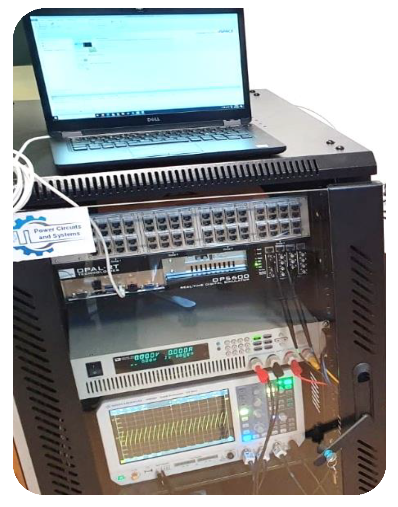
Assuming that the switches and diodes are ideal and considering the parameters presented in Table 3, the correctness of the stated theoretical concepts and relations are examined. Based on the suggested converter topology described in Section 2, a hardware-in-loop (HiL) simulating setup is configured based on the OPAL-RT real-time simulator as depicted in Figure 7. Since the HiL is developed in a real-time platform, this simulation is a more practical validation setup than an off-line MATLAB simulation for the verification of system responses to unusual events. First, the operating of the proposed converter in critical condition is carried out. Then, CCM and DCM results are recorded for the proposed converter. It should be noted that the recorded time period of the results shown is selected to show the performance of the converter in steady-state.
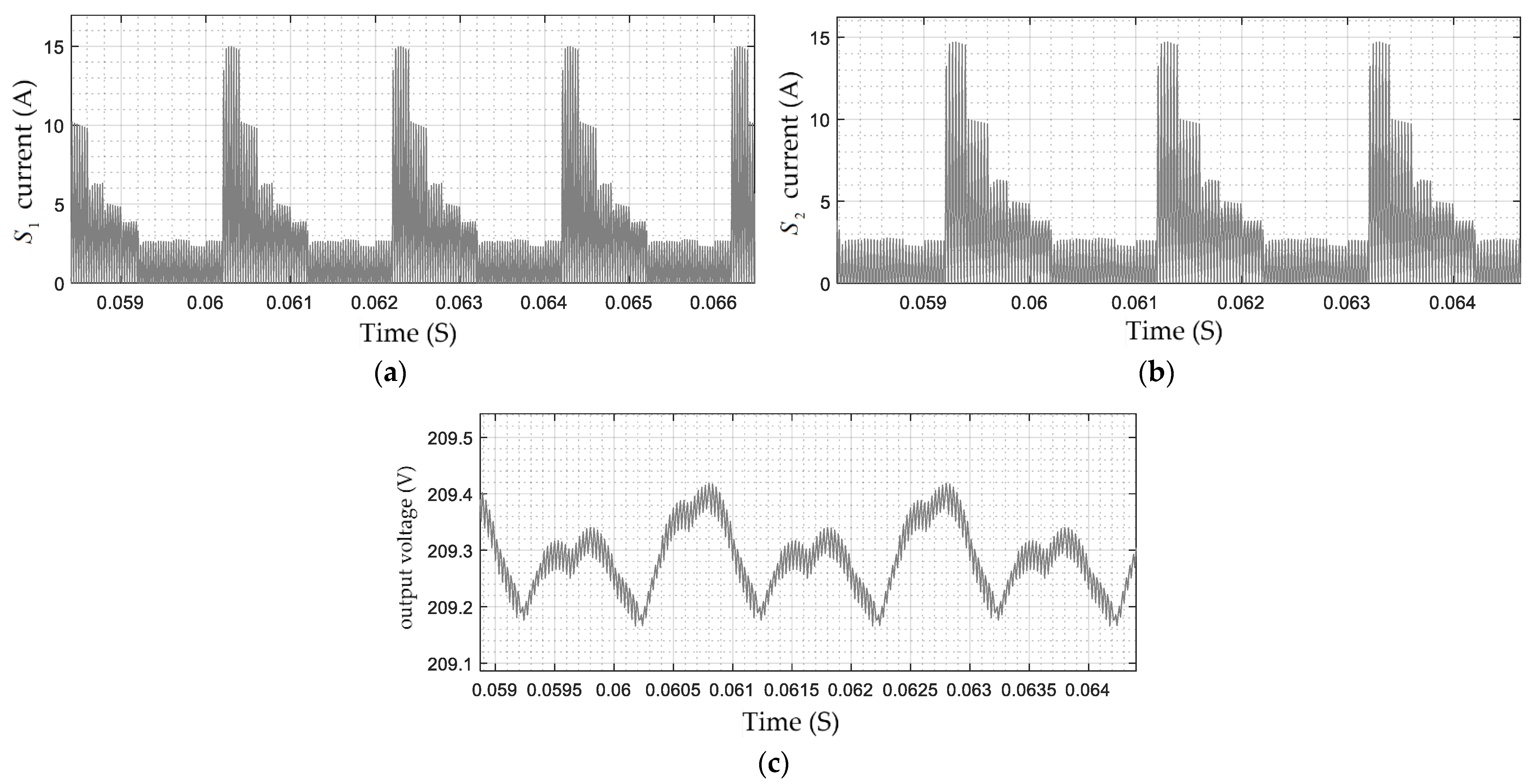
To analyze the performance of the proposed dc-dc boost converter, the operating mode of the converter must first be determined. According to (23) and Table 3, the value of critical inductances for L 1 and L 2 are equal to 256   μ H . If L 1 = L 2 > L C 1 = L C 2 , the converter will be in CCM; otherwise, it will be in DCM. The operation of the proposed converter will be in critical mode for L 1 = L 2 = L C 1 = L C 2 . The experimental results are recorded by choosing L 1 = L 2 = L C 1 = L C 2 = 256   μ H . The switch’s current waveforms are illustrated in Figure 8a,b. As one can observe from these figures, the maximum peak current of switches is 15   A . Additionally, the output voltage in this mode is equal to 209   V .
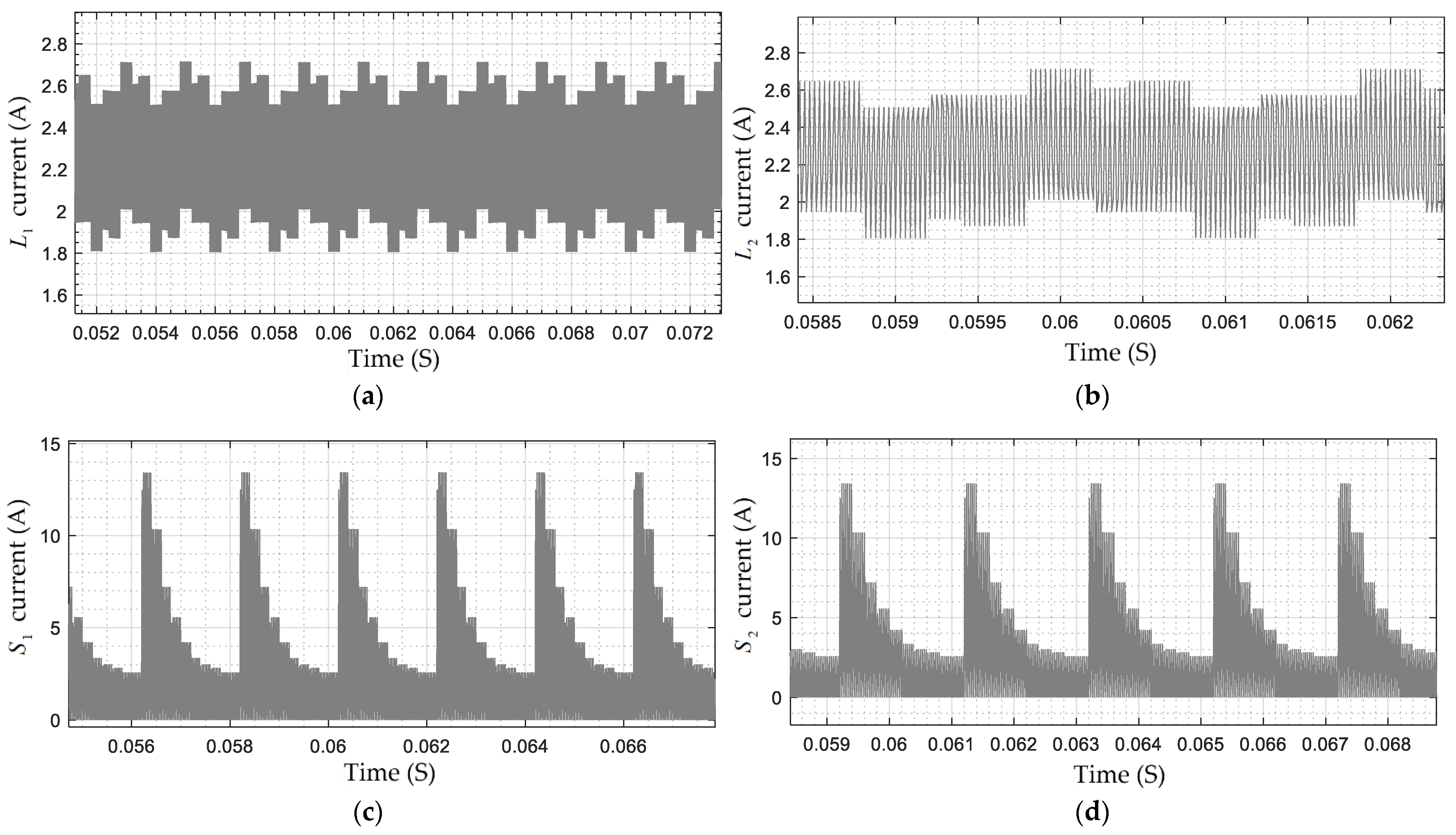
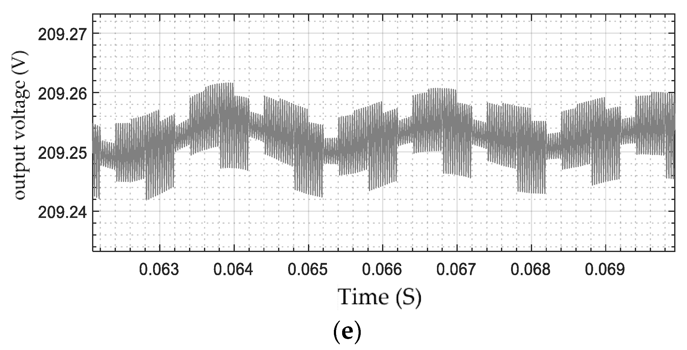
Figure 9 shows the experimental results in CCM. As shown in Figure 9a,b, the maximum peak current of the inductors is 2.7   A ; hence, the inductor size can be reduced. It can be noted that Δ i L 1 = Δ i L 2 = 1   A . The switches’ current waveforms are shown in Figure 9c,d, while their maximum values are 13   A according to (25) to (28). The output voltage is almost equal to 209   V , reconfirming the theoretical calculation (see Figure 9e).
Considering the presented parameters in Table 3 into (34) and (52), powder core inductor ( r L 1 = r L 2 = 0.08   Ω ; K = 0.00551 ; α = 1.23 ; β = 2.12 ; W t f e = 34.6 ; B a c = 0.0527 ), electrolytic capacitor ( r C 1 = r C 2 = 0.015   Ω ; r C o = 0.02   Ω ), N-channel MOSFET ( Type : STW 45 NM 5 0 F ; r D S o n = 0.07   Ω ; t r = 28   nS ; t f = 25   nS ; C O S S = 1260   pF ; Q r r = 1600   nC ; d i / d t = 100   A / μ S ), diodes ( Type : MUR 1560 ; V F , D = 0.8   V ; r D = 0.01   Ω ) and neglecting from the third term of the diodes losses relations and fifth and sixth term of switch losses relations yields P L 1 = P L 2 = 0.72   W , P D 1 = P D 2 = 6.3   W , P D o = 0.816   W , P C 1 = P C 2 = 1.6   W , P C o = 0.01   W and P S 1 = P S 2 = 6.0543   W . Thus, the calculated efficiency is 93.1 % .
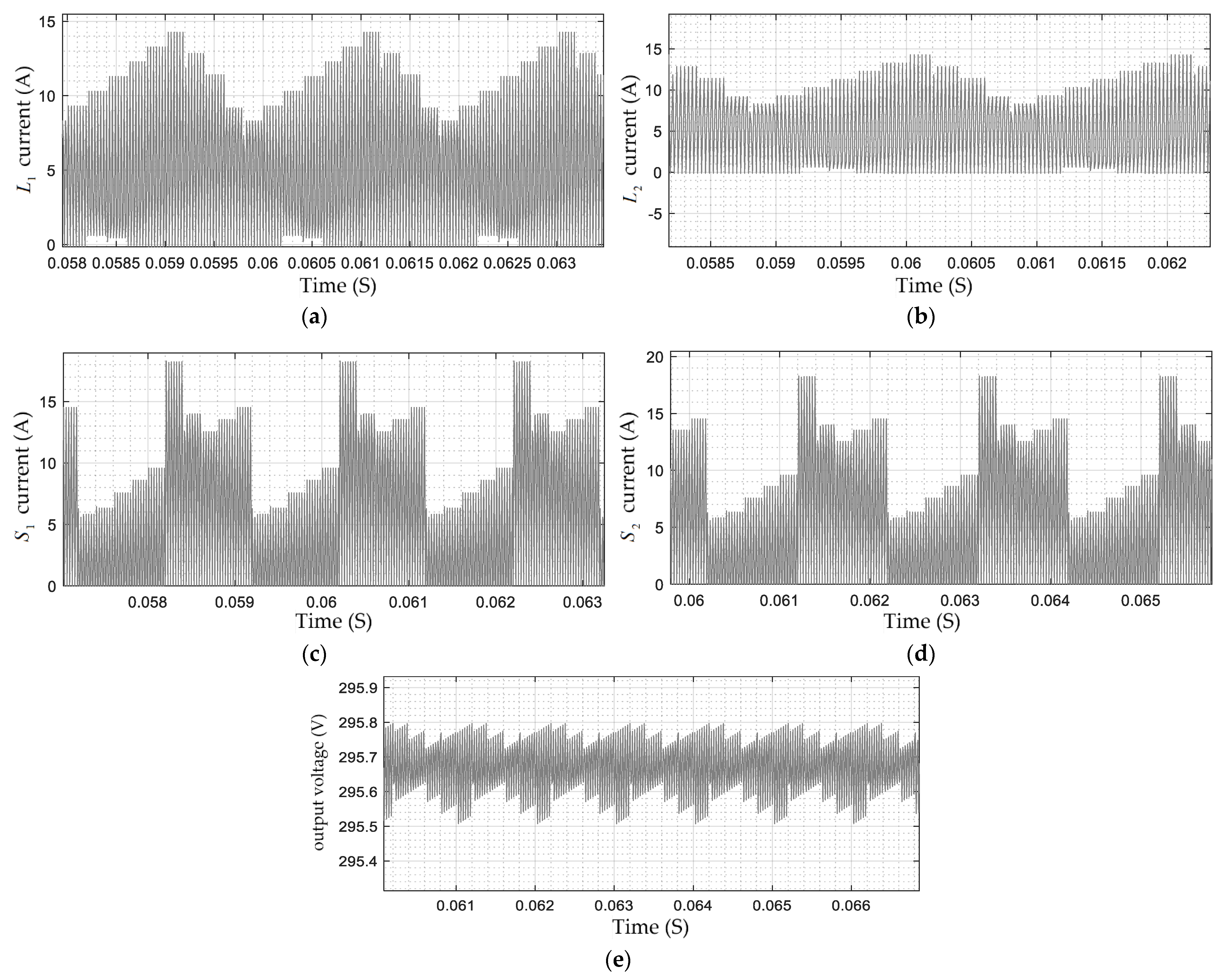
The results in DCM are depicted in Figure 10. The inductors’ currents are illustrated in Figure 10a,b. As shown in these figures, their variation proves the theorical relations and their maximum values are 14   A . The switch current also reached 17   A (see Figure 10c–e shows the output voltage value, which is equal to 295   V .

8. Conclusions

In this paper, a new topology of a non-isolated boost dc-dc converter is proposed for the off-board EV charger. High voltage gain and high-frequency transformer-less are the main advantages of the proposed topology. Throughout this paper, the operation of the proposed converter was analyzed at CCM and DCM in detail. Additionally, the critical inductance calculations were carried out, and the designing considerations were extracted for choosing proper switches. Then, the proposed converter was compared with the existing topologies in the literature. The validity of the correctness of the theoretical concepts was verified through HiL setup based on the OPAL-RT simulator. As discussed in Section 2, the output voltage increased to 210   V and 295   V at CCM and DCM, respectively, by D = 50 % , V i = 70   V and f = 30.5 kHz with the calculated efficiency equal to 93.1 % . Additionally, the maximum peak current of switches reached 15   A , 13   A and 17   A at critical mode, CCM and DCM, respectively. Therefore, the proposed topology can be a suitable appliance as an EV charger.

Author Contributions

F.M.S., Methodology; M.G., Software; M.S.S., Supervision; M.-H.K.; Validation. All authors have read and agreed to the published version of the manuscript.

Funding

This research received no external funding.

Conflicts of Interest

The authors declare no conflict of interest.

References

  1. Iyer, V.M.; Gulur, S.; Gohil, G.; Bhattacharya, S. An Approach Towards Extreme Fast Charging Station Power Delivery for Electric Vehicles with Partial Power Processing. IEEE Trans. Ind. Electron. 2019, 67, 8076–8087. [Google Scholar] [CrossRef]
  2. Ucer, E.; Koyuncu, I.; Kisacikoglu, M.C.; Yavuz, M.; Meintz, A.; Rames, C. Modeling and Analysis of a Fast Charging Station and Evaluation of Service Quality for Electric Vehicles. IEEE Trans. Transp. Electron. 2019, 5, 215–225. [Google Scholar] [CrossRef]
  3. Rafiei, M.; Boudjadar, J.; Khooban, M.-H. Energy Management of a Zero-Emission Ferry Boat With a Fuel-Cell-Based Hybrid Energy System: Feasibility Assessment. IEEE Trans. Ind. Electron. 2021, 68, 1739–1748. [Google Scholar] [CrossRef]
  4. Tu, H.; Feng, H.; Srdic, S.; Lukic, S. Extreme Fast Charging of Electric Vehicles: A Technology Overview. IEEE Trans. Transp. Electron. 2019, 5, 861–878. [Google Scholar] [CrossRef]
  5. Khooban, M.-H. An Optimal Non-Integer Model Predictive Virtual Inertia Control in Inverter-Based Modern AC Power Grids-Based V2G Technology. IEEE Trans. Energy Convers. 2021, 36, 1336–1346. [Google Scholar] [CrossRef]
  6. Metwly, M.Y.; Abdel-Majeed, M.S.; Abdel-Khalik, A.S.; Hamdy, R.A.; Hamad, M.S.; Ahmed, S. A Review of Integrated On-Board EV Battery Chargers: Advanced Topologies, Recent Developments and Optimal Selection of FSCW Slot/Pole Combination. IEEE Access 2020, 8, 85216–85242. [Google Scholar] [CrossRef]
  7. Srdic, S.; Lukic, S. Toward extreme fast charging: Challenges and opportunities in directly connecting to medium-voltage line. IEEE Electrif. Mag. 2019, 7, 22–31. [Google Scholar] [CrossRef]
  8. Yilmaz, M.; Krein, P.T. Review of battery charger topologies, charging power levels, and infrastructure for plug-in electric and hybrid vehicles. IEEE Trans. Power Electron. 2013, 28, 2151–2169. [Google Scholar] [CrossRef]
  9. Banaei, M.R.; Sani, S.G. Analysis and implementation of a new sepic-based single-switch buck-boost dc-dc converter with continuous input current. IEEE Trans. Power Electron. 2018, 33, 10317–10325. [Google Scholar] [CrossRef]
  10. Shahir, F.M.; Babaei, E.; Farsadi, M. Extended topology for boost dc-dc converter. IEEE Trans. Power Electron. 2019, 34, 2375–2384. [Google Scholar] [CrossRef]
  11. Aggeler, D.; Canales, F.; Zelaya-De La Parra, H.; Coccia, A.; Butcher, N.; Apeldoorn, O. Ultra-Fast Dc-Charge Infrastructures for Ev-Mobility and Future smart Grids. In Proceedings of the IEEE PES Innovative Smart Grid Technologies Conference Europe (ISGT Europe), Gothenburg, Sweden, 11–13 October 2010; pp. 1–8. [Google Scholar]
  12. Garcia, O.; Zumel, P.; de Castro, A.; Cobos, A. Automotive dc-dc bidirectional converter made with many interleaved buck stages. IEEE Trans. Power Electron. 2006, 21, 578–586. [Google Scholar] [CrossRef]
  13. Kang, T.; Kim, C.; Suh, Y.; Park, H.; Kang, B.; Kim, D. A design and control of bi-directional non-isolated dc-dc converter for rapid electric vehicle charging system. In Proceedings of the Twenty-Seventh Annual IEEE Applied Power Electronics Conference and Exposition (APEC), Orlando, FL, USA, 5–9 February 2012; pp. 14–21. [Google Scholar]
  14. Zhang, J.; Lai, J.; Kim, R.; Yu, W. High-power density design of a soft-switching high-power bidirectional dc-dc converter. IEEE Trans. Power Electron. 2007, 22, 1145–1153. [Google Scholar] [CrossRef]
  15. Christen, D.; Jauch, F.; Biel, J. Ultra-fast charging station for electric vehicles with integrated split grid storage. In Proceedings of the 17th European Conference on Power Electronics and Applications (EPE’15 ECCE-Europe), Geneva, Switzerland, 8–10 September 2015; pp. 1–11. [Google Scholar]
  16. Shahir, F.M.; Babaei, E.; Farsadi, M. Voltage-lift technique based non-isolated boost dc-dc converter: Analysis and design. IEEE Trans. Power Electron. 2018, 33, 5917–5926. [Google Scholar] [CrossRef]
  17. Salvador, M.A.; Lazzarin, T.B.; Coelho, R.F. High step-up dc-dc converter with active switched-inductor and passive switched-capacitor networks. IEEE Trans. Ind. Electron. 2018, 65, 5644–5654. [Google Scholar] [CrossRef]
  18. Shahir, F.M.; Babaei, E.; Farsadi, M. Analysis and design of voltage-lift technique based non-isolated boost dc-dc converter. IET Power Electron. 2018, 11, 1083–1091. [Google Scholar] [CrossRef]
  19. Zhou, L.; Zhu, B.; Lou, Q.; Chen, S. Interleaved non-isolated high step-up dc/dc converter based on the diode-capacitor multiplier. IET Power Electron. 2014, 7, 390–397. [Google Scholar] [CrossRef]
  20. Pan, C.T.; Chuang, C.F.; Chu, C.C. A novel transformer-less adapt-able voltage quadrupler dc converter with low switch voltage stress. IEEE Trans. Power Electron. 2014, 29, 4787–4796. [Google Scholar] [CrossRef]
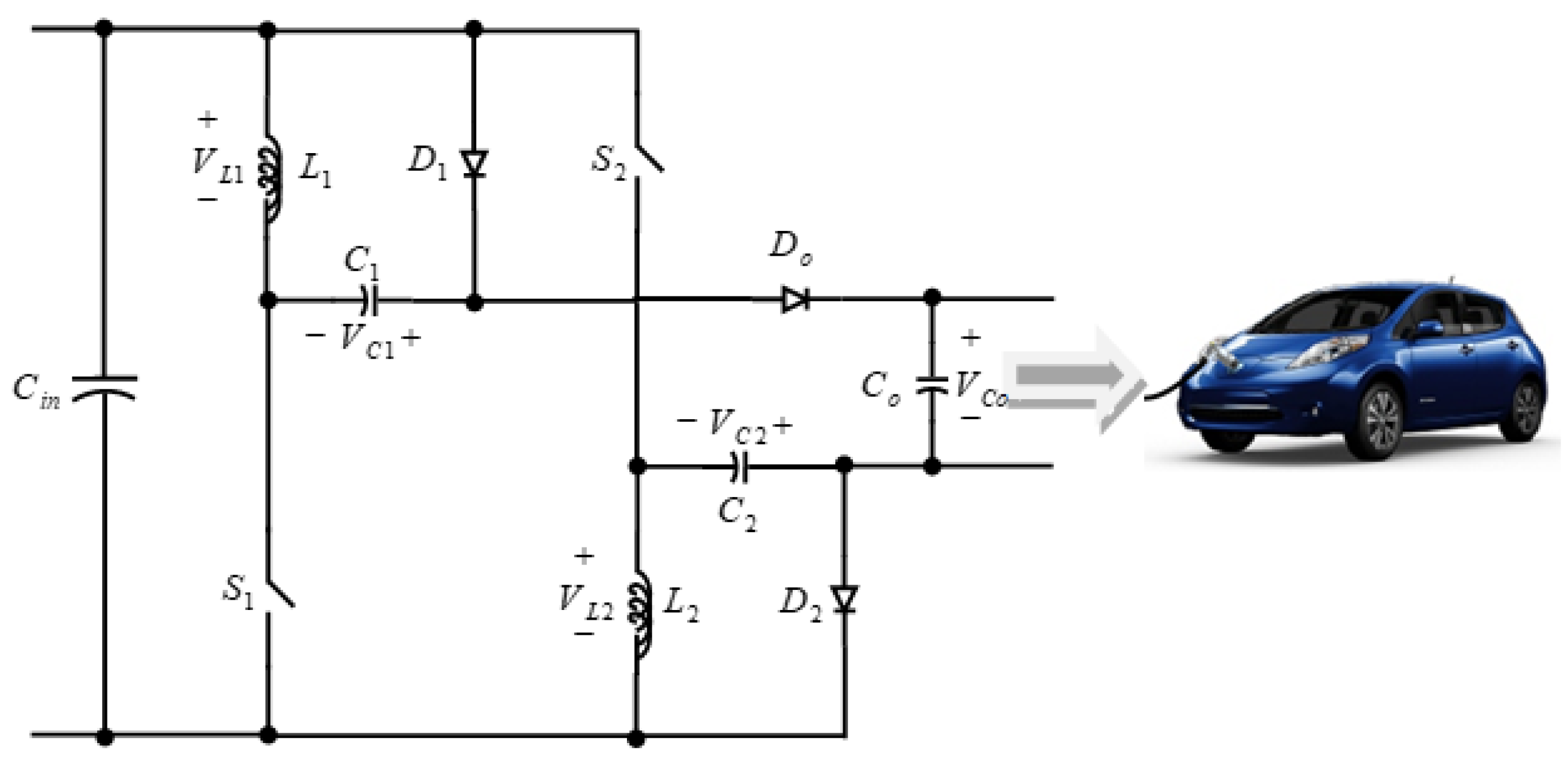
Figure 1. The proposed topology for the boost dc-dc converter.
Designs 05 00051 g001
Figure 2. The equivalent circuit of the proposed topology in CCM; (a) at T o n , (b) at T o f f .
Designs 05 00051 g002
Figure 3. Some key waveforms of the proposed topology; (a) at CCM, (b) at DCM.
Designs 05 00051 g003
Figure 4. The equivalent circuit of the proposed topology in DCM; (a) at ( t 0 , t 1 ) , (b) at ( t 1 , t 2 ) , (c) at ( t 2 , t 3 ) , (d) at ( t 3 , t 4 ) .
Designs 05 00051 g004
Figure 5. The relation between the value of the inductances and PCFS.
Designs 05 00051 g005
Figure 6. The maximum normalized voltage stress for (a) switch and (b) diode.
Designs 05 00051 g006
Figure 7. Photograph of the OPAL-RT setup adopted for the HiL verification.
Designs 05 00051 g007
Figure 8. The results in critical mode, (a) S 1 current, (b) S 2 current, and (c) output voltage.
Designs 05 00051 g008
Figure 9. The results in CCM, (a) L 1 current, (b) L 2 current, (c) S 1 current, (d) S 2 current, and (e) output voltage.
Designs 05 00051 g009aDesigns 05 00051 g009b
Figure 10. The results in DCM, (a) L 1 current, (b) L 2 current, (c) S 1 current, (d) S 2 current, and (e) output voltage.
Designs 05 00051 g010
Table 1. Comparison between proposed converter and the existing topologies.
Elements/Time IntervalCCMDCM
T o n T o f f t 0 t 1 t 1 t 2 t 2 t 3 t 3 t 4
D 1 i C 1 + I o + i C o V L 1 V C 1 i C 1 + I o + i C o i C 1 + I o + i C o V L 1 V C 1 i C 1 + I o + i C o
D 2 V L 2 + V C 2 I o + i C o i C 2 V L 2 + V C 2 I o + i C o i C 2 I o + i C o i C 2 I o + i C o i C 2
D o I o + i C o I o + i C o V i V o I o + i C o V i V o
S 1 i L 1 + i C 1 V i V L 1 i L 1 + i C 1 V i V L 1 V i
S 2 V i V L 2 I i i L 1 V i V L 2 V i I i i L 1 I i i D 1
Δ i L 1 | V i L 1 T o n | = | V C 1 L 1 T o f f | | V i L 1 Δ t | = | V i + V C 1 , 3 V o L 1 Δ t |
Δ i L 2 | V C 2 , 1 L 2 T o n | = | V i L 2 T o f f | | V i + V C 2 , 1 V o L 2 Δ t | = | V i L 2 Δ t |
Table 2. Comparison between proposed converter and the existing topologies.
Elements/Ref.[9][10][16][18][19][20][17]Proposed
Switch22122212
Inductor32222242
Capacitor32324463
Diode23344533
Voltage gain in CCM 1 + 3 D 1 D 1 D ( 1 D ) 1 + D 1 D 1 + D D ( 1 D ) 4 1 D 4 1 D 3 D 1 D 2 D 1 D
Max. Nor. voltage of switch M + 3 2 M 1 M + 1 2 2 M + 2 3 M M 4 M 4 M + 3 3 M 3 M 4 2 M 3
Max. Nor. voltage of diode M + 3 2 M 3 2 + 1 4 1 M M + 1 2 1 + M + 2 M 2 M 2 M + 3 3 M M 1 3
Table 3. Parameters for the proposed converter topology.
ParametersCCMDCM
Duty   cycle D = 50 % D = 50 %
R 100   Ω 100   Ω
L 1 = L 2 1   m H 70   μ H
C 1 = C 2 47   μ F 47   μ F
C o 100   μ F 100   μ F
V i ,   f 70   V ,   33.5   kHz 70   V ,   33.5   kHz
Publisher’s Note: MDPI stays neutral with regard to jurisdictional claims in published maps and institutional affiliations.