Lighting Control via Magnetic Field Communication

Abstract
:
1. Introduction
2. Adjustable Isolated Driver
3. Signal Modulation
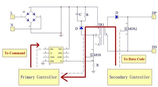
4. Structure
5. Control Design
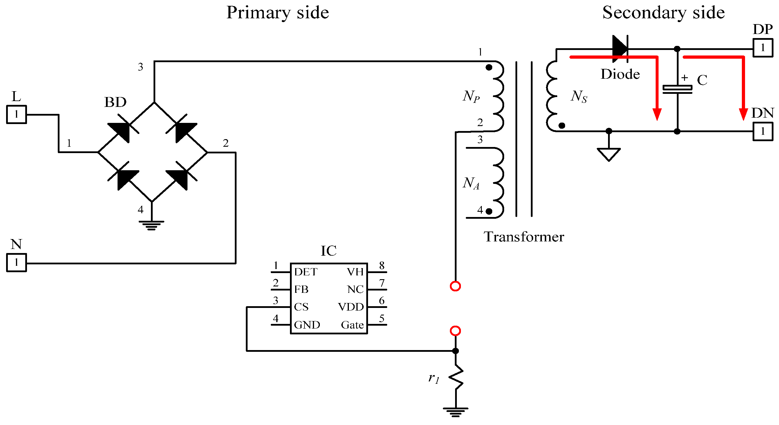
5.1. Transformer
5.2. Driver and Controller
5.3. Coding and Decoding Schemes
6. Experimental Results
6.1. Performance Test
6.2. Communication Quality Test
6.3. Efficiency Test
7. Discussion
8. Conclusions
9. Patent
Author Contributions
Funding
Conflicts of Interest
References
- Jenkins, D.; Bhargava, A. LED Lighting: Maximizing the Reliability, Safety, and Efficiency of Light Fixtures in Hazardous Environments. IEEE Ind. Appl. Mag. 2015, 21, 64–67. [Google Scholar]
- Lyu, X.; Li, Y.; Liu, G.; Cao, D. A High-Efficiency Linear LED Driver with Concave Current Control for Low-Power Application. IEEE J. Emerg. Sel. Top. Power Electron. 2015, 3, 691–697. [Google Scholar] [CrossRef]
- Anghel, V.; Bartholomeusz, C.; Vasilica, A.G.; Pristavu, G.; Brezeanu, G. Variable Off-Time Control Loop for Current-Mode Floating Buck Converters in LED Driving Applications. IEEE J. Solid-State Circuits 2014, 49, 1571–1579. [Google Scholar]
- Hsieh, Y.T.; Juang, Y.Z. Analysis and Suppression of Overcurrent in Boost LED Drivers. J. Disp. Technol. 2013, 9, 388–395. [Google Scholar]
- Hsieh, Y.T.; Liu, B.D.; Wu, J.F.; Fang, C.L.; Tsai, H.H.; Juang, Y.Z. A High Current Accuracy Boost White LED Driver Based on Offset Calibration Technique. IEEE Trans. Circuits Syst. 2011, 58, 244–248. [Google Scholar]
- Wang, Y.; Guan, Y.; Huang, J.; Wang, W.; Xu, D. A Single-Stage LED Driver Based on Interleaved Buck–Boost Circuit and LLC Resonant Converter. IEEE J. Emerg. Sel. Top. Power Electron. 2015, 3, 732–741. [Google Scholar] [CrossRef]
- Luo, Q.; Huang, J.; He, Q.; Ma, K.; Zhou, L. Analysis and Design of a Single-Stage Isolated AC–DC LED Driver with a Voltage Doubler Rectifier. IEEE Trans. Ind. Electron. 2017, 64, 5807–5817. [Google Scholar]
- Lam, J.C.W.; Jain, P.K. Isolated AC/DC Offline High Power Factor Single-Switch LED Drivers without Electrolytic Capacitors. IEEE J. Emerg. Sel. Top. Power Electron. 2015, 3, 679–690. [Google Scholar]
- Tan, Y.K.; Huynh, T.P.; Wang, Z. Smart Personal Sensor Network Control for Energy Saving in DC Grid Powered LED Lighting System. IEEE Trans. Smart Grid 2013, 4, 669–676. [Google Scholar]
- Daely, P.T.; Reda, H.T.; Satrya, G.B.; Kim, J.W.; Shin, S.Y. Design of Smart LED Streetlight System for Smart City with Web-Based Management System. IEEE Sens. J. 2017, 17, 6100–6110. [Google Scholar]
- Lai, K.K.; Hung, T.S.; Hsu, M.Y.; Lin, W.T. An Innovative Model of Blue Ocean Strategy and Niche Marketing in Green Industry: A Case Study of the Smart LED Industry. In Proceedings of the 2011 PICMET 11, Technology Management in the Energy Smart World, Portland, OR, USA, 31 July–4 August 2011; pp. 1–7. [Google Scholar]
- Ran, L.; Zhang, X.; Zhao, C.; Hu, H.; Luo, L. Preliminary Exploration on Visual Ergonomics in LED Illumination and National Standard System Framework for Visual Ergonomics. In Proceedings of the 2013 10th China International Forum on Solid State Lighting, Beijing, China, 10–12 November 2013; pp. 198–201. [Google Scholar]
- Magno, M.; Polonelli, T.; Benini, L.; Popovici, E. A Low Cost, Highly Scalable Wireless Sensor Network Solution to Achieve Smart LED Light Control for Green Buildings. IEEE Sens. J. 2015, 15, 2963–2973. [Google Scholar]
- Huang, C.C.; Lin, C.L.; Wu, Y.K. Simultaneous Wireless Power/Data Transfer for Electric Vehicle Charging. IEEE Trans. Ind. Electron. 2017, 64, 682–690. [Google Scholar]
- Caponetto, R.; Dongola, G.; Fortuna, L.; Riscica, N.; Zufacchi, D. Power Consumption Reduction in A Remote Controlled Street Lighting System. In Proceedings of the 2008 International Symposium on Power Electronics, Electrical Drivers Automation and Motion, Ischia, Italy, 11–13 June 2008; pp. 428–433. [Google Scholar]
- Sadiku, M.N.O. Elements of Electromagnetics, 6th ed.; Oxford University Press Inc.: New York, NY, USA, 2014; ISBN 978-0-1993-2140-7. [Google Scholar]
- Rao, N.N. Elements of Engineering Electromagnetics, 6th ed.; Prentice Hall: Upper Saddle River, NJ, USA, 2004; ISBN 978-0-1311-3961-9. [Google Scholar]
- Huang, C.C.; Lin, C.L. Wireless Power and Bidirectional Data Transfer Scheme for Battery Charger. IEEE Trans. Power Electron. 2018, 33, 4679–4689. [Google Scholar]
- Texas Instruments. Available online: http://www.ti.com/. (accessed on 1 March 2019).
- Zhang, J.; Zeng, H.; Jiang, T. A Primary-Side Control Scheme for High-Power-Factor LED Driver with TRIAC Lighting Capability. IEEE Trans. Power Electron. 2012, 27, 4619–4629. [Google Scholar]
- Moon, S.C.; Koo, G.B.; Moon, G.W. A New Control Method of Interleaved Single-Stage Flyback AC–DC Converter for Outdoor LED Lighting Systems. IEEE Trans. Power Electron. 2013, 28, 4051–4062. [Google Scholar]
- Hwang, J.T.; Jung, M.S.; Kim, D.H.; Lee, J.H.; Jung, M.H.; Shin, J.H. Off-the-Line Primary Side Regulation LED Lamp Driver with Single-Stage PFC and TRIAC Dimming Using LED Forward Voltage and Duty Variation Tracking Control. IEEE J. Solid-State Circuits 2012, 47, 3081–3094. [Google Scholar]
- Haykin, S.; Moher, M. Communication Systems, 5th ed.; John Wiley & Sons, Inc.: Hoboken, NJ, USA, 2010; ISBN 978-0-4716-9790-9. [Google Scholar]
- ON Semiconductor. Available online: https://www.onsemi.com/. (accessed on 17 March 2019).
- STMicroelectronics. Available online: https://www.st.com/content/st_com/en.html. (accessed on 19 March 2019).
- Ferroxcube. Available online: https://www.ferroxcube.com/en-global/home/index. (accessed on 19 March 2019).
- Shilyashki, G.; Pfützner, H.; Anger, J.; Gramm, K.; Hofbauer, F.; Galabov, V.; Mulasalihovic, E. Magnetostriction of Transformer Core Steel Considering Rotational Magnetization. IEEE Trans. Magn. 2014, 50, 16. [Google Scholar] [CrossRef]


| Proposed Method | Previous Approach [13] | |
|---|---|---|
| Communication Architecture | Embedded in flyback driver | External RF device needed |
| Controller and Driver | Integrated design | Separated design |
| Hardware cost | Comparatively low [18] | Comparatively high |
| Number of Layers | Winding | Pin (S→F) | Wire Diameter (ψ) | Number of Turns (T) |
|---|---|---|---|---|
| 1 | NP1 | 12→1 | 0.25 | 33 |
| 2 | Insulation Tape | 3 | ||
| 3 | NS | 7→8 | 0.25 × 2 | 19 |
| 4 | Insulation Tape | 3 | ||
| 5 | NP2 | 1→2 | 0.25 | 32 |
| 6 | Insulation Tape | 3 | ||
| 7 | NA | 6→5 | 0.25 | 19 |
| 8 | Insulation Tape | 3 | ||
| Output Current Changes | |||
| Pin (W) | Vout (V) | Iout (A) | η (%) |
| 14.2 | 19 | 0.64 | 85.63 |
| 3.5 | 18.6 | 0.16 | 85.03 |
| 1.7 | 18 | 0.08 | 84.71 |
| Output Voltage Changes | |||
| Pin (W) | Vout (V) | Iout (A) | η (%) |
| 9.74 | 13 | 0.632 | 84.35 |
| 7.78 | 10 | 0.63 | 80.98 |
| 5.7 | 7 | 0.63 | 77.37 |
| Designed LED Lighting System | |||||
| Modulation | Pin (W) | Vout (V) | Iout (A) | Pout (W) | Efficiency (%) |
| M1 | 15.12 | 18.8 | 0.72 | 13.54 | 89.52% |
| M2 | 13.86 | 18.6 | 0.66 | 12.28 | 88.57% |
| M3 | 12.60 | 18.4 | 0.61 | 11.22 | 89.08% |
| M4 | 11.34 | 18.2 | 0.55 | 10.01 | 88.27% |
| M5 | 10.08 | 18.0 | 0.49 | 8.82 | 87.50% |
| M6 | 8.82 | 17.8 | 0.43 | 7.65 | 86.78% |
| M7 | 7.56 | 17.6 | 0.37 | 6.51 | 86.14% |
| M8 | 6.30 | 17.4 | 0.32 | 5.57 | 88.38% |
| M9 | 5.04 | 17.2 | 0.25 | 4.30 | 85.32% |
| M10 | 3.78 | 17.0 | 0.19 | 3.23 | 85.45% |
| Buck-boost LED Lighting System | |||||
| Modulation | Pin (W) | Vout (V) | Iout (A) | Pout (W) | Efficiency (%) |
| M1 | 38.22 | 20.3 | 1.57 | 31.87 | 83.38% |
| M2 | 32.24 | 19.8 | 1.35 | 26.73 | 82.91% |
| M3 | 27.90 | 19.3 | 1.19 | 22.97 | 82.32% |
| M4 | 23.87 | 18.8 | 1.03 | 19.36 | 81.12% |
| M5 | 18.91 | 18.3 | 0.82 | 15.01 | 79.35% |
| M6 | 14.26 | 17.8 | 0.63 | 11.21 | 78.64% |
| M7 | 10.23 | 17.3 | 0.46 | 7.96 | 77.79% |
| M8 | 6.20 | 16.8 | 0.28 | 4.70 | 75.87% |
| M9 | 3.72 | 16.3 | 0.17 | 2.77 | 74.49% |
| M10 | 1.24 | 15.8 | 0.04 | 0.63 | 50.97% |
© 2019 by the authors. Licensee MDPI, Basel, Switzerland. This article is an open access article distributed under the terms and conditions of the Creative Commons Attribution (CC BY) license (http://creativecommons.org/licenses/by/4.0/).
Share and Cite
Kao, J.-J.; Lin, C.-L.; Huang, C.-C.; Huang, C.-H. Lighting Control via Magnetic Field Communication. Inventions 2019, 4, 70. https://doi.org/10.3390/inventions4040070
Kao J-J, Lin C-L, Huang C-C, Huang C-H. Lighting Control via Magnetic Field Communication. Inventions. 2019; 4(4):70. https://doi.org/10.3390/inventions4040070
Chicago/Turabian StyleKao, Jia-Jing, Chun-Liang Lin, Chih-Cheng Huang, and Chung-Hsin Huang. 2019. "Lighting Control via Magnetic Field Communication" Inventions 4, no. 4: 70. https://doi.org/10.3390/inventions4040070