Article

Additive Manufacturing of Side-Coupled Cavity Linac Structures from Pure Copper: A First Concept

1
Institute for Applied Physics and Measurement Technology (LRT2), Universität der Bundeswehr München, Werner-Heisenberg-Weg 39, 85577 Neubiberg, Germany
2
Institute for Design and Production Engineering, Universität der Bundeswehr München, Werner-Heisenberg-Weg 39, 85577 Neubiberg, Germany
3
Fraunhofer-Institut für Werkstoff- und Strahltechnik IWS, Winterbergstraße 28, 01277 Dresden, Germany
4
Institute of Microwaves and Photonics (LHFT), Friedrich-Alexander Universität Erlangen–Nürnberg (FAU), Schloßplatz 4, 91054 Erlangen, Germany
*
Author to whom correspondence should be addressed.
Instruments 2023, 7(4), 56; https://doi.org/10.3390/instruments7040056
Submission received: 6 November 2023 / Revised: 7 December 2023 / Accepted: 12 December 2023 / Published: 14 December 2023

Abstract

:
Compared to conventional manufacturing, additive manufacturing (AM) of radio frequency (RF) cavities has the potential to reduce manufacturing costs and complexity and to enable higher performance. This work evaluates whether normal conducting side-coupled linac structures (SCCL), used worldwide for a wide range of applications, can benefit from AM. A unit cell geometry (SC) optimized for 75 MeV protons was developed. Downskins with small downskin angles α were avoided to enable manufacturing by laser powder bed fusion without support structures. SCs with different α were printed and post-processed by Hirtisation (R) (an electrochemical process) to minimize surface roughness. The required accuracy for 3 GHz SCCL (medical linacs) is achieved only for α > 45 . After a material removal of 140 µm due to Hirtisation (R), a quality factor Q 0 of 6650 was achieved. This corresponds to 75% of the Q 0 simulated by CST®. A 3 GHz SCCL concept consisting of 31 SCs was designed. The effective shunt impedance Z T 2 simulated by CST corresponds to 60.13 M Ω m and is comparable to the Z T 2 of SCCL in use. The reduction in Z T 2 expected after Hirtisation (R) can be justified in practice by up to 70% lower manufacturing costs. However, future studies will be conducted to further increase Q 0 .

1. Introduction

Particle accelerators are sophisticated devices used to accelerate charged particles, such as electrons or protons, to high energies, respectively velocities up to c 0 [1]. They play a crucial role in diverse scientific disciplines, including particle physics, nuclear physics, and accelerator-based research. Additionally, they find practical applications in medical treatments like radiation therapy for cancer, industrial material analysis and processing, and advanced imaging techniques [1,2,3,4,5]. Linear particle accelerators (hereinafter: linacs) account for the largest share of the more than 35,000 particle accelerators worldwide [6]. The fundamental components of most linacs are radio frequency (RF) cavities (hereinafter: cavities). Cavities are structures made of highly conductive materials (e.g., aluminum, copper, their alloys, or superconductors) that enclose an open volume. If an electromagnetic sinusoidal alternating signal (RF signal) with a frequency corresponding to the resonance frequency f R defined by the cavity geometry is coupled into the cavity, high-grade electromagnetic (EM) fields result in the cavity. Thus, electric field components of up to around 100 MV m can be generated in cavities to efficiently accelerate charged particles [1].
To realize maximum acceleration, cavities usually have complex internal geometries, such as drift tubes, to shield the particle from unwanted field phases and concentrate the E-field on the beam axis. Additionally, cavities are equipped with cooling channels to ensure stable operation of the cavity at high input powers [1]. Using conventional machining, cavities can often only be produced in individual parts due to these complex geometries. However, optimum electrical conductivity and vacuum suitability are essential. Therefore, the individual parts must be joined using processes such as brazing, electron beam welding, etc. The manufacture of most modern cavities requires the precise sequential execution of several machining and joining steps. The conventional manufacturing process limits the freedom in design and is a major source of potential defects. It limits the realization of new innovative cavity concepts for a new generation of resource-saving linacs with higher performance (less energy consumption, longer operating times, etc.) [6,7,8,9]. In addition, depending on, e.g., particle type, particle velocity, and required beam current, different cavity geometries are used for each application, but also within one accelerator structure. Cavities are therefore always single pieces or, at best, small series. As a result, cavities and therefore the conventional manufacturing process account for up to 25% of the investment cost of linacs.
Additive manufacturing (AM) or 3D printing offers several advantages over conventional manufacturing processes. AM enables the production of more complex geometries that were previously not feasible. This design freedom results in optimized components with improved performance characteristics. AM eliminates the need for expensive tooling and molds and reduces material waste. In addition, AM enables decentralized, on-demand production and accelerates product development cycles through rapid prototyping [10,11].
As a result of continuous improvements since the 1980s, additive manufacturing processes are now being considered for the manufacturing of RF cavities. Cavity prototypes already fully or partially manufactured by AM include a radio frequency quadrupole cavity (750 MHz) [12,13], an interdigital H-mode cavity (433 MHz) [14,15], superconducting cavities (up to 11.2 GHz) [16,17], a quarter-wave cavity resonator (6 GHz) [18], and a 3 GHz drift tube cavity (DTL prototype) that we presented in 2022 [19,20]. All presented prototypes demonstrate the enormous potential of AM for cavity fabrication and motivate further studies. In particular, the behavior in high-gradient operation needs to be investigated so that AM can finally be used to manufacture high-gradient cavities.
Due to the geometrical accuracy of around 20 µm, the low surface roughness in the range of 10 µm ( R a ), and high thermal as well as electrical conductivity (>99% IACS), laser powder bed fusion (L-PBF or PBF-LB) currently seems to be an attractive option for the fabrication of normal conducting cavities from pure copper [21,22]. The L-PBF process can be briefly described as follows: 1. A thin layer of powdered material, here consisting of pure copper, is spread over a building platform. 2. A high-power laser, normally with a wavelength of 515 nm (green) or 1064 nm (IR) melts the powder at positions defined by a CAD file. 3. The molten powder solidifies and bonds to the underlying selectively melted layers at the illuminated positions. 4. The build platform is lowered by the layer thickness, and the process starts again with step 1 until the entire geometry is printed. The unbound powder is then removed, leaving behind the solidified structure. One of the biggest disadvantages of L-PBF is that support structures are required to prevent overhanging, also called downskin sections ( α < 45 ), from deforming during printing into the loose powder bead. They provide temporary stability and enable the production of high-quality parts with complex geometries by anchoring the cantilevered sections to the build platform or previously printed layers. Figure 1 schematically shows this principle on four printing layers (brown) forming an overhang. The angle α 45 between the downskin surface and the building platform (black) allows a high-quality print in (a). For smaller angles α < 45 (b), an irregular and rough downskin surface results. The same downskin surface as in (b) can be printed in (c) due to the support structures (in blue).
However, removing support structures from centimeter-sized GHz cavities is a complex task or, in some cases, may not be feasible at all. To maintain print quality in terms of geometrical accuracy and surface roughness, our approach is to design self-supporting cavity geometries in which all overhangs are formed upwards in the printing direction or are supported from below (“arch structures”) [23].
In the following, we discuss and evaluate how a biperiodic side-coupled linac (SCCL) structure can be realized in a self-supporting design. The main task herein is to adapt the cavity geometry to the needs of both, optimize performance as an accelerator structure, and overcome the limitations for downskin surfaces in the L-PBF process. First, a single cavity (SC) geometry was developed by CST Microwave Studio® (CST) simulations, which can be manufactured by AM. Using green laser L-PBF, two sets of SCs were fabricated with different downskin angles. Studies of geometric accuracy, surface roughness, and RF properties were performed on set 1 to evaluate what angle is feasible for our target SC with a resonance frequency f R of 3 GHz. To reduce the surface roughness and thus increase the surface conductivity, set 2 was post-processed by the electrochemical process Hirtisation (R) [24]. Subsequently, geometrical accuracy, surface roughness, and RF properties of set 2 were evaluated to study the influence of post-processing. Finally, a rudimentary concept of a 3 GHz biperiodic side-coupled linac (SCCL) composite of 32 of the elaborate SCs is presented. The SCCL is characterized by CST simulations and compared with a conventionally manufactured SCCL.

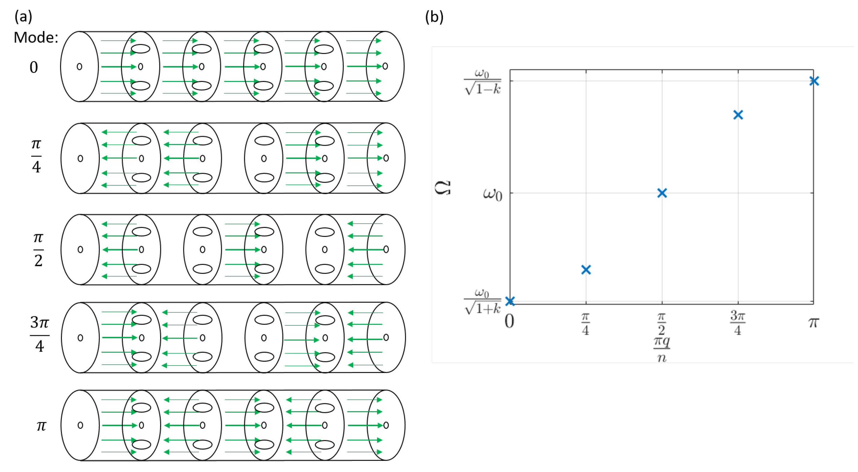
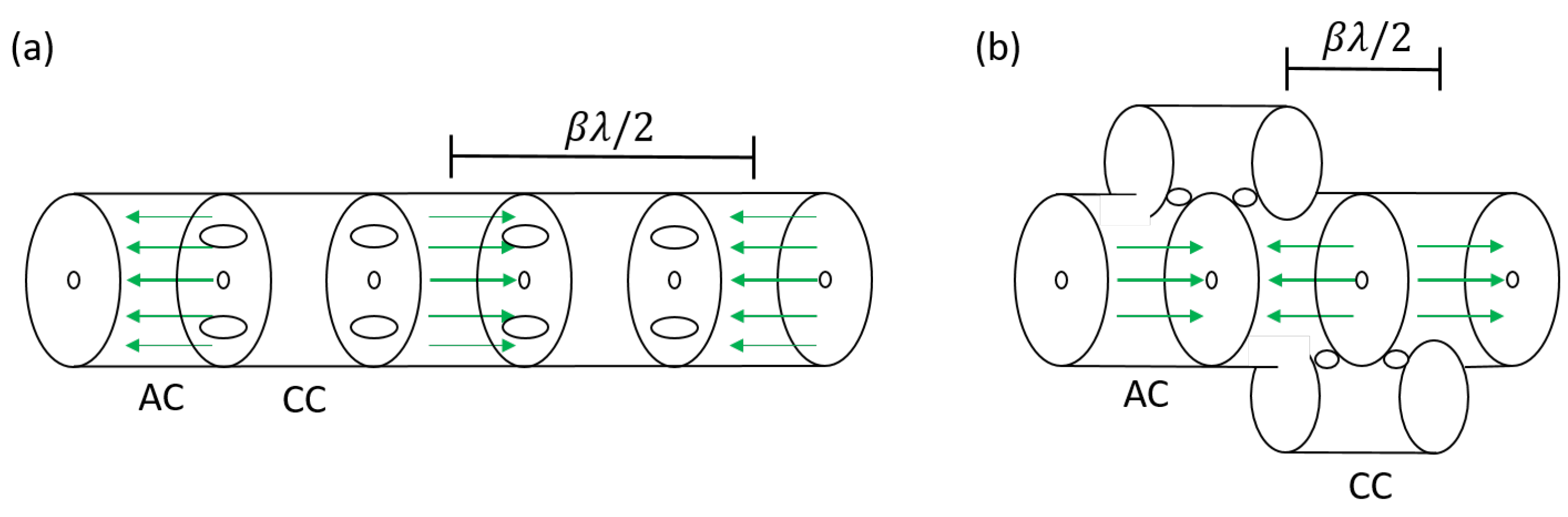
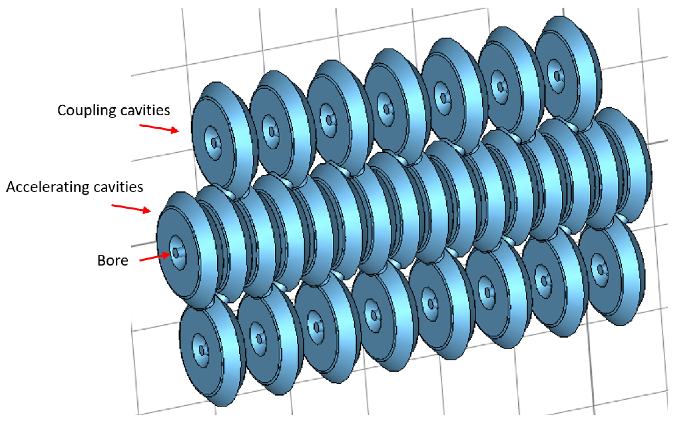
2. Principle of a Side-Coupled Cavity Linac

We briefly summarize the basic principle of a biperiodic side-coupled linac structure (SCCL) to introduce our object of study and a few figures of merit. The energy gain of a particle passing through N c single cavities is given in first order by [1]:
Δ W = q N c L c Z T 2 P cos ϕ .
Here, L c refers to the length of the single cavities, Z T 2 to the effective shunt impedance per unit length, P to the RF power consumption of the whole multi-cell structure, ϕ to a stable accelerator phase, and q to the particle’s charge. Since Δ W is proportional to N c for a given P, accelerators are usually composed of many SCs [5]. In order to reduce RF equipment and losses, SCs are usually coupled to multi-cell structures. A simple multi-cell structure is a periodic on-axis coupled structure consisting of N c = 5 T M 010 pillbox SCs, shown, for example, in Figure 2. If the SCs are tuned to each other, a number of q modes with the corresponding eigenfrequencies
Ω q = ω 0 1 + k cos ( π q / n )
are possible in the multi-cell structure. Here, ω 0 represents the resonant frequency of the SCs, k is the coupling factor, and q is { 0 , 1 , , n } , while n corresponds to N c 1 . The quantity π q n describes the phase shift per SC. Figure 2a shows the distribution of the electric field in the five-cell structure for the corresponding five modes. The correlation between the eigenfrequencies and the phase shift per SC is shown by the dispersion curve in Figure 2b.
Keeping k constant, the frequency distance δ Ω Ω of the modes becomes increasingly smaller as the number of SCs rises. Since the π 2 mode has the largest frequency distance to its neighbor modes, it is often favored for multi-cell structures for the sake of operational stability [1].
Continuous acceleration of a particle requires its synchronism with the phase of the π 2 mode; therefore, the distance between two excited cells must be β λ 2 (see Figure 3a) with β = v p c 0 , λ = c 0 f R with v p the particle velocity, c 0 the speed of light, and f R the frequency of the RF signal. However, since every second cell does not contribute to the acceleration of the particle in a periodic on-axis structure, it is not possible to achieve a high effective shunt impedance per unit of length Z T 2 (see Figure 3a). A solution to this problem is the SCCL (see Figure 3b). It consists of accelerator cells (ACs), which are optimized for a maximum Z T 2 and (in the π 2 case) field-free coupling cells (CCs), which are designed to be as compact as possible. Therefore, by moving the field-free cells away from the beam axis, the effective shunt impedance can be doubled in comparison to the on-axis coupled structure.
Since the SCCL combines the frequency stability of the π 2 mode with the high Z T 2 of the π mode, it is one of the most widely used multi-cell structures. It is used for acceleration of electrons as well as ions at velocities of β { 0.3 , 1 } in a wide variety of accelerator facilities with different operating frequencies ( f R ) as shown, e.g., in [1,25,26,27,28].

3. Materials and Methods

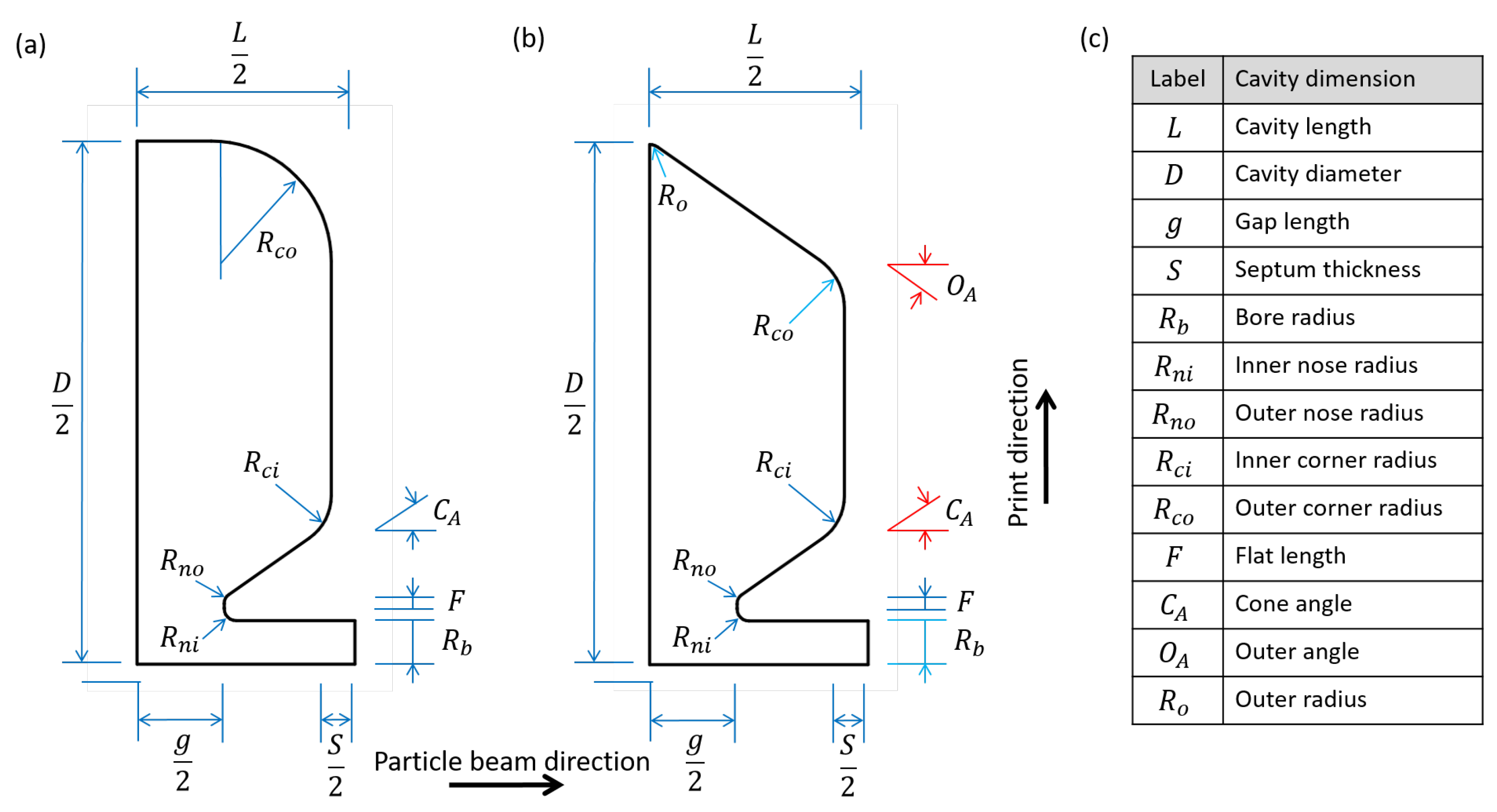
3.1. Cavity Design and Electromagnetic (EM) Simulation

A quadrant of the longitudinal section through a typical rudimentary geometry of a single accelerator cell of an SCCL structure is shown in Figure 4a. It should be noted, however, that it is only referred to as “typical” because it reflects the standard cell geometry for CCL structures in the widely used Poisson Superfish cavity design software. There are smaller or larger geometry deviations in practice. In the case of a printing direction parallel to the beam axis, either the left or the right cone would show downskin angles, α < < 45 , which would require support structures to preserve print quality. Therefore, only a printing direction perpendicular to the beam axis can be considered. As shown in Figure 4b, our rudimentary design can be manufactured with L-PBF without support structures. To be self-supporting perpendicular to the beam axis, angle O A is introduced to avoid overhangs on the cavity shell. The radii R o and R c o are introduced to obtain a continuous contour.
The angles C A and O A are crucial for the performance of an SCCL (see Section 4.1). Therefore, in this work, we evaluate five different single-cavity geometries that differ only in the angles O a and C a , corresponding to 25 , 30 , 35 , 40 , and 45 for the individual cavities, to test which minimum downskin angle can be accepted. To reduce printing effort, the diameter D of the cells was reduced to 46.5 mm ( f R > 3 GHz), and the length L of the cells was set to 19 mm ( β p r o t o n 0.38 in π 2 mode) for the evaluation. This corresponds to a proton energy of about 75 MeV in the SCCL case. To keep the gap length g and D constant, the f R of the five cavities was not optimized to a specific value. Table 1 summarizes the geometric parameters of the five single cavities.
It should be mentioned that a detailed optimization of the cavity geometries does not take place in the presented work since, for example, the geometry of the nose cone varies strongly depending on the cavity dimension and on other parameters such as the RF pulse duration. However, except for the modifications necessary for printing, the geometry of the presented single cavities is comparable to single cavities used as part of 3 GHz SCCL structures in linac-based proton therapy systems [25,28]. Some parameters, such as R n o , R n i , F, and R b , are identical.
All electromagnetic (EM) simulations for this work were performed using the eigenmode solver or frequency domain solver of the 3D EM analysis tool CST Microwave Studio® [29]. In terms of material, we always assume the annealed copper included in CST with an electrical conductivity of 5.8 × 10 7 S m (International Annealed Copper Standard, IACS).

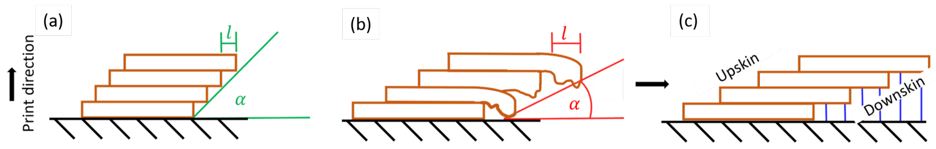
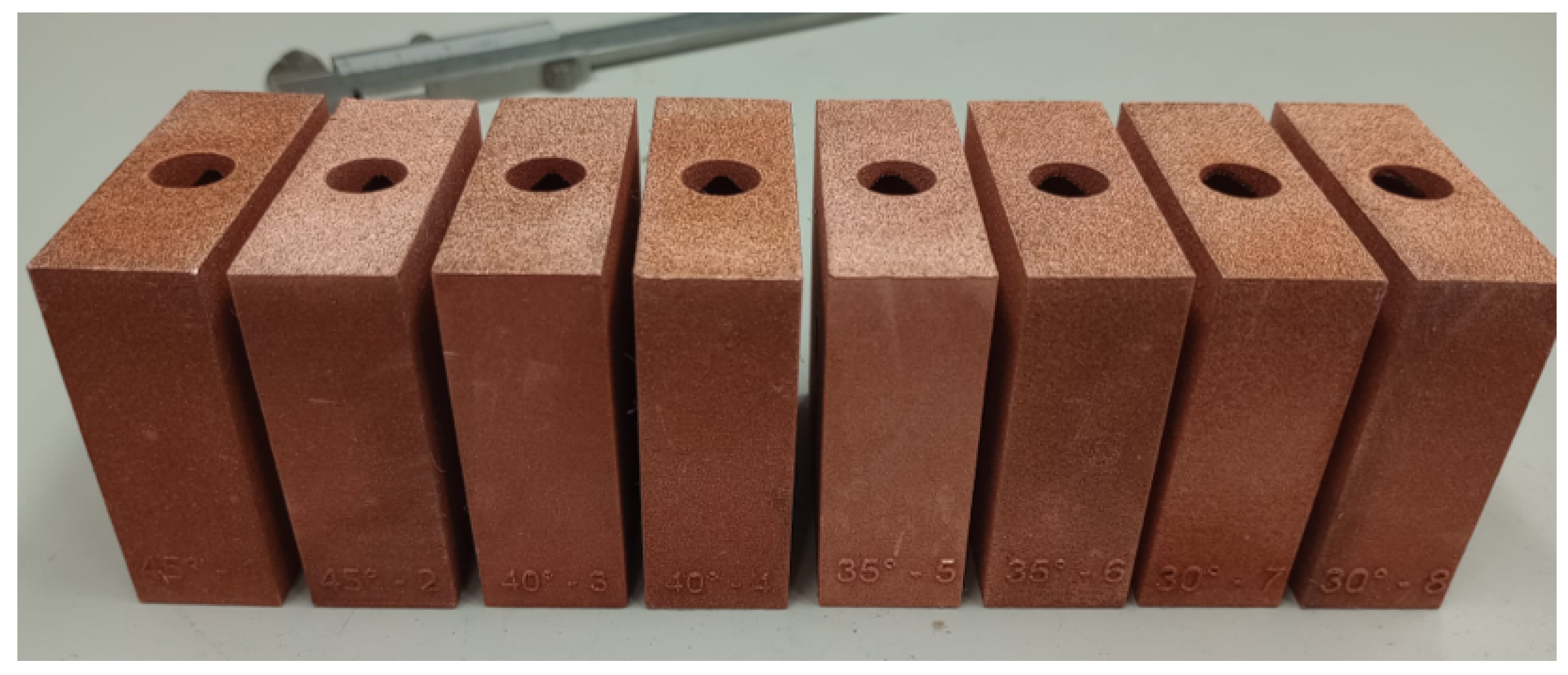
3.2. Additive Manufacturing

In order to study the effect of different C A and O A on the geometric accuracy and the surface roughness, two SC sets were printed, each with the respective angles C A / O A of 30 , 35 , 40 , and 45 . A TruPrint1000 Green Edition equipped with green laser ( λ = 515 nm) was used to print the SCs. The beam spot diameter at the laser focus point measures 210 µm. The pre-set pure copper manufacturing technological parameters and algorithms were used for the manufacturing process. The utilized process parameters are those investigated by Gruber et al. [22], which have demonstrated relative densities exceeding 99.9% and electrical conductivity surpassing 100% IACS for pure copper on the same machine. We used PureCu gas-atomized spherical-shaped copper powder from the company m4p as raw material. The chemical composition of the powder is Cu (99.95%), Ag (<0.01%), Bi (<0.01%), Pb (<0.01%), O (0.023%), and a residue (0.01%). The grain size distribution corresponds to d 10 = 19 µm, d 50 = 26 µm, and d 90 = 36 µm.

3.3. Post-Processing Procedure

In order to reduce the surface roughness and thus increase Q 0 , various processes have been proposed and tested in the past for the post-processing of printed cavities [12,20]. Due to our positive results in previous studies [20], we concentrate in this paper on the process of Hirtisation (R) developed by RENA GmbH [24]. Hirtisation (R) is a combination of different chemical/electrochemical processes. In contrast to, e.g., Chemical Mechanical Planarization (CMP) or processes using the abrasive fluidic medium, there are no mechanical processes included. In our case, the chemical process media Cu-Auxilex (R) and Cu-Delevatex (R) were used. Four Hirtisation (R) cycles were performed on cavity set 2. The first three cycles aimed for a material removal ( M R ) of 70 µm, while the last cycles aimed for M R = 140 µm. Whether the desired M R was achieved was evaluated by comparing the cell length L before and after each cycle. One 70 µm cycle lasted approximately 30 min. During the process, the SCs are completely immersed in the process bath. The orientation of the SCs corresponds to the orientation during printing. The gas bubbles resulting from the chemical processes can therefore easily escape through the holes provided for the coupling and pickup loop (see holes in Figure 5a).

3.4. RF Measurements

In this work, the resonant frequency f R and the unloaded quality factor Q 0 of the cavities are evaluated. f R is measured to draw conclusions about the geometric manufacturing accuracy and thus to assess the frequency range in which cavities can be manufactured using AM (see Section 3.5). The unloaded quality factor Q 0 = ω W P of a cavity compares the power loss P per RF cycle with frequency 2 π f = ω in the cavity walls with the energy W stored in the cavity. Therefore, Q 0 describes the ability of the cavity to store energy and thus the potentially achievable E-field strength in the cavity. f R and Q-factor Q 0 were determined using a Siglent SNA5012A vector network analyzer (VNA) and a coupling loop probe (CLP) via a reflection measurement (S11). The VNA was calibrated to the end of the CLP. All measurements refer to the T M 010 mode of the respective SCs.

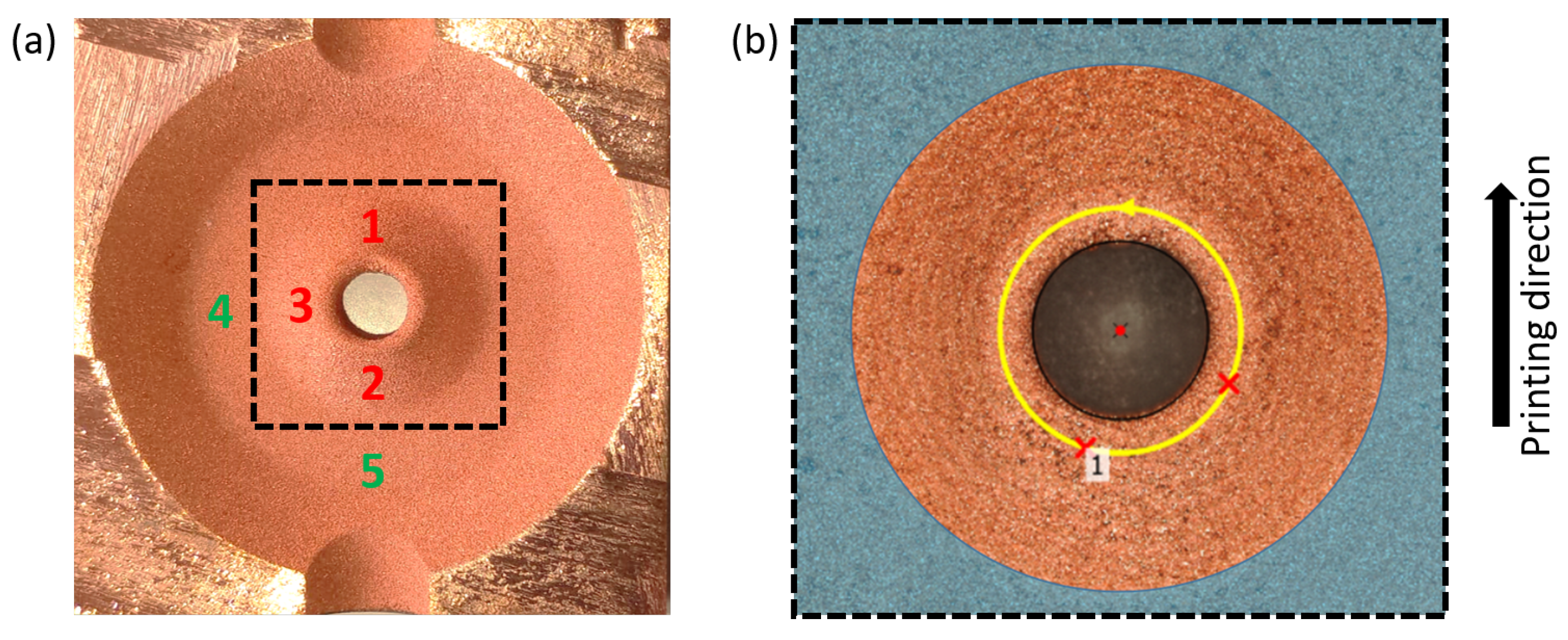
3.5. Evaluation of Dimensional Accuracy

The geometric accuracy of the SCs is assessed by three different methods.
Method 1: f R is proportional to 1 L C , where L corresponds to the inductance, and C corresponds to the capacitance of a cavity. Looking at the E-field distributions in Figure 6, it becomes clear that, e.g., the capacitance of the cavity is mostly determined by the distance and the shape of the nose cones. Since each geometrical deviation causes a change in L and C, measuring f R cannot be used to infer a deviation at a specific location in the cavity. Rather, the measurement of f R allows a statement about the absolute accuracy. By comparison with the simulated f R , a first estimation can be made whether AM can be used in the respective frequency range. Since the extent of the change of the resonance frequency Δ f R depends on the relative change of the individual dimensions, a deviation of, e.g., 20 µm of g has a greater effect on f R than the same deviation of D. Therefore, we illustrate Δ f R in the following by Δ g . This comparison is based on Δ f R Δ g = 0.21 MHz μ m simulated by CST.
Method 2: The SCs are cut into halves, which are subsequently examined with a Keyence VR-5000 wide-area 3D measurement system using the structured light method with 12× magnification and an automatic stage. The 3D data are compared with the SC CAD file, and a false color plot of the deviations Z is generated. Although the measurement accuracy of ± 4 µm with image stitching is not sufficient to evaluate small deviations, it is possible to visualize a general trend.
Method 3: To evaluate the geometric accuracy of the nose cone as the part with the highest demands on geometric accuracy, the prominence h of the nose cone tip above the cavity wall was assessed using the Keyence VR-5000 in 40× magnification mode. According to the cell design, h corresponds to h = L / 2 S / 2 g / 2 = 6 mm. h was determined as shown in Figure 5b. The cavity walls perpendicular to the beam axis (blue shaded area in Figure 5b) were used as a reference surface. The nose cone tip was found by extracting the bore center (red dot) from the scan data and creating a measurement circle (yellow) with a diameter of 8 mm. Therefore, the prominence h corresponds to the distance between the circle and the reference plane.

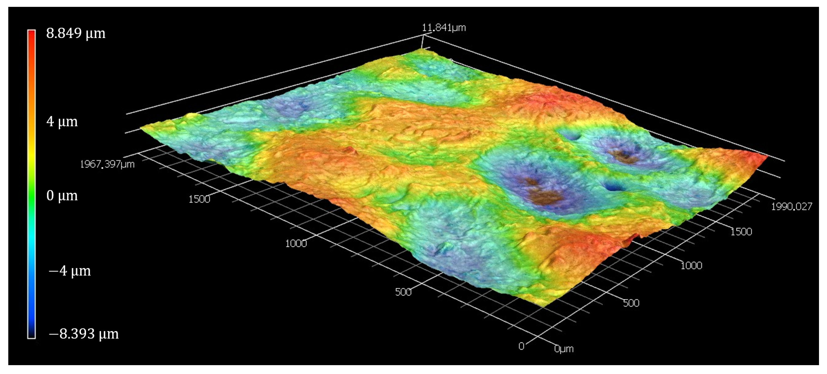
3.6. Evaluation of Surface Roughness

We characterize the surface roughness with the surface parameters of area root-mean-square average S q , adapted from ISO 25178 and S q λ , which is exactly like S q but with an additional high-pass filter.
This decision was made based on the following considerations. Q 0 is inversely proportional to the surface resistivity, which, for a smooth surface ( S q < < δ ), is given by R S 0 = 1 σ δ . Here, σ denotes the electrical conductivity (for pure copper, around 5.8 × 10 7 S m ), and δ denotes the skin depth, after which the current density drops to 1 e due to the skin effect ( δ 1.1 µm for f R = 3 GHz). The surface resistance increases with the surface roughness, which can be taken into account by a loss enhancement factor η > 1 through the relationship R S = η · R S 0 [18]. The most common models to estimate η for accelerator design are certainly phenomenological models, such as the Hammerstad model [30]. Here, the roughness of the surface is approximated by triangular parallel trenches as they appear in conventional machining. This approximation allows η to be estimated by the root-mean-square average profile height R q but fails for additive manufactured surfaces, which usually have an isotropic, Gaussian distributed roughness. Physical models such as the “Snowball” model or the Multilevel Hemispherical Model and other approaches that, for example, measure the surface using atomic force microscopy and then simulate the resistance with CST Studio, require long computation times or the precise measurement of the surface texture and are hardly applicable to complex cavity geometries. Furthermore, these models do not take into account how the internal inductance L i , which is influenced by the surface properties of the conductor, changes the surface impedance [31].
Our approach is to use the Gradient Model developed by Gold et al. [31], which describes the propagation of electromagnetic waves along rough surfaces and takes into account the influence on L i . The model shows good agreement in the simulation of printed circuit board (PCB) transmission lines up to 100 GHz, and only R q is required for its application. Since additive manufactured surfaces have an isotropic surface, it can be assumed that the roughness of a line in the first iteration corresponds to that of a surface (e.g., R q S q ). Moreover, even if the surfaces are not isotropic, it is not necessarily the case that the direction of the current flow corresponds to the measurement direction of R q . To overcome this limitation and gain statistics at the same time, we evaluate S q instead of R q .
The evaluation of the surface texture parameters is performed with the Keyence VK-X3000 laser scanning microscope. The 20× lens in the extra-long working distance version was used. As shown in Figure 5a, the roughness of the cells is determined at five locations on the cavity surface. Red and green text marks the measurement locations on the nose cone and cavity sidewall, respectively. Locations 1 and 3 represent an upskin and a downskin surface, respectively. Positions 3, 4, and 5 are located on a normal surface relative to the building platform. An area of around 4 mm 2 was evaluated at the measurement locations. The recorded surface profiles were post-processed by the functions Noise removal (level “High”) and Missing data removal. A low-pass filter ( λ s -Filter) with a wavelength λ s = 2.5 µm and a form correction operator (F-Operator) with a wavelength of λ f = 130 µm were applied.
Moreover, a high-pass filter ( λ c -Filter) with the wavelength λ c was used to remove the process specific waviness from the corrected surface. In [31], it is stated that surface variations appearing with λ > > δ can be neglected for AC impedance. Thus, we decided to define λ c as the copper powder size d 50 , to λ c = d 50 = 26 µm. S q λ is therefore determined between the wavelength limits λ s and λ c (S-L surface).

4. Results

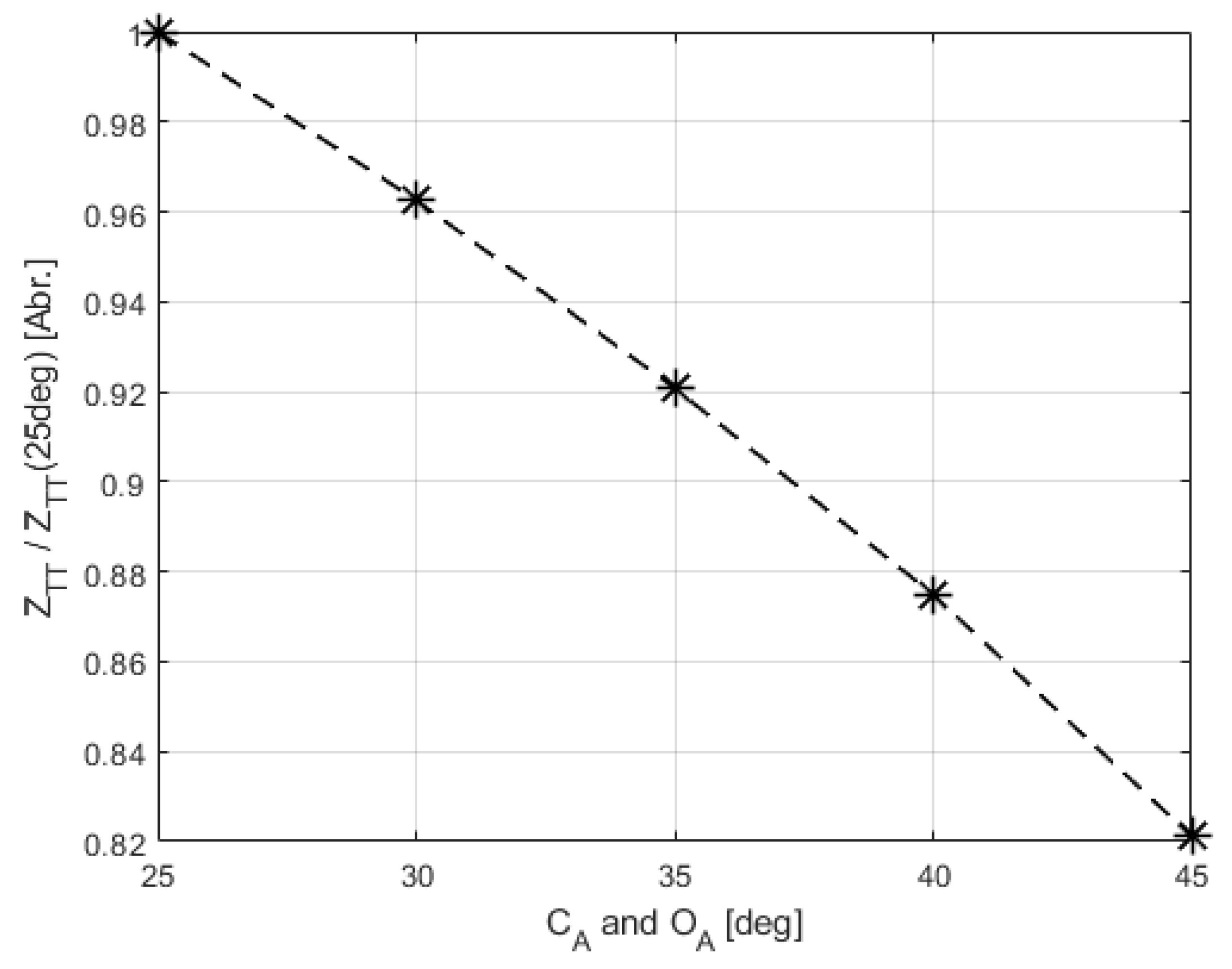
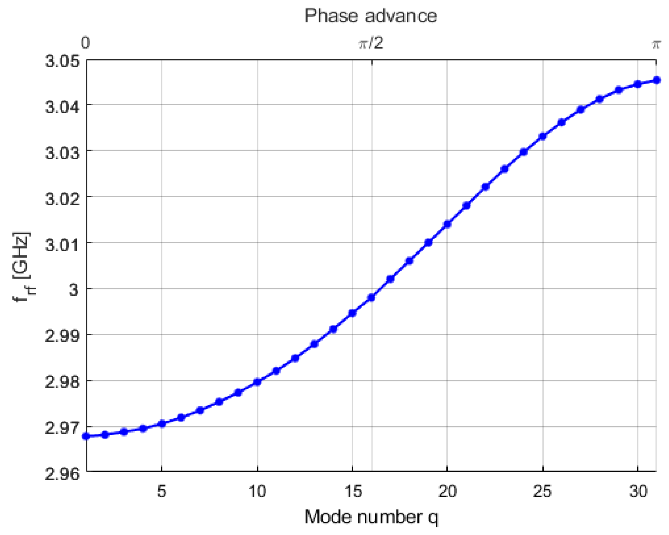
4.1. Single-Cell EM Simulations

In the following, we evaluate how the RF characteristics of the single cavities for L-PBF depend on the angles O A and C A . The distribution of the electric (E) and magnetic (B) fields in the longitudinal section is shown in Figure 6 for the (a) 25 and (b) 45 single cavity.
For linac-based proton therapy systems, a breakdown rate (BDR) of 10 6 bpp m is targeted. The unit bpp/m indicates the number of breakdown events (b) per RF pulse (pp), normalized to one meter (m) of cavity structure. To predict the high-gradient performance and thus the BDR, the quantities E m a x E 0 , H m a x E 0 , and S c , m a x E 0 can be analyzed. Here E m a x and H m a x denote the maximum E- and H-field in the cavity, E 0 the average acceleration gradient, and S c , m a x the maximum value of the modified Poynting vector S c = R e { S } + g c · I m { S } . The weighting factor g c is considered to be 0.2 [32,33]. To realize this BDR in cavities at an RF pulse length of 2.5 µs (flattop) and resonance frequencies < 5 GHz , E m a x E 0 < 4.63 , H m a x E 0 < 2.80 A kV , and S c , m a x E 0 < 0.63 A kV are mandatory [34]. Table 2 summarizes the key RF parameters of the five single cavities studied. All cavities would achieve the desired BDR.
Figure 7 shows the effective shunt impedance per length Z T 2 normalized to the Z T 2 of the 25° SC as a function of C A and O A , respectively. It can be seen that the normalized Z T 2 decreases for increasing angles C A and O A . For example, if C A and thus O A are increased from 25 to 45 , the normalized Z T 2 is reduced by about 18%.

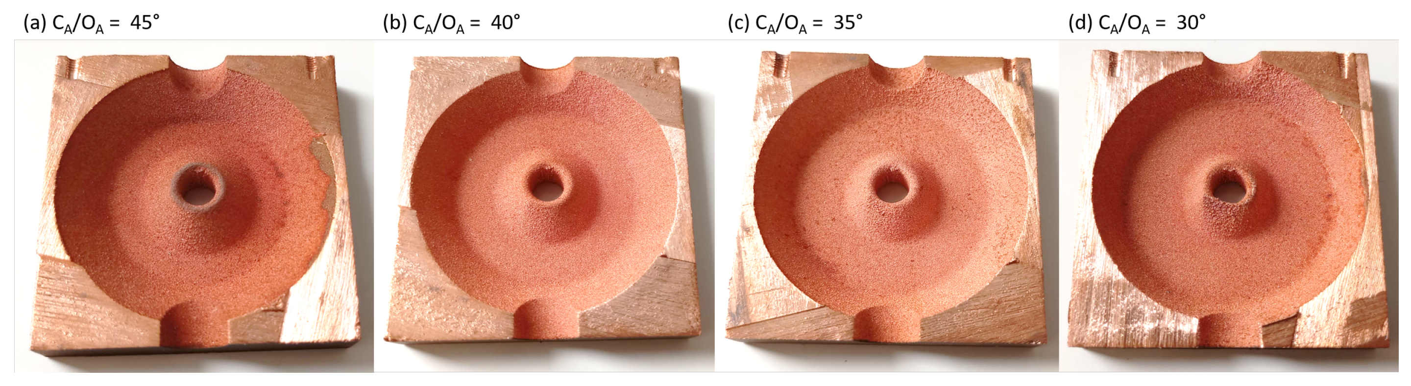
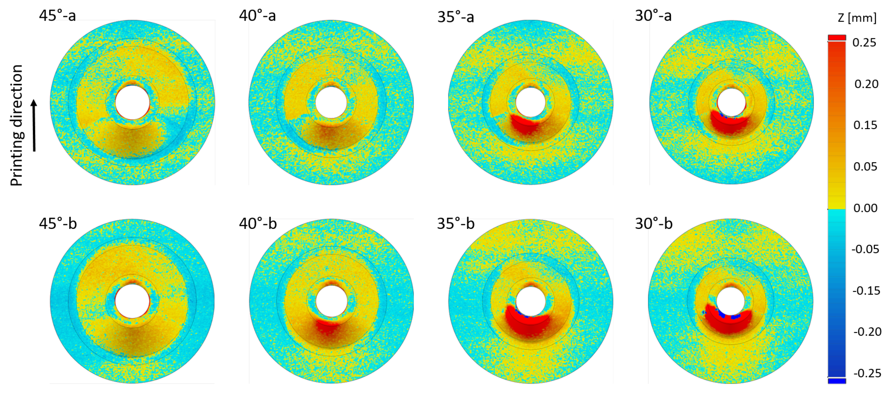
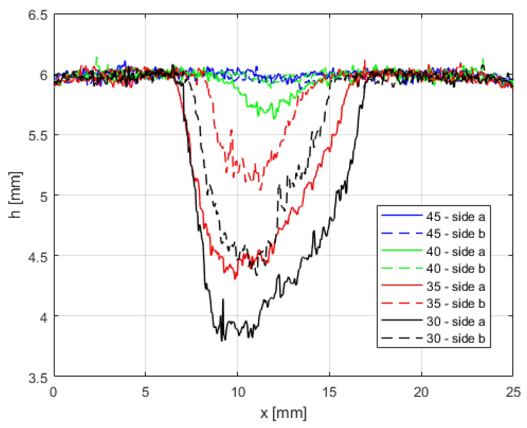
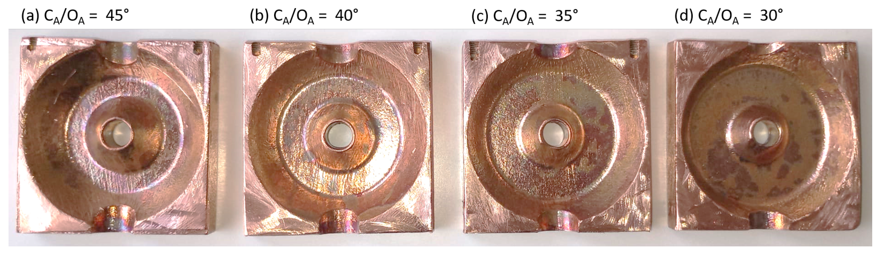
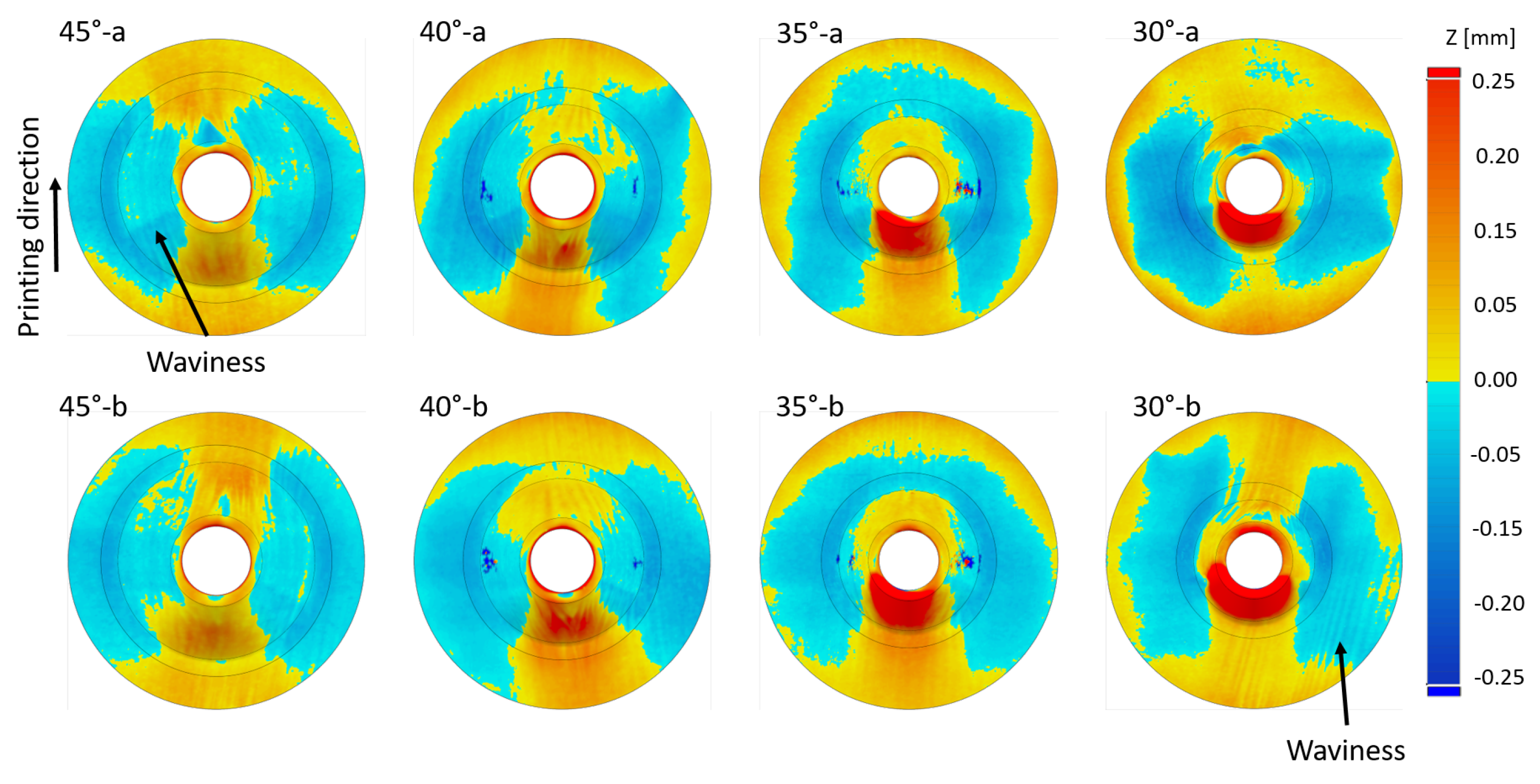
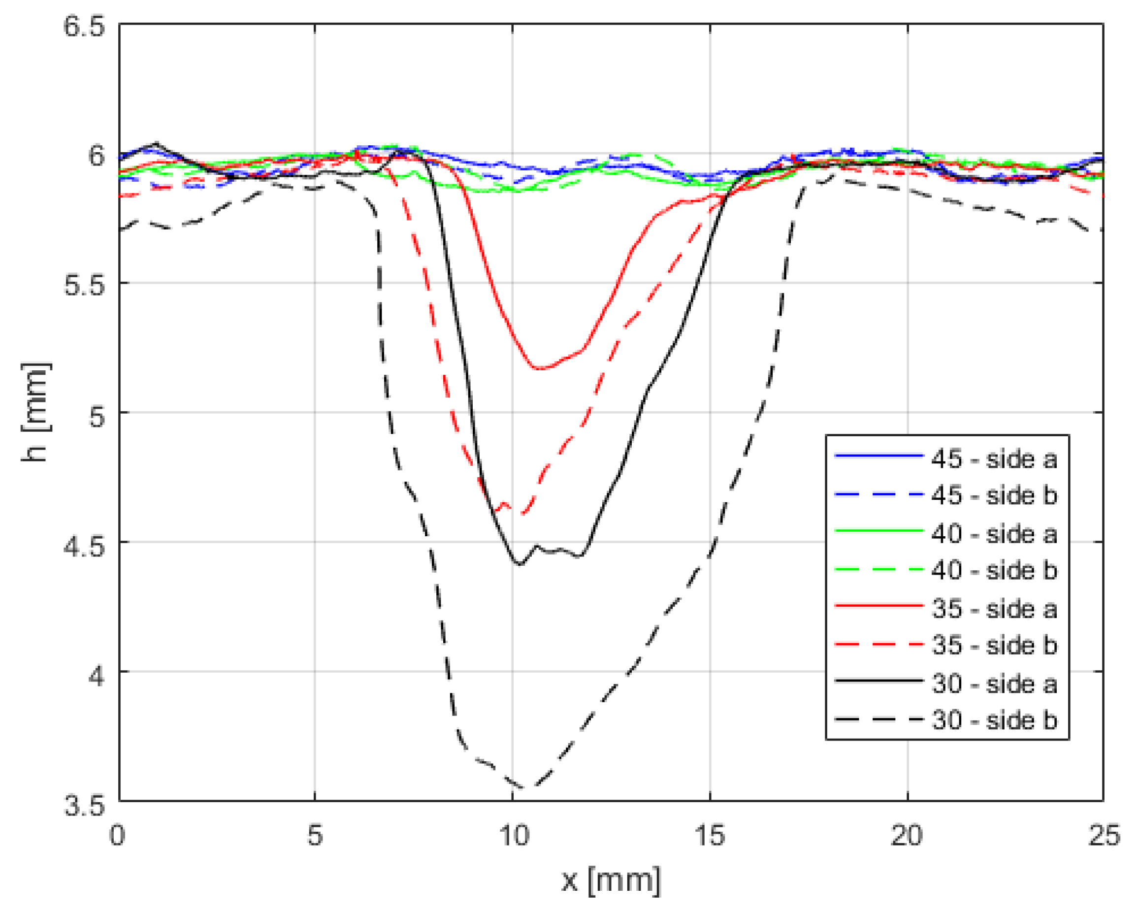
4.2. Dimensional Accuracy after Printing

In this section, we evaluate which angles C A and O A (see Figure 4) can be realized and how they affect geometrical accuracy. Figure 8 shows the two manufactured cell sets of the respective angles C A and O A of 30 , 35 , 40 , and 45 . Due to strong defects and deformations on the downskin surfaces, the structure with C A = O A = 25 could not be manufactured, which is why it was excluded from further study. The holes on the top side of the struts, which are also found on the bottom side, are intended for the insertion of the RF coupling loop probes.
Figure 9 illustrates the f R analysis of the individual additively manufactured SCs. The deviations Δ f R of the measured f R from the f R simulated by CST are indicated by circles (blue) and triangles (green) for the first set and second set of SCs, respectively. The values marked with an asterisk (black) correspond to the Δ f R between the two SC sets. The values marked with a cross (red) represent the maximum frequency tuning achievable with conventional tuning devices, as used in proton therapy linac SCCL structures. These values were scaled from an analysis of the tuning characteristics of 3 GHz SCCL cells [34]. From a geometric perspective, a Δ f R of 4.2 MHz corresponds to a gap length g deviation of about 20 µm for an f R of 4 GHz. In the case of a SCCL, all SCs must be tuned to a certain resonant frequency to produce a continuous dispersion relation. For this, the geometrical deviations of all cells must lie within the possible tuning range. As can be seen in Figure 9, this requirement is only fulfilled with C A = O A = 45 .
In order to evaluate the achieved manufacturing accuracy in more detail, set 1 of the SCs was cut to open the structures. Figure 10 shows one half of each cut SC. In particular, the 30 SC shows significant deformation and “drop formation” on the downskin faces.
Figure 11 shows the height deviation Z between CAD data and the surface data measured with the Keyence VL-700 optical 3D scanner of both halves of the cut-open cell. The geometric accuracy decreases with decreasing angles of C A and O A . For C A = O A < 35 , a Z of >0.25 mm results for large regions on the downskin surface of the nose. Only for C A = O A = 45 is an accuracy of ≈±0.05 mm achieved over almost the entire geometry. The geometry of the aperture, although printed without a support structure, shows virtually no deformation. This is because small radii of curvature in the range of a few millimeters can be considered to be self-supporting.
The measured prominence h of the nose cone is shown in Figure 12 for both sides of the cut SC set 1. The x-coordinate represents the length of the circle path, where x = 0 corresponds to the yellow arrow at “12 o’clock” on the yellow circle in Figure 5b. As expected, the dominant deviations from the planned h = 6 mm can be found for all cells at the nose cone’s downskin surface with respect to the printing direction (see printing direction in Figure 5a). Figure 11 and Figure 12 indicate that the b-side of the cells seems to have more serious deviations than the a-side.
Table 3 shows the average prominence h and the deviation from the planned g. For a C A = O A = 45 , a g of 4.02 mm results. The deviation from the planned g corresponds to a Δ f R of about 4.2 MHz, which is just within the tunable range. We therefore conclude that the 45 cells can be printed with the accuracy required for SCCL structures with an f R < 4 GHz.

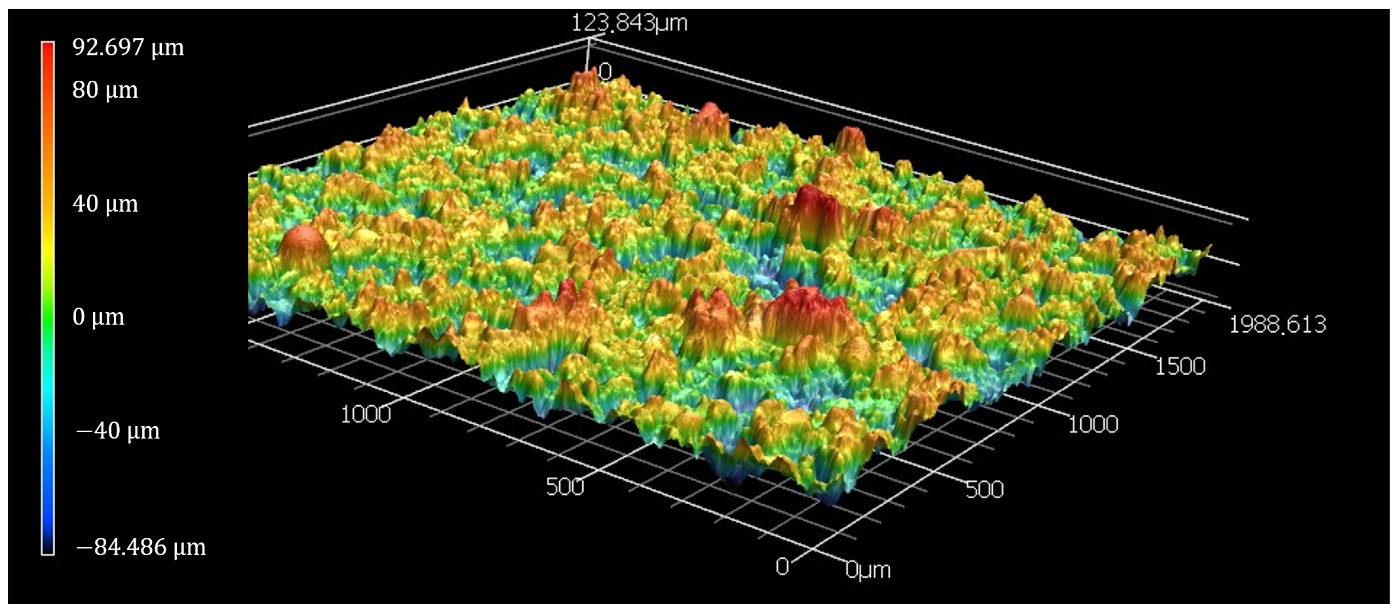
4.3. Surface Roughness after Printing

As demonstrated with previous cavity prototypes, the L-PBF process results in a surface roughness of S q > 10 µm, which greatly reduces the measured vs. simulated Q 0 ( Q 0 M and Q 0 S , respectively) [19]. The measured S q and S q λ at locations 1–5 are shown in Table 4. Roughly, S q ranges from 18 µm to 30 µm, and S q λ ranges from 3 µm to 6 µm for all SCs. S q and S q λ are practically identical for all locations in the case of the 45 SC. There are also no remarkable differences between the individual SCs. This is mainly due to the applied F-Operator and λ c -Filter. These define geometric inaccuracies such as those found on the downskin of the nose cone, in particular the 30 SC, as waviness instead of roughness.
Figure 13 shows the measured surface at location 4. The high surface roughness results mainly from incompletely melted powder grains that form the outermost layer of all non-treated work pieces manufactured by means of L-PBF.

4.4. Dimensional Accuracy after Post-Processing

Figure 14 shows the cut SCs of set 2 after finishing (Hirtisation (R)). Compared with the SCs after printing (Figure 10), the surface of the structures appears much smoother and shinier. Figure 15 shows a comparison of the CAD data with the measured surface data Z of the two halves of the set 2 SCs. As with the set 1 SCs, the geometric accuracy decreases with decreasing angles of C A and O A , respectively, and a maximum deviation on the order of + 0.25 mm is seen at the nose cone in the case of C A = O A < 40 . However, compared to set 1, even the SC with C A = O A = 45 does not show a uniform geometry (material removal). Instead, all SCs show a waviness perpendicular to the printing direction and irregularities below and above the nose cone, as marked for SC half 45 a and 30 b . The orientation of the SCs during Hirtisation (R) corresponds to the printing direction to ensure that the gas generated during Hirtisation (R) escapes through the CLP holes. Therefore, the trenches of the waviness and the irregularities most likely result from the ascent behavior and paths of the gas bubbles and the associated reduction of material removal on the inner surfaces of the SCs.
The measured prominence h of the nose cone is shown in Figure 16 for both sides of the cut SCs of set 2. The dominant deviations from the planned h = 6 mm can again be found at the nose cone’s downskin surface, concerning the printing direction. As with the untreated SCs (compare Figure 11 and Figure 12), the b-side of the cells appears to have more significant degradation, reinforcing the suspicion of asymmetry in the printing process.
Table 5 shows the average prominence h. For a C A and O A of 45 , a g of 4.110 ± 0.083 mm results. The deviation from the planned g corresponds to an Δ f R of about 16 MHz. However, it is likely that more material was removed at the tips of the nose cone geometry by the Hirtisation (R) process than at the cavity wall due to their prominence.
Figure 17 shows the resulting f R shift relative to f R after printing the SCs as a function of the material removal M R . For the first 70 µm of M R (1st Hirtisation (R) cycle), the change in resonant frequency is >40 MHz for all cells. The following cycles influence the resonance frequency less. In the L-PBF process, there is always a transition area between completely melted material and powder that has not been completely melted. The contour of a printed component therefore always offers a large interaction surface (see Figure 13). The large initial effect of cycle 1 is therefore probably because this first layer can be removed very efficiently compared with dense material. The substantial deviation of the 30 SC from the others after the first cycle can probably be explained by the fact that small downskin angles C A and O A generally result in many irregularities, which also offer a large interaction surface for Hirtisation (R). However, Δ f R also increasingly differs between 35 , 40 , and 45 SCs starting from M R = 70 µm. After M R = 350 µm, Δ f of, e.g., 45 and 35 SCs differs by 13 MHz, which could not be corralled by tuning devices anymore. All SCs were treated together in the same Hirtisation (R) process. Therefore, further optimization is needed for the post-processing approach.

4.5. Q 0 and Surface Roughness after Post-Processing

The purpose of post-processing the SCs is to minimize the surface roughness and thus maximize Q 0 .
The measured S q and S q λ at locations 1–5 after Hirtisation (R) are shown in Table 6. S q ranges from 1 µm to 2 µm for all samples and locations. S q λ ranges from 0.2 µm to 0.4 µm. Again, the roughness S q and S q λ are practically identical for all cells with different C A and O A . However, the S q λ measured on the nose cone (Loc. 1–3) are higher than on the cavity wall (Loc. 4 and 5).
Figure 18 shows an example of the measured surface at location 4. Compared to the untreated surface shown in Figure 13, the post-processed sample is clearly smoother and shows no extreme peaks or powder adhesions. Note that the dimension of the color scale of Figure 13 is a factor of 10 larger than the color scale of Figure 18.
Figure 19 shows the measured quality factor ( Q 0 M ) normalized to the quality factor simulated by CST ( Q 0 S ) as a function of the material removal M R for the different SCs of set 2. To allow a geometry-independent comparison, the void volume of each SC was increased by the respective M R in all directions for the simulation of Q 0 S . The Q 0 M Q 0 S of the SCs obtained in the individual steps from printing to Hirtisation (R) step 4 is almost identical. By removing 140 µm of material, it was possible to increase Q 0 M from between 20–25% to 72–75% of the simulated value Q 0 S . The subsequent two Hirtisation (R) steps (up to M R = 350 µm) show no further effect on Q 0 M .
In black, Figure 20 shows Q 0 S as a function of the cavity surface roughness S q λ predicted by the gradient model. The prediction by the Hammerstad model [30] is shown in blue. The simulations were performed using CST Microwave Studio [31]. The single measurement points indicate the Q 0 M / Q 0 S values of the SCs with C A = O A of 30 , 35 , 40 , and 45 . Additionally, the values after additive manufacturing (set 1) and after maximum material removal M R = 350 µm (set 2) are marked by points and crosses, respectively. Before Hirtisation (R), the Q 0 M / Q 0 S of all SCs are consistent with the model within the measurement error. The Q 0 M / Q 0 S after Hirtisation (R) do not match the gradient model, except for the 30 SC. The mean values of Q 0 M / Q 0 S after Hirtisation (R) are reduced by about 8% to 18% compared to the gradient model. Since the skin depth δ varies with the frequency, the predictions of the two models also vary for the different SCs. However, this variation is negligible compared to the size of the plotted points, which is why only one line is shown for each of the two models.

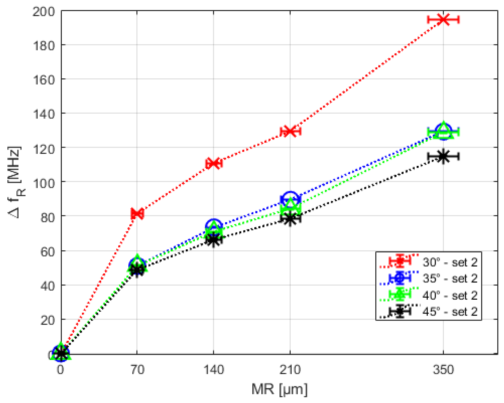
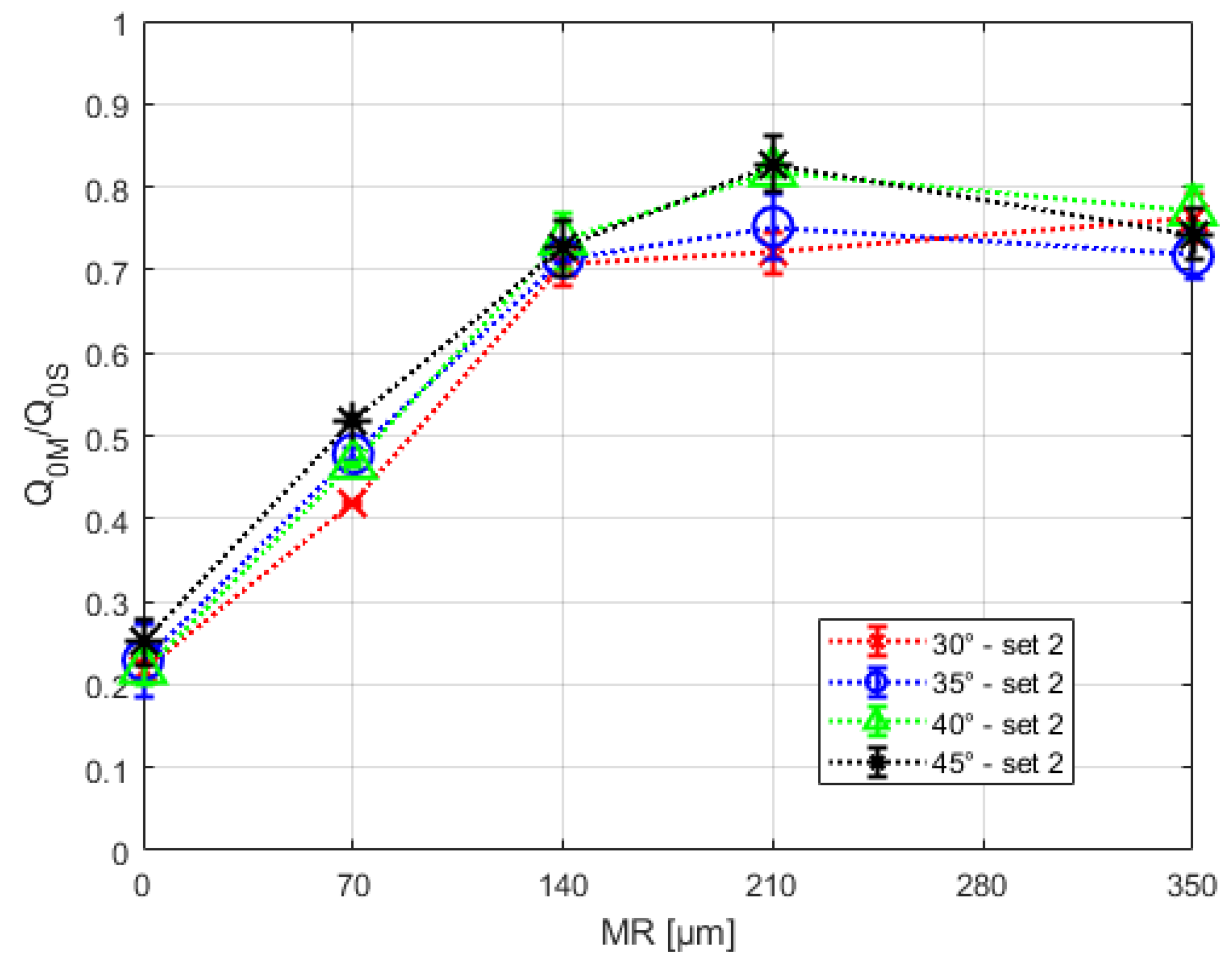
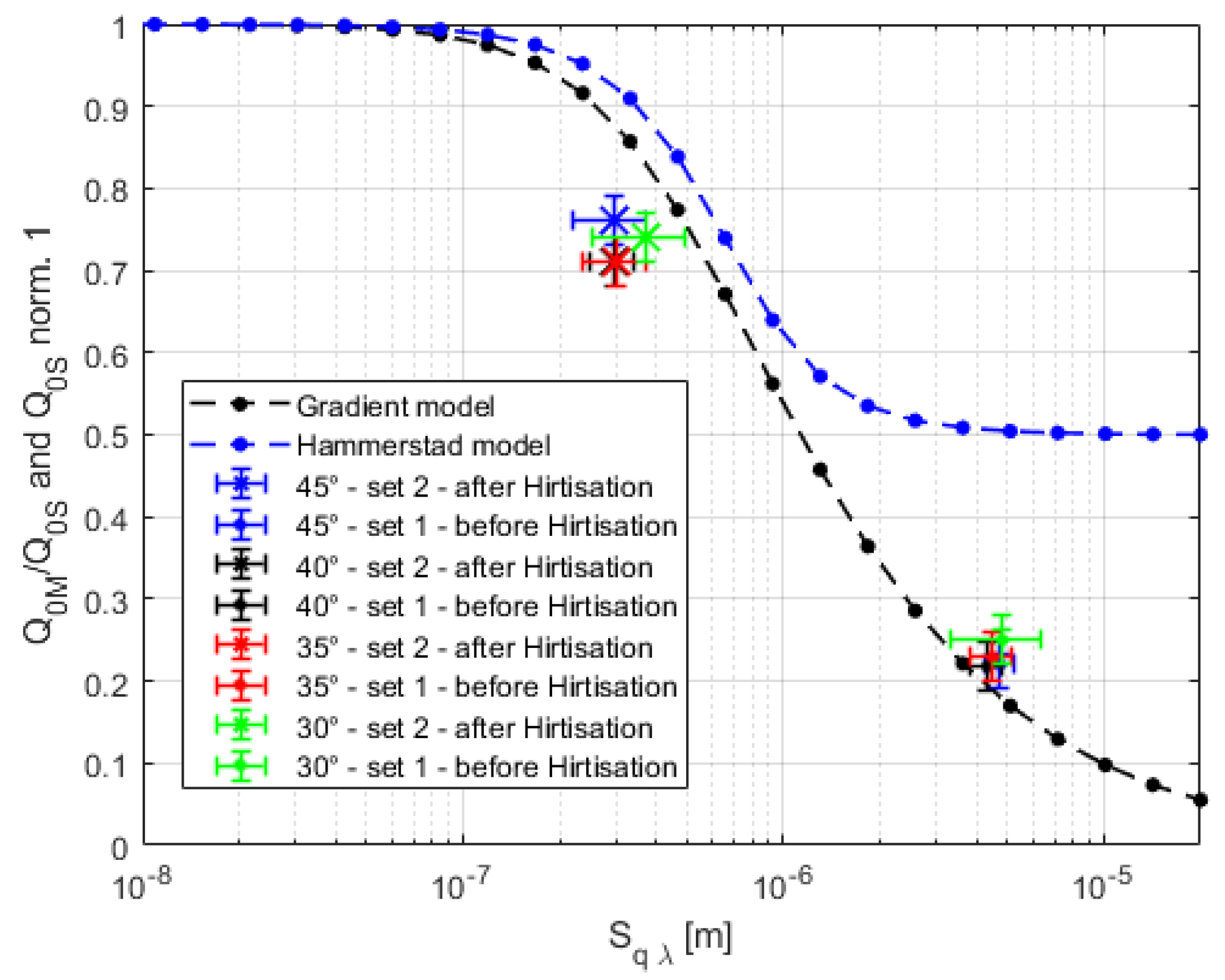
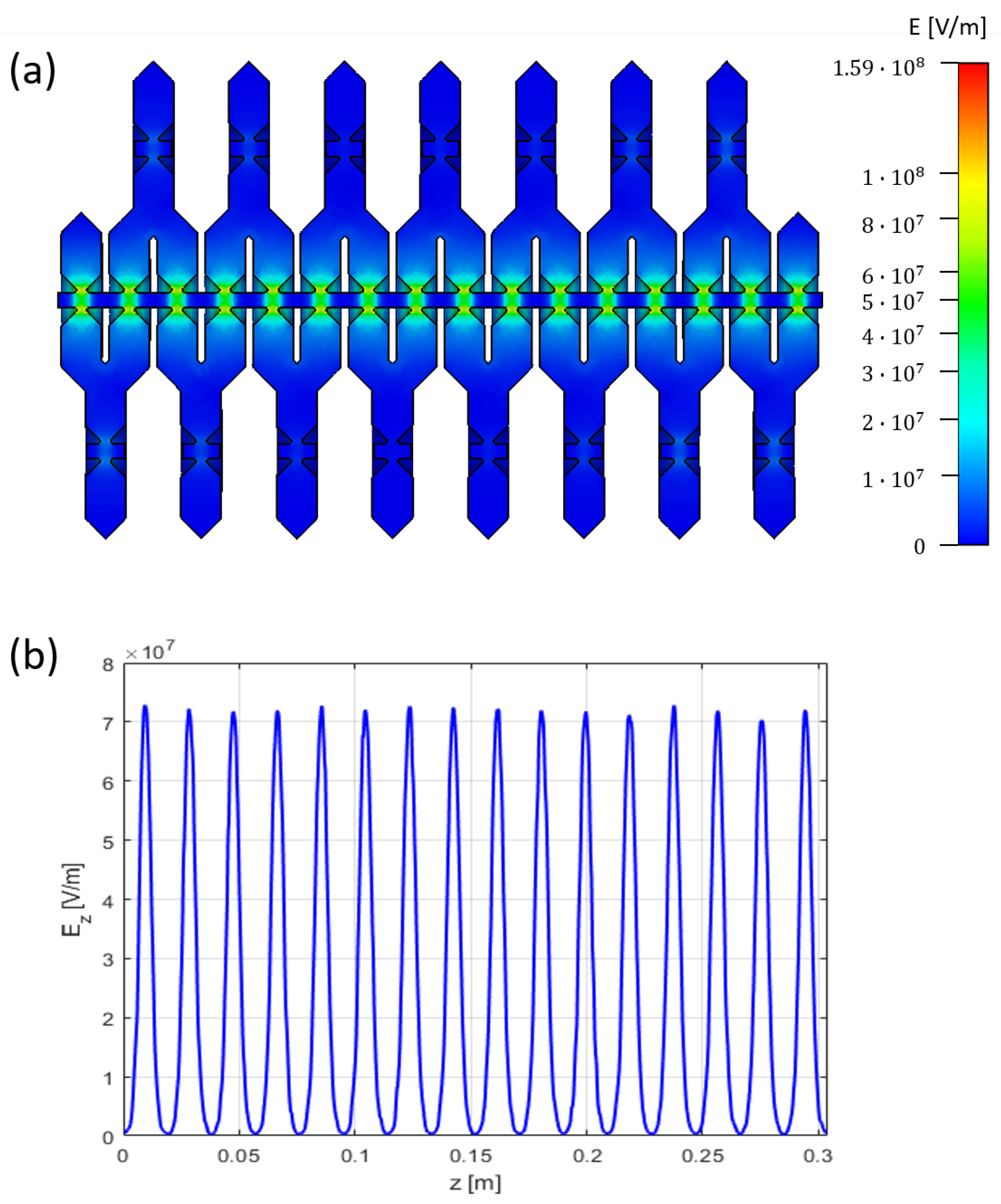
4.6. Self-Supporting 3 GHz Biperiodic Side-Coupled Linac Concept
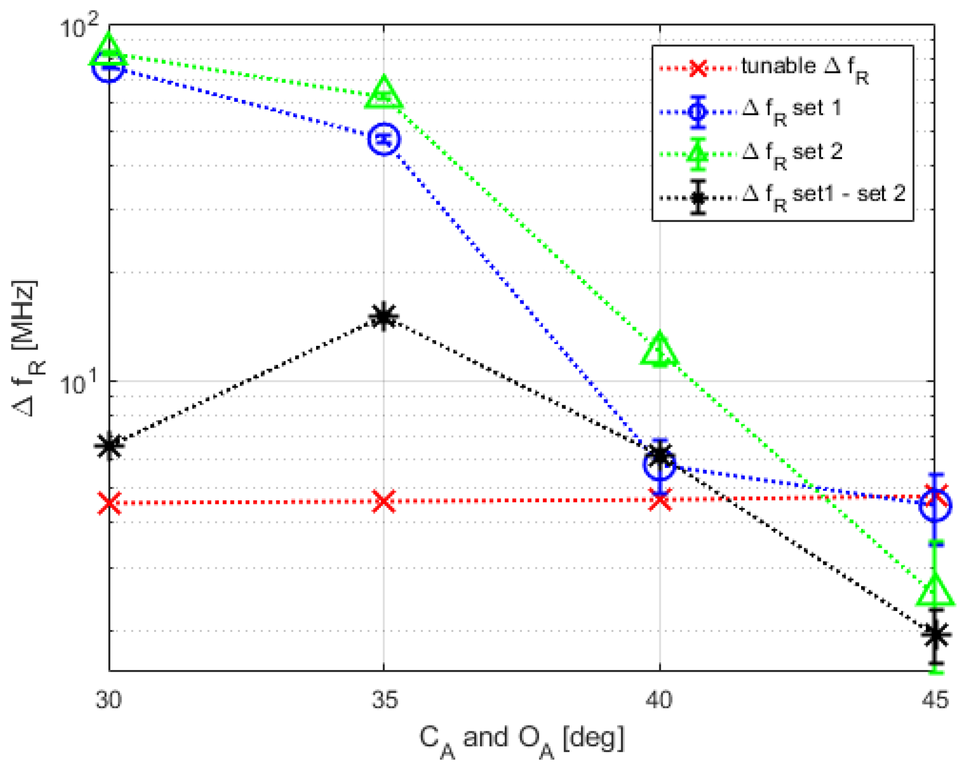
In this section, a rudimentary, self-supporting 3 GHz biperiodic side-coupled linac concept (SCCL concept) is presented and evaluated by simulations. The concept is comparable to the 3 GHz CCL modules used in proton therapy linac facilities. Figure 21 shows the vacuum volume of the 304 mm long SCCL concept, consisting of 16 ACs and 15 CCs.
To achieve a self-supporting structure, the ACs and CCs are shaped comparably to the self-supporting single cavities developed in the previous sections. Figure 22 shows the unit cell of the CAD file as used for the CST simulations in (a) perspective, (b) a section of the perspective, (c) the half CC side, and (d) the half AC side. Due to the high manufacturing accuracy, an angle of C A = O A = 45 was preferred. The cell diameter D was increased to 69.5 mm to increase f R roughly to 3 GHz. The final frequency tuning of the accelerator and coupling cavities is done by varying the gap length g. All other geometrical parameters are adopted from the developed self-supporting single cavities (see Table 2). Therefore, the SCCL concept is designed for accelerating protons with an initial energy of about 75 MeV in π 2 mode.
Using CST Microwave Studio, the g of the individual cells was optimized to reach the π 2 mode at f R 2998 MHz, resulting in the dispersion curve shown in Figure 23.
The optimized gap lengths of the CCs and ACs are approximately 4.289 mm and 4.158 mm, respectively. Exceptions to this are the two outermost ACs, whose gap length corresponds to approximately 4.062 mm. This is because the two outermost ACs are each coupled to only one CC instead of two as the other ACs are. The coupling aperture corresponds to an ellipse with a length of its major axis of 12 mm. The coupling aperture is located symmetrically to AC and CC in the unit cell, resulting in a minor axis length of 6.68 mm. The coupling coefficient obtained by the coupling aperture corresponds to approximately k = f R ( π ) f R ( 0 ) f R ( π / 2 ) = 2.5% (cf. Figure 23). The E-field distribution of the π 2 mode in the whole SCCL concept is shown in Figure 24a. Figure 24b shows the E-field distribution on the beam axis, with the maxima of the field distribution across the gaps of each AC.

5. Discussion

In this work, our previously presented approach for designing cavities that can be manufactured using additive manufacturing techniques is used to develop a first concept of a biperiodic side-coupled linac (SCCL). Basic single cavities (SCs) with different downskin angles ( C A and O A ) were simulated by CST and manufactured from pure copper using green laser L-PBF to evaluate this approach. The main achievements are as follows.
The normalized Z T 2 decreases with increasing downskin angles ( C A and O A ). An increase from 25 to 45 corresponds to a reduction in Z T 2 by about 18%. Small angles should therefore be preferred (see Section 4.1).
The TruPrint1000 Green Edition enables additive manufacturing of SCs with C A = O A > 35 . However, only the SC with C A = O A = 45 achieves the geometric accuracy required for frequency tuning, with an f R > 3 GHz. This is especially evident by comparing the measured and simulated f R of the cells (compare Section 4.2). Through optical measurements of the nose cone height and a CAD geometry comparison on the cut SCs, it can be seen that the downskin surface of the nose cone geometry in particular becomes less stable with decreasing C A and O A . Nevertheless, in theory, the geometric deviations remain constant for all geometry sizes using L-PBF. With decreasing f R , however, higher geometrical deviations can be accepted, which probably allows for AM of larger cavities, even with smaller angles.
In addition to S q (ISO 25178), the quantity S q λ was introduced to evaluate the SCs’ surface roughness (see Section 3.6). Compared to S q , an additional high-pass filter ( λ c -Filter) was applied, with λ c = 26 µm for S q λ . This corresponds to the mean powder diameter ( d 50 ). The measured S q λ of the SCs after printing is in the range of 3 µm to 6 µm.
To minimize surface roughness and thus maximize Q 0 , the second set of SCs was post-processed by four Hirtisation (R) steps, removing approximately a total of 350 µm of material. The SCs show a wavy pattern after Hirtisation (R) (see Figure 14). The trenches of this wave pattern most likely result from the rising of gas bubbles during Hirtisation (R). However, Figure 17 shows that Hirtisation (R) makes it possible to tune the resonance frequency of a single cell. Over the last cycle, the resonant frequency shifts by about 0.21 MHz μ m in the case of the 45 cell, and a one-minute process time results in 2.3 µm of material removal. Therefore, it can be assumed that the resonance frequency can be set more accurately than 1 MHz using an iterative Hirtisation (R) approach. It remains to be investigated whether the same amount of material is removed by Hirtisation (R) for all SCs in an SCCL. Compared to the roughness after printing, S q and S q λ are reduced by a factor of 15–20 by Hirtisation (R) (compare Table 4).
Figure 19 shows that, for the cavities manufactured, Q 0 S could not be achieved by Hirtisation (R). After removing 140 µm of material, Q 0 M was increased from 20–25% to 72–75% of Q 0 S . Further material removal of up to M R = 350 µm could not further increase Q 0 M . The Q 0 M of all SCs obtained in the individual steps from printing to Hirtisation (R) step 4 are almost identical. The print quality of the downskin surface of, e.g., the 30 SC and the 45 SC differs significantly, however, which becomes obvious, e.g., for the downskin of the nose cone in the 30 case. This implies that the assumption that long wavelength variations of the surface ( λ > > δ ) do not influence the RF conductivity is correct and that the form correction of the surface for determining surface roughness has at least no negative influence.
The comparison between the measured Q 0 M and the Q 0 S predicted by the gradient model shows a broad agreement before Hirtisation (R) (see Figure 20). This can be seen as a first strong indication that the combination of the gradient model and our filter approach to characterize the surface roughness ( S q λ ) could allow a straightforward prediction of Q 0 M from simple AM samples by measuring S q λ . However, compared to the prediction from the gradient model, the mean values of Q 0 M after Hirtisation (R) are reduced by about 8–18% (see Figure 20). This could, for example, indicate that the filter settings for the measurement of the surface roughness are not yet optimal or that impurities such as hydrogen, hydrocarbon, or carbon deposition during Hirtisation (R) reduce Q 0 M . It is also possible that the conductivity of the material after Hirtisation (R) only reaches the conductivity of IACS after a baking procedure.
If the gradient model is assumed to be valid, a Q 0 greater than 95% of the achievable Q 0 (according to CST simulations) is only possible for an S q λ of less than 100 nm. At least for the SC presented here, this roughness level could not be achieved by means of Hirtisation (R). Whether the manufacturing process can be further optimized must be evaluated in further studies. Additional post-processing processes, such as MMP Technology (R), may also be applied.
Based on the SC findings, a basic self-supporting 3 GHz biperiodic side-coupled linac concept was developed in Section 4.6. The SCCL concept is designed for accelerating protons with an initial energy of about 75 MeV in π 2 mode. Due to the manufacturing accuracy required for an f R of 3 GHz, the 16 ACs and 15 CCs are based on the C A = O A = 45 SC (see Figure 21). However, the SCCL concept is not fully optimized. Rather, it is a first study to evaluate whether AM enables the fabrication of an SCCL structure. Requirements for beam current, accelerator voltage, breakdown rate, etc. have a significant influence on the geometry of the nose cone (including the bore hole, etc.) and therefore on the effective accelerating voltage. Therefore, a final optimization of the geometry to maximize the effective shunt impedance Z T 2 to produce efficient and compact accelerator systems is only reasonable if a specific application is in focus. Moreover, ACs and CCs are assumed to be identical. For example, the EM field in the CCs can be further optimized by optimizing the nose cones in the CCs. In addition, the transverse dimensions of the SCCL concept can certainly be reduced in the future by reducing the transverse CC dimension compared to the AC dimension, as is the case in most conventional SCCL systems.
Nevertheless, a rudimentary comparison with the 3 GHz SCCL modules used in proton therapy linac facilities underlines the potential of the SCCL concept. The Z T 2 simulated by CST corresponds to 60.13 M Ω m for a transit time factor of T = 0.881 (75 MeV protons). With an input power of 1 MW (peak), the 304 mm long SCCL concept would increase the proton energy by about 4.2 MeV. This corresponds to the same performance of comparable, traditionally manufactured SCCL modules [28,35]. Nevertheless, it should be noted that T was calculated for a particle energy of 75 MeV. When passing through the structure, the particle gains energy ( Δ W ), which leads to a slight decrease in T and thus Z T 2 , if the cell length (L) remains constant. However, the AM process allows each cell to be manufactured with an optimal cell length in terms of particle energy without additional cost or effort. Although this can also be done in traditional manufacturing, it is often avoided for cost reasons, as (small) series production of the individual parts of the single cavities becomes practically impossible.
Like Q 0 M , Z T 2 would be reduced by about 18% compared to the simulation after Hirtisation (R) (see Figure 19). This results in a 10% decrease in Δ W . To achieve the same particle energy, accelerator structures manufactured according to the approach presented here would have to be longer and/or supplied with more input power. However, as we showed in previous studies, AM has the potential to reduce cavity manufacturing costs by up to 70% [19]. Since cavity structures are responsible for a large part of the investment costs of accelerator facilities, the reduced performance could potentially be compensated by the significant reduction in manufacturing costs in many cases.

Outlook

The manufacturing approach of the L-PBF process in combination with electrochemical post-processing will be further optimized. Figure 11 and Figure 12 indicate that the b-side of the single cavities seems to have more serious deviations than the a-side. This indicates a systematic asymmetry in the L-PBF process, which should be investigated in more detail.
The effect of Hirtisation (R) on geometry and material properties needs to be analyzed in more detail. The waviness caused by Hirtisation (R) (see Figure 14) is most likely due to rising gas bubbles on the cavity walls. Furthermore, the measurements of h indicate that uniform material removal is not guaranteed (compare Figure 15 and Figure 17). Both effects are significantly influenced by the flow and rising direction of the process liquids and gas bubbles and may be minimized by rotating (moving) the geometry during the process. How and whether this is possible remain to be investigated.
Moreover, we plan to perform studies to further validate the gradient model and improve the roughness filter settings. In addition, the impact of bake-out processes on Q 0 will be investigated.
High power RF tests (high gradient tests) are the most important outstanding studies from the perspective of the intended usage in high-performance linacs. For this reason, we are also currently constructing a high-gradient test bench based on a 3 GHz magnetron–modulator combination. In preparation for the tests, we are planning to investigate how wave guides and vacuum flanges can be attached to AM cavities. Earlier prototypes have already shown that threads can be cut in AM copper that allow flanges to be attached directly to the cavity using an O-ring seal. A pressure of 2 × 10 7 mbar was achieved, which is perhaps already sufficient [19,36].
Finally, the first SCCL multi-cell structures will be printed soon to determine how the achieved manufacturing accuracy affects the coupling between the individual ACs and CCs.

Author Contributions

Conceptualization, M.M. and G.D.; methodology, M.M., G.G., S.B. and S.G.; software, M.M., R.H. and G.G.; validation, M.M., G.G. and R.H.; formal analysis, M.M. and S.B.; investigation, M.M.; resources, G.D., S.B., E.L. and L.S.; data curation, M.M.; writing—original draft preparation, M.M. and G.D.; writing—review and editing, M.M., G.D., G.G., S.B., S.G., R.H., E.L. and L.S.; visualization, M.M. and S.B.; supervision, G.D.; project administration, M.M.; funding acquisition, G.D. All authors have read and agreed to the published version of the manuscript.

Funding

The study is partly funded by the Federal Ministry of Education and Research (BMBF) via ERUM-Pro and the EU project Radiate. In addition, the equipment used in this study from the FLAB-3Dprint research project is funded by dtec.bw-Forschungszentrum Digitalisierung und Technik der Bundeswehr, for which we would like to express our sincere thanks. dtec.bw is funded by the European Union-NextGenerationEU.

Data Availability Statement

The data presented in this study are available on request from the corresponding author.

Conflicts of Interest

The authors declare no conflict of interest.

References

  1. Wangler, T.P. RF Linear Accelerators, 2nd ed.; John Wiley & Sons: Hoboken, NJ, USA, 2008; pp. 98–121. [Google Scholar]
  2. Kutsaev, S.V. Advanced technologies for applied particle accelerators and examples of their use. Tech. Phys. 2021, 66, 161–195. [Google Scholar] [CrossRef]
  3. Lung, H.M.; Cheng, Y.C.; Chang, Y.H.; Huang, H.W.; Yang, B.B.; Wang, C.Y. Microbial decontamination of food by electron beam irradiation. Trends Food Sci. Technol. 2015, 44, 66–78. [Google Scholar] [CrossRef]
  4. Do Huh, H.; Kim, S. History of radiation therapy technology. Korean Soc. Med. Phys. 2020, 31, 124–134. [Google Scholar]
  5. Amaldi, H.; Braccini, S.; Puggioni, P. High frequency linacs for hadrontherapy. Rev. Accel. Sci. Technol. 2009, 2, 111–131. [Google Scholar] [CrossRef]
  6. Witman, S. Ten Things You Might Not Know about Particle Accelerators. Available online: https://www.symmetrymagazine.org/article/april-2014/ten-things-you-might-not-know-about-particle-accelerators?language_content_entity=und (accessed on 1 November 2023).
  7. Wilson, I.H. Cavity construction techniques. In Proceedings of the CERN Accelerator School of RF Engineering for Particle Accelerators, Oxford, UK, 3–10 April 1991; Volume 2. [Google Scholar] [CrossRef]
  8. Nassiri, A.; Chase, B.; Craievich, P.; Fabris, A.; Frischholz, H.; Jacob, J.; Jensen, E.; Jensen, M.; Kustom, R.; Pasquinelli, R.; et al. History and technology developments of radio frequency (RF) systems for particle accelerators. IEEE Trans. Nucl. Sci. Inst. Electr. Electron. Eng. 2016, 63, 707–750. [Google Scholar] [CrossRef]
  9. Ghodke, S.R.; Barnwal, R.; Mondal, J.; Dhavle, A.S.; Parashar, S.; Kumar, M.; Nayak, S.; Jayaprakash, D.; Sharma, V.; Acharya, S.; et al. Machining and brazing of accelerating RF cavity. In Proceedings of the 2014 International Symposium on Discharges and Electrical Insulation in Vacuum (ISDEIV), Mumbai, India, 28 September–3 October 2014; pp. 101–104. [Google Scholar]
  10. Calignano, F.; Manfredi, D.; Ambrosio, E.P.; Biamino, S.; Lombardi, M.; Atzeni, E.; Minetola, P.; Iuliano, L.; Fino, P. Overview on Additive Manufacturing Technologies. IEEE Inst. Electr. Electron. Eng. 2017, 105, 101–104. [Google Scholar] [CrossRef]
  11. Attaran, M. The rise of 3-D printing: The advantages of additive manufacturing over traditional manufacturing. Bus. Horizons 2017, 60, 677–688. [Google Scholar] [CrossRef]
  12. Torims, T.; Cherif, A.; Delerue, N.; Pedretti, M.F.; Krogere, D.; Otto, T.; Lopez, E.; Otto, T.; Pikurs, G.; Pozzi, M.; et al. Evaluation of geometrical precision and surface roughness quality for the additively manufactured radio frequency quadrupole prototype. J. Phys. Conf. Ser. 2023, 2420, 012089. [Google Scholar] [CrossRef]
  13. Torims, T.; Pikurs, G.; Gruber, S.; Vretenar, M.; Ratkus, A.; Vedani, M.; López, E.; Brückner, F. First proof-of-concept prototype of an additive manufactured radio frequency quadrupole. Instruments 2021, 5, 35. [Google Scholar] [CrossRef]
  14. Hähnel, H. Update on the first 3D printed IH-type linac structure-proof-of-concept for additive manufacturing of linac RF cavities. In Proceedings of the 31st Linear Accelerator Conference, Liverpool, UK, 28 August–2 September 2022; Volume 22, pp. 170–173. [Google Scholar]
  15. Hähnel, H.; Ateş, A.; Dedić, B.; Ratzinger, U. Additive Manufacturing of an IH-Type Linac Structure from Stainless Steel and Pure Copper. Instruments 2023, 7, 22. [Google Scholar] [CrossRef]
  16. Frigola, P.; Agustsson, R.B.; Faillace, L.; Murokh, A.Y.; Ciovati, G.; Clemens, W.A.; Dhakal, P.; Marhauser, F.; Rimmer, R.; Spradlin, J.; et al. Advance Additive Manufacturing Method for SRF Cavities of Various Geometries; Thomas Jefferson National Accelerator Facility (TJNAF): Newport News, VA, USA, 2015. [Google Scholar]
  17. Creedon, D.L.; Goryachev, M.; Kostylev, N.; Sercombe, T.B.; Tobar, M.E. A 3D printed superconducting aluminium microwave cavity. Appl. Phys. Lett. 2016, 109, 032601. [Google Scholar] [CrossRef]
  18. Riensche, A.; Carriere, P.; Smoqi, Z.; Menendez, A.; Frigola, P.; Kutsaev, S.; Araujo, A.; Matavalam, N.G.; Rao, P. Application of hybrid laser powder bed fusion additive manufacturing to microwave radio frequency quarter wave cavity resonators. Int. J. Adv. Manuf. Technol. 2023, 124, 619–632. [Google Scholar] [CrossRef]
  19. Mayerhofer, M.; Mitteneder, J.; Dollinger, G.; Mayerhofer, M. A 3D printed pure copper drift tube linac prototype. Rev. Sci. Instrum. 2022, 93, 023304. [Google Scholar] [CrossRef] [PubMed]
  20. Mayerhofer, M.; Mittenender, J.; Wittig, C.; Prestes, I.; Jägle, E.; Dollinger, G. First High Quality Drift Tube Linac Cavity additively Manufactured from Pure Copper. In Proceedings of the 14th International Particle Accelerator Conference (IPAC23), Venicem, Italy, 7–12 May 2023; Volume 143. [Google Scholar]
  21. Tran, T.Q.; Chinnappan, A.; Lee, J.K.Y.; Loc, N.H.; Tran, L.T.; Wang, G.; Kumar, V.V.; Jayathilaka, W.A.D.M.; Ji, D.; Doddamani, M.; et al. 3D printing of highly pure copper. Metals 2019, 9, 756. [Google Scholar] [CrossRef]
  22. Gruber, S.; Stepien, L.; López, E.; Brueckner, F.; Leyens, C. Physical and geometrical properties of additively manufactured pure copper samples using a green laser source. Materials 2021, 14, 3642. [Google Scholar] [CrossRef] [PubMed]
  23. Mayerhofer, M.; Dollinger, G. Manufacturing Method for Radio-Frequency Cavity Resonators and Corresponding Resonator. Patent EP3944725A1, US20230300969A1, 23 July 2020. [Google Scholar]
  24. Rena Technologies GmbH. Surface Treatment of 3D-Printed Metal Parts. 2023. Available online: https://www.rena.com/en/technology/process-technology/hirtisation (accessed on 1 November 2023).
  25. Ronsivalle, C.; Picardi, L.; Ampollini, A.; Bazzano, G.; Marracino, F.; Nenzi, P.; Snels, C.; Surrenti, V.; Vadrucci, M.; Ambrosini, F. First acceleration of a proton beam in a Side Coupled Drift tube Linac. Europhys. Lett. 2015, 111, 14002. [Google Scholar] [CrossRef]
  26. Aubin, S.T.; Steciw, S.; Fallone, B.G. The design of a simulated in-line side-coupled 6 MV linear accelerator waveguide. Med. Phys. 2010, 37, 466–476. [Google Scholar] [CrossRef]
  27. Tantawi, S.; Nasr, M.; Li, Z.; Limborg, C.; Borchard, P. Design and demonstration of a distributed-coupling linear accelerator structure. Phys. Rev. Accel. Beams 2020, 23, 092001. [Google Scholar] [CrossRef]
  28. Degiovanni, A.; Stabile, P.; Ungaro, D.; SA, A. LIGHT: A linear accelerator for proton therapy. In Proceedings of the NAPAC2016, Chicago, IL, USA, 9–14 October 2016; Volume 32. [Google Scholar]
  29. Dassault Systèmes; CST Microwave Studio. 2023. Available online: https://www.3ds.com/de/produkte-und-services/simulia/produkte/cst-studio-suite/ (accessed on 1 November 2023).
  30. Hammerstad, E.; Jensen, O. Accurate models for microstrip computer-aided design. In Proceedings of the 1980 IEEE MTT-S International Microwave Symposium Digest, Washington, DC, USA, 28–30 May 1980; pp. 407–409. [Google Scholar]
  31. Gold, G. A Physical Surface Roughness Model and Its Applications. IEEE Trans. Microw. Theory Tech. Inst. Electr. Electron. Eng. 2017, 65, 3720–3732. [Google Scholar] [CrossRef]
  32. Grudiev, A.; Calatroni, S.; Wuensch, W. New local field quantity describing the high gradient limit of accelerating structures. Phys. Rev. Spec. Top.-Accel. Beams 2009, 12, 102001. [Google Scholar] [CrossRef]
  33. Benedetti, S.; Amaldi, U.; Degiovanni, A.; Grudiev, A.; Wuensch, W. RF design of a novel S-band backward traveling wave linac for proton therapy. In Proceedings of the LINAC2014, Geneva, Switzerland, 31 August–5 September 2014. [Google Scholar]
  34. Degiovanni, A. High Gradient Proton Linacs for Medical Applications. Ph.D. Thesis, École Polytechnique Fédérale de Lausanne, Lausanne, Switzerland, 2014. [Google Scholar]
  35. Ronsivalle, C.; Carpanese, M.; Marino, C.; Messina, G.; Picardi, L.; Sandri, S.; Basile, E.; Caccia, B.; Castelluccio, D.M.; Cisbani, E. The Top-Implart Project. Eur. Phys. J. Plus 2011, 126, 1–15. [Google Scholar] [CrossRef]
  36. Igarashi, Y.; Yamaguchi, S.; Higashi, Y.; Enomoto, A.; Oogoe, T.; Kakihara, K.; Ohsawa, S. High-gradient Tests on an S-band Accelerating Structure. In Proceedings of the 21st International Linac Conference, Gyeongju, Republic of Korea, 19–23 August 2002. [Google Scholar]
Figure 1. Illustration of four printed layers (brown) forming an overhang with an angle α between it and the building platform (black). (a) A large α allows for high-quality prints. (b) Layer deformation increases as α decreases. (c) Support structures (blue) are needed to ensure print quality with a small α .
Instruments 07 00056 g001
Figure 2. (a) Periodic on-axis coupled structure of five SCs with the five specific modes. In green, the E-field distribution of the modes is displayed. (b) Dispersion relation between eigenfrequencies and phase shift per SC.
Instruments 07 00056 g002
Figure 3. (a) Periodic on-axis coupled structure in π 2 mode. (b) Side-coupled cavity structure (SCCL) in which the field-free cells were removed from the beam axis, thus increasing the effective shunt impedance per unit of length Z T 2 .
Instruments 07 00056 g003
Figure 4. Quadrant of the longitudinal section through an AC of an SCCL structure as (a) traditional geometry and (b) L-PBF optimized geometry. Table (c) summarizes the relevant geometric parameters.
Instruments 07 00056 g004
Figure 5. (a) Positions for S q measurement on the nose cone (red) and on the side wall of the cavity (green). (b) Measurement principle for h.
Instruments 07 00056 g005
Figure 6. Distribution of electric (E) and magnetic (B) fields in the longitudinal section of the (a) 25 and (b) 45 single cavity.
Instruments 07 00056 g006
Figure 7. Z T 2 normalized to the Z T 2 of the 25° SC as a function of C A or O A .
Instruments 07 00056 g007
Figure 8. Cell pairs of the respective angles C A and O A of 30 , 35 , 40 , and 45 .
Instruments 07 00056 g008
Figure 9. Circles and triangles indicate Δ f R of the measured and simulated f R for the first (blue) and second (green) SC set, respectively. The asterisks (black) correspond to the Δ f R between the two SC sets. The crosses represent the maximum possible frequency tuning.
Instruments 07 00056 g009
Figure 10. One half of each cell with the respective angles C A and O A of 30 , 35 , 40 , and 45 .
Instruments 07 00056 g010
Figure 11. Difference Z between measured surface and CAD data of the individual SC halves (halve a and halve b).
Instruments 07 00056 g011
Figure 12. The prominence h for different angles C A and O A and sides of the cut-open cells. The x-coordinates are located on the yellow circle shown in Figure 5b. x = 0 corresponds to the yellow arrow, and the measurement direction corresponds to the direction of the arrow.
Instruments 07 00056 g012
Figure 13. Surface at location 4 after printing.
Instruments 07 00056 g013
Figure 14. One half of each cell with the respective angles C A and O A of 30 , 35 , 40 , and 45 after Hirtisation (R).
Instruments 07 00056 g014
Figure 15. Difference Z between measured surface and CAD data of the individual SC halves (halve a and halve b) after Hirtisation (R).
Instruments 07 00056 g015
Figure 16. The prominence h for different angles C A / O A and sides of the cut-open SCs after Hirtisation (R). The x-coordinates are located on the yellow circle shown in Figure 5b. x = 0 corresponds to the yellow arrow. The measurement direction corresponds to the direction of the arrow.
Instruments 07 00056 g016
Figure 17. Frequency shift Δ f R relative to the resonant frequency f R after printing of the individual SCs of set 2 as a function of the material removal by Hirtisation (R).
Instruments 07 00056 g017
Figure 18. Surface at location 4 after Hirtisation (R).
Instruments 07 00056 g018
Figure 19. Measured quality factor ( Q 0 M ) normalized to the quality factor simulated by CST ( Q 0 S ) as a function of the material removal M R for the different SCs.
Instruments 07 00056 g019
Figure 20. Simulated Q 0 S and measured Q 0 M / Q 0 S in dependence of S q λ . In blue and black, Q 0 S predicted by the gradient model and Hammerstad model are displayed, respectively. The single points show the measurements for SC set 1 and set 2 after and before Hirtisation (R), respectively.
Instruments 07 00056 g020
Figure 21. Vacuum volume of the self-supporting 3 GHz biperiodic side-coupled linac concept.
Instruments 07 00056 g021
Figure 22. Unit cell of the SCCL concept as used for the CST simulations; (a) perspective, (b) a section of the perspective, (c) the half CC side, and (d) the half AC side.
Instruments 07 00056 g022
Figure 23. Dispersion curve of the SCCL concept.
Instruments 07 00056 g023
Figure 24. (a) E-field distribution of the π 2 mode. (b) E-field distribution of the π 2 mode on the z axis.
Instruments 07 00056 g024
Table 1. Geometric and key RF parameters of the five single cavities.
L19.0 mm R n i 1.0 mm C A 25 , 30 , , 45
D46.5 mm R n o 1.0 mm O A 25 , 30 , , 45
g4.0 mm R c i 2.0 mm R o 1.0 mm
S3.0 mm R c o 2.0 mm
R b 3.0 mmF0.0 mm
Table 2. Key RF parameters of the five single cavities.
C A and O A 25 30 35 40 45
f R [ MHz ] 39313992406441504260
Q 0 85748550848183318100
Z T 2 [ M Ω m ] 63.461.859.756.953.3
E m a x E 0 3.073.142.992.922.97
H m a x E 0 [ A kV ] 1.63 1.77 1.53 1.95 1.95
S c , m a x E 0 [ A kV ] 0.56 0.55 0.55 0.54 1.95
Table 3. Average h in dependence of C A and O A .
C A / O A h ¯ -Side a h ¯ -Side b Δ g
45 6.00 mm 5.98 mm 0.02
40 5.95 mm 5.98 mm 0.07
35 5.87 mm 5.57 mm 0.56
30 5.69 mm 5.39 mm 0.92
Table 4. Measured S q and S q λ at locations 1–5 after printing.
C A and O A 30 35 40 45
S q [µm]-Loc. 121.5719.4923.7929.60
S q [µm]-Loc. 224.6026.5123.8924.96
S q [µm]-Loc. 318.5421.9020.9428.70
S q [µm]-Loc. 427.4621.7223.3826.33
S q [µm]-Loc. 523.7521.4423.9625.43
S q λ [µm]-Loc. 15.255.913.694.84
S q λ [µm]-Loc. 25.584.845.074.20
S q λ [µm]-Loc. 33.474.203.944.08
S q λ [µm]-Loc. 43.633.804.305.24
S q λ [µm]-Loc. 54.173.744.665.33
Table 5. Average h in dependence of C A and O A after Hirtisation (R).
C A / O A h ¯ -Side a h ¯ -Side b Δ g
45 5.96 mm 5.93 mm0.11
40 5.94 mm 5.93 mm0.13
35 5.83 mm 5.67 mm0.50
30 5.64 mm 5.15 mm1.21
Table 6. Measured S q and S q λ at locations 1–5 after Hirtisation (R).
C A / O A 30 35 40 45
S q [µm]-Loc. 11.311.010.831.23
S q [µm]-Loc. 21.140.841.001.99
S q [µm]-Loc. 31.831.020.981.85
S q [µm]-Loc. 40.940.680.751.85
S q [µm]-Loc. 51.110.910.761.14
S q λ [µm]-Loc. 10.300.380.340.34
S q λ [µm]-Loc. 20.400.270.310.36
S q λ [µm]-Loc. 30.600.380.330.37
S q λ [µm]-Loc. 40.260.290.220.21
S q λ [µm]-Loc. 50.310.200.270.20
Disclaimer/Publisher’s Note: The statements, opinions and data contained in all publications are solely those of the individual author(s) and contributor(s) and not of MDPI and/or the editor(s). MDPI and/or the editor(s) disclaim responsibility for any injury to people or property resulting from any ideas, methods, instructions or products referred to in the content.

