Article

Molybdenum Oxides Coatings for High Demanding Accelerator Components

1
INFN, Laboratori Nazionali di Frascati, via Enrico Fermi 40, 00044, Frascati, Italy
2
Rome International Centre for Material Science Superstripes, RICMASS, via dei Sabelli 119A, 00185 Rome, Italy
3
Dipartimento di Fisica, Università di Roma "La Sapienza", P.le A. Moro 2, 00185 – Rome, Italy
4
CNR-Istituto di Struttura della Materia, via Salaria km 29,500, 00015 Monterotondo St.-Rome, Italy
5
Department of Engineering, Università Roma Tre, Via Vito Volterra 62, 00146 – Rome, Italy
6
INFN, Sezione di Milano, via Celoria 16, 20133, Milano, Italy
7
P.N. Lebedev Physical Institute RAS, Leninsky Pr. 53, 119991 Moscow, Russia
8
NRNU MEPhI, Kashirskoe Sh. 31, 115409 Moscow, Russia
*
Author to whom correspondence should be addressed.
Instruments 2019, 3(4), 61; https://doi.org/10.3390/instruments3040061
Submission received: 4 July 2019 / Revised: 7 November 2019 / Accepted: 8 November 2019 / Published: 12 November 2019
(This article belongs to the Special Issue Physics and Applications of High Brightness Beams)

Abstract

:
Large electric gradients are required for a variety of new applications, notably including the extreme high brightness electron sources for X-ray free electron lasers (FELs), radio-frequency (RF) photo-injectors, industrial and medical accelerators, and linear accelerators for particle physics colliders. In the framework of the INFN-LNF, SLAC (USA), KEK (Japan), UCLA (Los Angeles) collaboration, the Frascati National Laboratories (LNF) are involved in the modelling, development, and testing of RF structures devoted to particles acceleration by high gradient electric fields of particles through metal devices. In order to improve the maximum sustainable gradients in normal-conducting RF-accelerating structures, both the RF breakdown and dark current should be minimized. To this purpose, studying new materials as well as manufacturing techniques are mandatory to identify better solutions to such extremely requested applications. In this contribution, we discuss the possibility of using a dedicated coating on a solid copper sample (and other metals) with a relatively thick film to improve and optimize breakdown performances and to minimize the dark current. We present here the first characterization of MoO3 films deposited on copper by pulsed-laser deposition (PLD).

1. Introduction

Among the many metals used in industry and in technology, copper is certainly not a critical resource, not for lack of importance, but because low supply risks at present are low [1]. However, since copper is the most used material in many electromagnetic applications, it is a strategic material for RF cavities and other accelerating components [2]. While high-energy accelerators designed and built for particle physics researches continue to be the dominant driving force behind new accelerator developments, an increasing number of other applications exist. Moreover, they have greatly benefited from the availability of particle accelerators, resulting in a rough estimate on the number of accelerators currently in operation for industry and medical applications in the world to be over 30,000 [3].
It is clear that the conventional accelerator technologies and their cost are ultimately limited by the properties of copper, the material that now supports the applied accelerating field. Many researches have been already devoted to the development of new copper-based technologies [4,5]. In the framework of the 5th INFN Scientific Committee, as well as at LNF, many research programs aim at the improvement of the performance of copper-based devices used in accelerator technologies that experience high accelerating gradients. Actually, in the design of new and more compact linear accelerators optimized for high brilliance photon sources (e.g., coherent X-ray sources also known as FELs), the gradient of electric field is certainly one of the main parameters [6,7], not only because of its influence on the project cost, but also due to real feasibility of these accelerators. Indeed, the main limitation of high accelerating gradients is a breakdown phenomenon that occurs inside RF cavities, damaging surfaces and causing dramatic changes in the transmission and reflection of the RF power.
Breakdown is a material-related phenomenon, which limits the performance of any accelerator. The loss of stored energy is one of the practical results, causing possible damages to the structure itself. Although breakdown can be initiated locally at the metallic surface, the effects propagate across the entire cavity. During a breakdown event, the part of stored energy in the cavity is directed towards the wall, resulting in localized surface melting. Various mechanisms have been considered responsible [8] for initiating RF breakdown, but no agreement on the cause exists due to the rapid and unpredictable nature of the observed process [9,10,11]. Nonetheless, the quality of the RF surfaces has been recognized as a major factor contributing to RF breakdown. Surface defects and impurities contribute as emission sites that induce important local field enhancements. Nevertheless, from an engineering point of view, the surface characteristics necessary to reach a defined accelerating gradient, avoiding the irreversible surface damage to high power RF components and RF sources, are not defined [12]. The present accelerators work at gradients of 15 to 20 MV/m, but tests are in progress with X-band devices working at 65 MV/m [13]. About the future, the CERN-based compact linear (CLIC) design requires RF cavities with a gradient of ~100 MV/m at 12 GHz [14]. Currently, experimental high-power RF tests have shown operating gradients above 100 MV/m already in X-Band [15,16]. As a consequence, an increasing number of studies are looking at the characterization of the metallic surfaces of the accelerator components and discussed the use of possible coatings to improve the properties of copper. Recently a manuscript by Belli et al. [17] showed that minimizing the thickness of the coating layer is mandatory to increase the single bunch instability thresholds in the proposed lepton collider at 45.6 GeV. Additionally, for this reason, coatings have been investigated in many laboratories, as well as at CERN, by means of numerical simulations and experimental tests in determining an optimal thickness [17]. Indeed, the next generation of linear accelerators is highly demanding in terms of accelerating gradients [18,19,20]. As earlier shown, obtaining high gradients with a normal-conducting structure requires operation at a relatively high frequency (up to few 100’s of GHz in principle). As a consequence, to make possible the construction of future high-energy linear accelerators and X-FEL and to minimize the costs, in addition to advanced RF devices, high frequency accelerating structures are required too. To develop components with performances well beyond the existing copper-based device, it is fundamental to use both essentially-improved manufacturing technologies and surface characterization methods. In fact, it is well established that the breakdown voltage depends upon surface finish, the materials, and also on any contamination present. For this reason, it is usual for high-voltage RF systems to be conditioned by gradually raising the voltage and the power and allowing breakdown events to remove the sources of emissions.
Technological activities to design, manufacture, and test new accelerating devices using different materials and methods are under way all over the world. In the frame of the international collaborations with SLAC and KEK concerning breakdown studies about RF high gradient accelerating structures working at 11.424 GHz, an extensive R&D activity concerning materials and copper coatings is in progress at the LNF [17,21]. The goal of these researches is to increase the accelerating gradients, minimizing the probability of RF breakdown, which is defined as a measure of the RF sparks per unit time and length inside the accelerating structure.
Recent studies about the performance of RF copper structures operated at cryogenic temperatures have shown a dramatic increase in the maximum surface electric field that may be reached.
At SLAC, accelerating gradients in cryogenic normal-conducting copper structures in X-Band above 250 MV/m were recently measured [22]. These studies introduced the new technique of cryogenic cooling RF cavities, actually at the frontier of achievable gradients using microwave accelerators. This new generation technology will permit the design of compact and affordable accelerators in many applied areas. They also foresee possible improvements in the performance of beams that one may obtain from RF photoinjectors, which use hard and/or cryogenic copper to reach >250 MV/m surface electric fields in S-Band and ~500 MV/m in X-Band [23]. This field levels in turn permit over a factor of 25 increased beam brightness. Practically, a FEL based on such a photoinjector would have ~1/3 the undulator length and three times the peak power. On the other hand, these applications showed an intolerable dark current, that are to be minimized in the foreseen applications. Nb coating on copper cavities has been proposed to reduce or eliminate the dark current problem at cryogenic operation. Furthermore, Nb-coated copper cavities, operating at superconducting temperatures (2–4 K), have been shown to provide higher stability against quench, insensitivity to trapped Earth magnetic field, and higher value of unloaded quality factor Q0 for a lower cost [24].
Among the possible coating options, several experimental results point out that metallic coatings of transition metal (TM) atoms may improve the properties of copper, increasing the work function value. The interplay of nano- and micrometer-scale factors is typically at the origin of the properties and the macroscopic behavior of TM films, so that the capability to probe morphology and phase distribution of these complex systems at the multiple length scale is mandatory. As an example, MoO3 films are multiphase metallic systems with a non-negligible contribution of disordered oxide phases: transparent and insulating phases such as MoO3 or metallic phases such as MoO2, both of high-interest also for technological applications. Different chemical and structural factors may affect the properties of MoO3 films and, in particular, the work function [1,25]. We have already studied thin films of MoO3 growth by physical vapor deposition in vacuum [25,26], here we will describe the molybdenum oxide (MoO3) films deposited by pulsed-laser deposition (PLD) and their preliminary mechanical characterization.

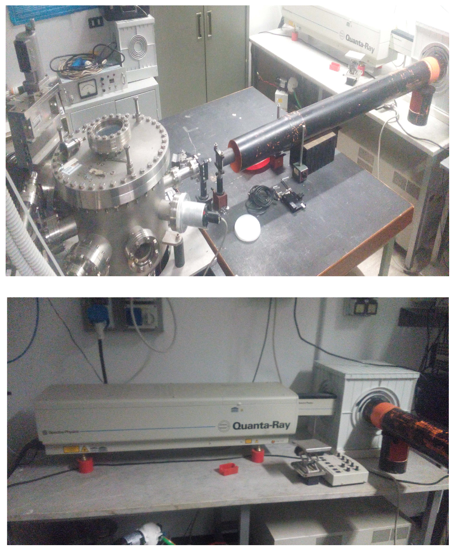
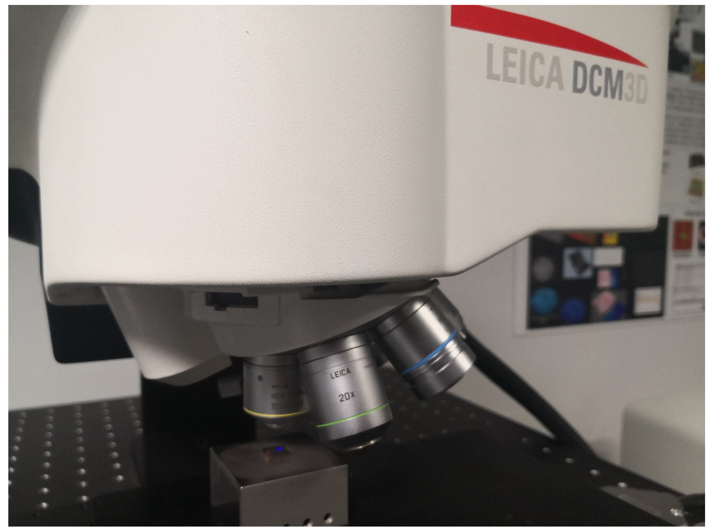
2. Materials and Methods

Molybdenum oxide (MoO3) thin films have been deposited by pulsed-laser deposition (PLD) starting from a commercial MoO3 target. In Figure 1 we show the laser system available at the Istituto Struttura della Materia of CNR, a Nd:Yag operating at 355 nm with a pulse duration of 7 ns, an energy density of 2 J/cm2, and a repetition rate of 10 Hz. The deposition chamber shown in Figure 1 is a cylindrical volume with a top flange used as a viewport and with six lateral flanges. It is equipped with both a multi-target system and a substrate heater allowing the deposition of the films up to 900 °C. During the deposition, the target can be rotated for getting more uniform films.
Six MoO3 films have been deposited onto smooth Cu substrates at different substrate temperatures (Ts), ranging from 300 to 400 °C, as measured by the temperature controller and monitored by an optical pyrometer. The target-to-substrate distance was set to 5 cm. The deposition chamber was evacuated to a base pressure of 10−7 mbar prior to film deposition and pure oxygen gas was introduced inside the chamber during the deposition. The oxygen partial pressure was in the range 0.01–0.2 mbar and the deposition time was also changed to study the effect of growth temperature on the structural and electrical characteristics of these films. The deposition parameters of the films deposed by PLD are listed in Table 1.

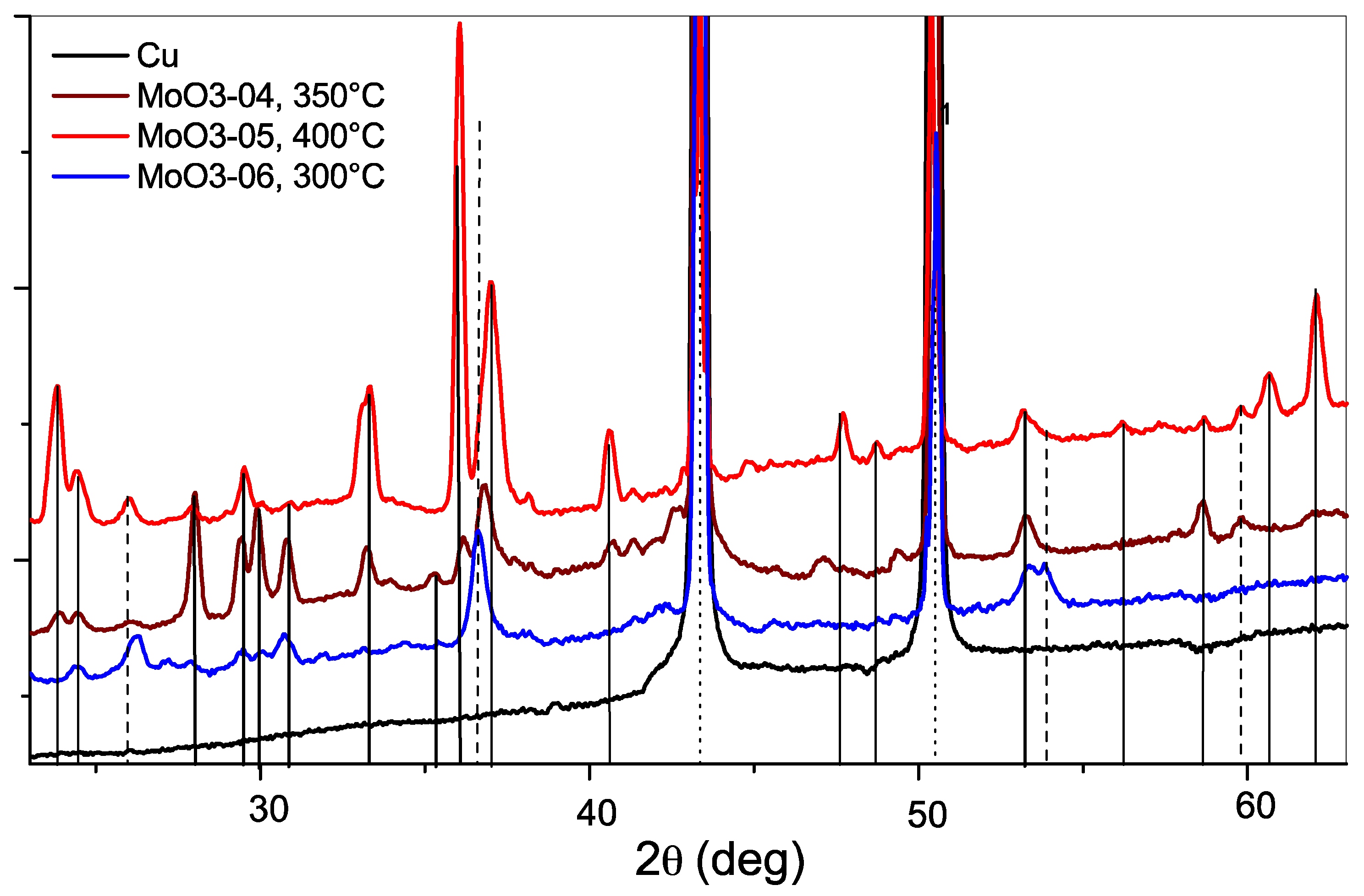
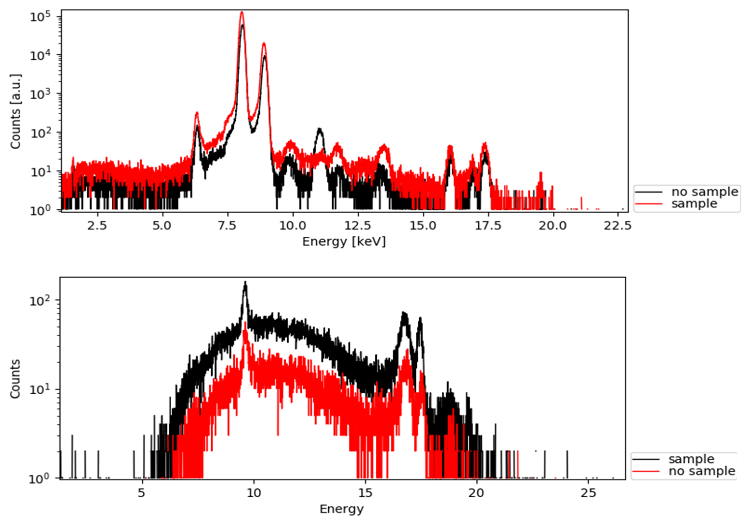
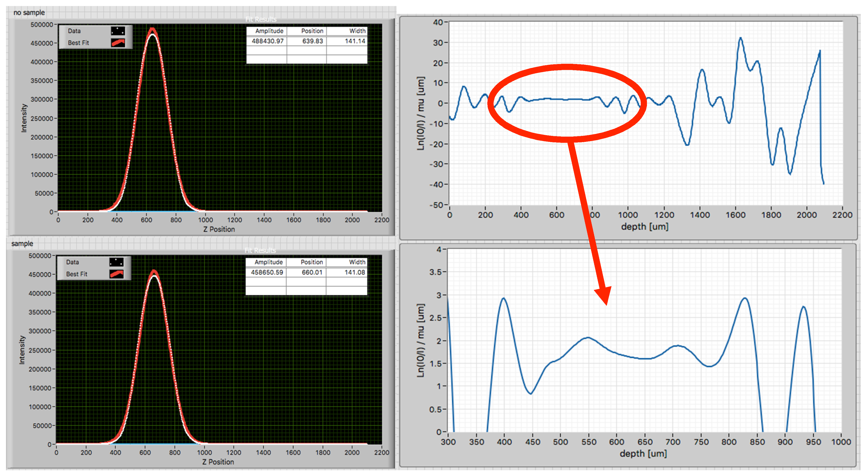
3. Results and Discussion

The XRD patterns of three films—MoO3-04, MoO3-05, and MoO3-06—are compared in Figure 2, collected with the θ–2θ scan mode. The films grown at lower oxygen pressures (10−3 mbar—not shown) mainly exhibit the peaks of the MoO2 phase, whereas at O2 pressures of ~0.1 mbar, the peaks characteristic of the MoO3 phase also appear. The effect of the deposition temperature Ts, at the O2 pressure of 0.1 mbar, is evident from the XRD spectra: At 300° C and 20 min of deposition (MoO3-06), we observe a coexistence of both phases, whereas at 350° C and 10 min of deposition (MoO3-04), the MoO3 phase prevails on the MoO2 one. At Ts = 400° C and 10 min of deposition (MoO3-05), the data of the film clearly shows the presence of the MoO3 phase with a high degree of order. Actually, these films are complex nanophase systems where molybdenum may exist in several oxidation states: Mo4+, Mo5+, and Mo6+, and whose valence and structure also change with the temperature and the annealing treatments. To enhance the order of the existing phases, different thermal treatments could be performed [25].

3.1. Evaluation of MoO3 Films Thicknesses

MoO3 coated on copper by physical vapor deposition in vacuum without thermal annealing mainly grows as a disordered film [25,26]. To characterize the quality of these films deposed by PLD [27,28,29], we also performed X-ray fluorescence (XRF) experiments at the XlabF RXR facility of LNF, based on a confocal set that was characterized by probing a spherical object of ~80 µm diameter [21]. The experimental parameters with the conventional molybdenum anode source were determined by the time acquisition per point 180 sec, the applied voltage V= 40 kV, and the current I = 950 µA. To measure the coatings and the copper substrate we chose two points, one on the copper surface and the other one on the coated copper, as shown in Figure 3.
Actually, with this layout it is not possible to perform a quantitative analysis of a sample. However, thanks to the ability of the RXR setup in a 3D analysis and thanks to the copper substrate, we performed the absorption fluorescence analysis by a depth scan.
In Figure 4 (top), the XRF spectra collected on copper and on the oxide coating were compared. Peaks with similar relative intensities appeared at 9.8, 11, 11.5, 13, and 16 keV, compared to the peak at 11 keV, which was stronger on the copper surface. This peak and the Cu peak relative areas were used to evaluate the MoO3 film thickness. In particular, we evaluated the peak area for each position vs. depth (i.e., along the Z axis), measuring the beam intensity with and without the coated film. Using the same method, we evaluated the MoO3 thickness of one film coated on sapphire. In Figure 4 (bottom), the XRF spectrum of the MoO3 film growth on the substrate of sapphire is compared with the XRF spectrum without the coating. Actually, since the copper substrate was replaced by the sapphire and due to the very low efficiency of the RXR confocal setup at low energy, we could not apply the same method to evaluate the thickness of the coating.
From the Cu fluorescence intensity ratio (i.e., from the I0/I ratio of the Moseley law [30], assuming to know the absorption coefficient of MoO3), we can estimate the sample thickness. In the left panel of Figure 5, the integrated Cu fluorescence intensities vs. depth are shown, while in the right panel, the path length obtained by the Moseley equation is shown. To evaluate the film thickness, in Figure 5 we considered only the region highlighted in red, where the confocal beam starts to probe the sample (i.e., > 400 µm). Data were stable and constant for ~400 µm, while after that the probe was totally absorbed by the copper substrate. The flat region in the top right panel corresponds to 1.71 ± 0.45 μm and can be interpreted as the real path that the fluorescence radiation travels from the copper substrate to reach the surface of the film. Since the radiation was not hitting the surface along the normal direction [31], from trigonometrical consideration we can obtain both the path travelled by the fluorescence radiation inside the film (l) and the thickness of the MoO3 film (x = 0.86 ± 0.30 μm).

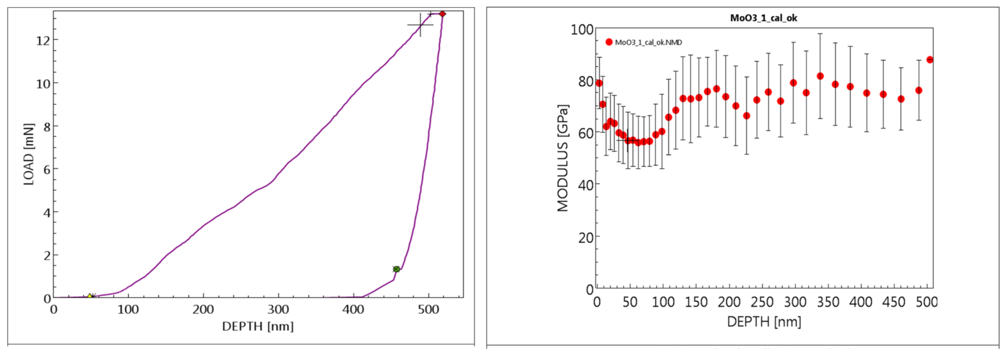
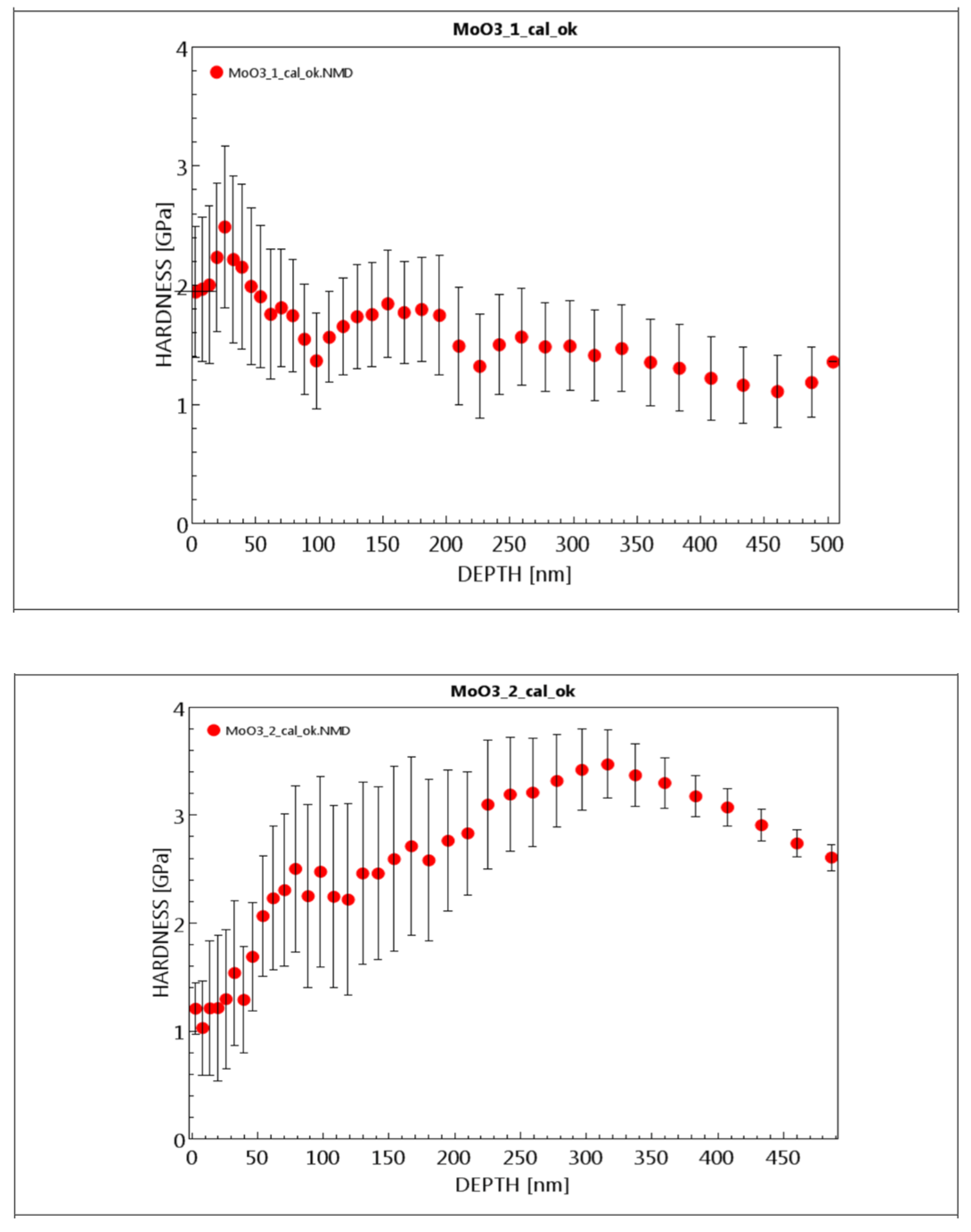
3.2. Study of Mechanical Properties of MoO3 Films on Copper

The study of the mechanical properties of these MoO3 films (see Figure 6) was performed at the LIME laboratory of the Roma Tre University using confocal optical profiling and nano-indentation methods. Nanoindentation tests were performed using a KLA-Tencor iNano NanoIndenter, equipped with an inForce 50 mN actuator and a Berkovich tip using the standard Continuous Stiffness Measurement (CSM) method and the Oliver and Pharr analytical model [32,33,34,35]. Nanoindenter frame stiffness and tip area function were calibrated by testing on a fused quartz reference sample, according to the ISO 14,577 standard. For the standard CSM tests, a grid of 15 indents was realized over a squared area of 30 × 50 μm2, with a spacing of 10 μm and a maximum indentation depth of 500 nm. The analysis was performed with the parameters listed in Table 2.
Surface morphology and surface roughness were measured by optical microscopy and confocal profilometer analyses. A Leica DCM 3D optical profilometer, equipped with a 50× optical objective, was used to calculate the surface roughness parameters of interest, analyzing four different zones on each sample (each single zone has an area of 250 × 200 µm2). Confocal profilometer analysis was realized starting from the Ra-measured values. This made it possible to select the indentation depth (to use as input in the nanoindentation test) and to reduce both the effects of surface roughness (more evident at shallower depths) and the ones due to porosity (more important at larger depths) on the modulus (or hardness) vs. depth profile.
As reported in Table 3, the analysis of the MoO3-01 and MoO3-02 films returns a higher roughness for the MoO3-01 sample with respect to MoO3-02 sample.
Concerning the hardness and the elastic modulus, we measured them as function of the depth for both samples. Figure 7 and Figure 8 show the plots of the load and of the modulus and of these two samples.
The hardness and elastic modulus values of these films can be extrapolated from the zero value of depth (x axis) in the plot or as the average of the three first measured values (Figure 7, Figure 8 and Figure 9). The choice of the first three measured points was made according to the thickness of the oxide (which was supposed to be very small), but it could be changed depending on the coating thickness. As a general rule, the indentation depth used for the modulus and hardness calculation is between 1 and 10% of the coating thickness, not more than 10%, otherwise substrate effects will be included. The results of the mechanical analysis depend on the copper substrate conditions. Indeed the two samples analyzed have, in principle, the same copper substrate, but they show a different hardness value related to the maximum depth. This result is likely due to the different parameters of the PLD process. The elastic modulus and the hardness as a function of depth highlight the dependence on the roughness, thickness, and homogeneity of these molybdenum oxide films and of the substrate. The two copper substrate are not “completely” alike: The material is the same, as obviously described in the modulus vs. depth curves, observing the same value for the same final depth (correct for copper) that refers mainly to the substrate. But for the hardness, things change: For 500 nm depth (where the substrate dominates the measured values), the hardness value is different. Hardness, which is an extensive property (not intensive as the modulus), could be affected by substrate surface finishing or mechanical/thermal treatments and this reflects in the measured hardness values, which are different for the two samples. This is clearer observing the error bars on the hardness vs. depth curves: They are small in sample 2, which is the one that exhibits smaller roughness (Ra value in Table 3). The roughness of the coating depends on the growth mechanisms, but it depends also on the substrate surface condition and finishing. In this case it seems that the two substrates are not completely similar, reflecting the mechanical properties on the coating (combined with the growth mechanism) due to the different surface roughness.

4. Conclusions

The great interest towards molybdenum trioxide is due to its mechanical resistance, good electrical conductivity for small thicknesses, and its low field emission thanks to its very high work function. The characterization of MoO3 thin films is important in spite of molybdenum trioxide (MoO3) being a hard transparent insulator. The very thin layer of MoO3 oxides grown on thick copper substrates became a conductive coating while still maintaining a high work function (~7 eV) [25]. Because of the high work function, copper devices with thin oxide films coated on their surface could be used in accelerating devices to reduce the dark current [26] (i.e., the emission of electrons from the surface). In this document we report an investigation of temperature vs. O2 pressure conditions of MoO3 films growth by PLD, starting from commercial MoO3 targets. We found that for nanophase oxide films with a thickness higher than 1 μm, as characterized by XRF spectra, the presence of a MoO3 phase with a high crystallinity degree is obtained when the substrate is heated at a temperature of 400 °C and with an O2 pressure of 0.1 mbar. In addition, the mechanical characterizations of hardness and elastic modulus of these films show a dependence on the probe type used. Efforts are needed to improve the homogeneity of the film thickness and, in particular, to improve the roughness, which is associated to the different behaviors of the different oxide phases, and which is particularly important to minimize the breakdown phenomena. Finally, in order to prevent possible contaminations and to obtain control of the oxidation, we underline that the vacuum in the deposition chamber has to be ~10−8 mbar or less. Further characterizations of MoO3 films with thickness > 1 μm on copper substrates are planned to check the stability, mechanical resistance, and chemical properties of these extremely interesting molybdenum oxide films. Furthermore, testing of RF structures with high gradient electric fields are proposed to verify the MoO3 films’ robustness and stability.

Author Contributions

Conceptualization and methodology, J.S., S.M., A.M., B.S. and L.F.; data analysis, D.H., S.D., S.S., A.D.T. and R.M.; manuscript preparation: J.S., S.M., A.M. and B.S.; all authors have reviewed the manuscript.

Funding

This research received no external funding.

Acknowledgments

We kindly acknowledge C. Veroli for his support with XRD measurements. A special thanks is due to E. Benporad of the ROMA TRE Electron Microscopy Laboratory (LIME).

Conflicts of Interest

The authors declare no conflicts of interest.

References

  1. Graedel, T.E.; Harper, E.M.; Nassar, N.T.; Reck, B.K. On the materials basis of modern society. Proc. Natl. Acad. Sci. USA 2013, 112, 6295–6300. [Google Scholar] [CrossRef] [PubMed]
  2. Pritzkau, D.P.; Siemann, R.H. Experimental study of rf pulsed heating on oxygen free electronic copper. Phys. Rev. Spec. Top. Accel. Beams 2002, 5, 112002. [Google Scholar] [CrossRef]
  3. Carter, R.G. Acceleration technologies for charged particles: An introduction. Contemp. Phys. 2011, 52, 15–41. [Google Scholar] [CrossRef]
  4. Döbert, S.; Adolphsen, C.; Bowden, G.; Burke, D.; Chan, J.; Dolgashev, V.; Frisch, J.; Jobe, K.; Jones, R.; Lewandowski, J.; et al. High Gradient Performance of NLC/GLC X-Band Accelerating Structures. In Proceedings of the 2005 Particle Accelerator Conference, Knoxville, TN, USA, 16–20 May 2005. [Google Scholar]
  5. Bini, S.; Chimenti, V.; Marcelli, A.; Palumbo, L.; Spataro, B.; Dolgashev, V.A.; Tantawi, S.; Yeremian, A.D.; Higashi, Y.; Grimaldi, M.G.; et al. Development of X-band accelerating structures for high gradients. Chin. Phys. C 2012, 36, 639–647. [Google Scholar] [CrossRef]
  6. Kwan, T.; Dawson, J.M.; Lin, A.T. Free electron laser. Phys. Fluids 1997, 36, 486–506. [Google Scholar]
  7. Deacon, D.A.G.; Elias, L.R.; Madey, J.M.J.; Ramian, G.J.; Schwettman, H.A.; Smith, T.I. First Operation of a Free-Electron Laser. Phys. Rev. Lett. 1977, 38, 892–894. [Google Scholar] [CrossRef]
  8. Antoine, C.Z.; Peauger, F.; Le Pimpec, F. Electromigration occurrences and its effects on metallic surfaces submitted to high electromagnetic field: A novel approach to breakdown in accelerators. Nucl. Instrum. Methods Phys. Res. Sect. A 2011, 665, 54–69. [Google Scholar] [CrossRef]
  9. Knobloch, J. Advanced Thermometry Studies of Superconducting Radio Frequency Cavities. Ph.D. Thesis, Cornell University, Ithaca, NY, USA, 1997; p. 285. [Google Scholar]
  10. Norem, J.; Insepov, Z.; Konkashbaev, I. Triggers for RF breakdown. Nucl. Instrum. Methods Phys. Res. Sect. A 2005, 537, 510–520. [Google Scholar] [CrossRef]
  11. Insepov, Z.; Norem, J.; Proslier, T.; Huang, D.; Mahalingam, S.; Veitzer, S. Modeling RF breakdown arcs. arXiv 2011, arXiv:1003.1736. [Google Scholar]
  12. Dolgashev, V.A.; Tantawi, S.G.; Nantista, C.D.; Higashi, Y.; Higo, T. RF breakdown in normal conducting single-cell structures. In Proceedings of the 2005 Particle Accelerator Conference, Knoxville, TN, USA, 16–20 May 2005. [Google Scholar]
  13. Wang, J.W. R&D of Accelerator Structures at SLAC; SLAC-PUB-12293; Stanford Linear Accelerator Center (SLAC): Menlo Park, CA, USA, 2007. [Google Scholar]
  14. Guignard, G. CLIC Study Team. CERN 2000-008. July 2000. [Google Scholar]
  15. Dolgashev, V.; Tantawi, S.; Yeremian, A.; Higashi, Y.; Spataro, B. Status of high power tests of normal conducting single-cell standing wave structures. In Proceedings of the 1st International Particle Accelerator Conference (IPAC 2010), Kyoto, Japan, 23–28 May 2010. [Google Scholar]
  16. Dolgashev, V.A. High Gradient, X-Band and above, Metallic RF structures. In Proceedings of the AAC2015, Isola d’Elba, Italy, 13–19 September 2015. [Google Scholar]
  17. Belli, E.; Pinto, P.C.; Rumolo, G.; Sapountzis, A.; Sinkovits, T.; Taborelli, M.; Spataro, B.; Zobov, M.; Castorina, G.; Migliorati, M. Electron cloud buildup and impedance effects on beam dynamics in the Future Circular e+e Collider and experimental characterization of thin TiZrV vacuum chamber coatings. Phys. Rev. Accel. Beams 2018, 21, 111002. [Google Scholar] [CrossRef]
  18. Ferrario, M.; Alesini, D.; Anania, M.; Artioli, M.; Bacci, A.; Bartocci, S.; Bedogni, R.; Bellaveglia, M.; Biagioni, A.; Bisesto, F.; et al. EuPRAXIA@SPARC_LAB Design study towards a compact FEL facility at LNF. Nuclear Instrum. Methods Phys. Res. Sect. A 2018, 909, 134–138. [Google Scholar] [CrossRef]
  19. Vaccarezza, C.; Alesini, D.; Bacci, A.; Cianchi, A.; Chiadroni, E.; Croia, M.; Diomede, M.; Ferrario, M.; Gallo, A.; Giribono, A.; et al. EUPRAXIA@SPARC_LAB: Beam dynamics studies for the X-band Linac. Nuclear Instrum. Methods Phys. Res. Sect. A 2018, 909, 314–317. [Google Scholar] [CrossRef]
  20. Giribono, A.; Bacci, A.; Chiadroni, E.; Cianchi, A.; Croia, M.; Ferrario, M.; Marocchino, A.; Petrillo, V.; Pompili, R.; Romeo, S.; et al. EuPRAXIA@SPARC_LAB: The high-brightness RF photo-injector layout proposal. Nuclear Instrum. Methods Phys. Res. Sect. A 2018, 909, 282–285. [Google Scholar] [CrossRef]
  21. Marcelli, A.; Spataro, B.; Sarti, S.; Dolgashev, V.A.; Tantawi, S.; Yeremian, D.A.; Higashi, Y.; Parodi, R.; Notargiacomo, A.; Xu, J.; et al. Characterization of thick conducting molybdenum films: Enhanced conductivity via thermal annealing. Surf. Coat. Technol. 2015, 261, 391–397. [Google Scholar] [CrossRef]
  22. Cahill, A.; Dolgashev, V.; Rosenzweig, J.; Tantawi, S.; Weathersby, S. Ultra high gradient breakdown rates in X-Band cryogenic normal conducting RF accelerating cavities. In Proceedings of the 8th International Particle Accelerator Conference (IPAC 2017), Copenhagen, Denmark, 14–19 May 2017; p. THPIK125. [Google Scholar]
  23. Marcelli, A.; Spataro, B.; Castorina, G.; Xu, W.; Sarti, S.; Monforte, F.; Cibin, G. Materials and Breakdown Phenomena: Heterogeneous Molybdenum Metallic Films. Condensed Matter 2017, 2, 18. [Google Scholar] [CrossRef]
  24. Orlandi, G.; Scalambrin, F.; Hauer, M.; Calatroni, S.; Benvenuti, C. Niobium coatings for 1.5 GHz RF cavities. No. CERN-MT-93-13-SM. P00019445. 1993. [Google Scholar]
  25. Macis, S.; Aramo, C.; Bonavolontà, C.; Cibin, G.; D’Elia, A.; Davoli, I.; De Lucia, M.; Lucci, M.; Lupi, S.; Miliucci, M.; et al. MoO3 films grown on polycristalline Cu: Morphological, structural, and electronic properties. J. Vac. Sci. Technol. A 2019, 37, 021513. [Google Scholar] [CrossRef]
  26. Macis, S. Deposition and Characterization of Thin MoO3 Films on Cu for Technological Applications. Ph.D. Thesis, Tor Vergata University, Rome, Italy, 2018. [Google Scholar]
  27. Sunu, S.; Prabhu, E.; Jayaraman, V.; Gnanasekar, K.; Gnanasekaran, T. Gas sensing properties of PLD made MoO3 films. Sens. Actuators B Chem. 2003, 94, 189–196. [Google Scholar] [CrossRef]
  28. Ramana, C.V.; Atuchin, V.V.; Pokrovsky, L.D.; Becker, U.; Julien, C.M. Structure and chemical properties of molybdenum oxide thin films. J. Vac. Sci. Technol. A 2007, 25, 1166–1171. [Google Scholar] [CrossRef]
  29. Ramana, C.V.; Julien, C.M. Chemical and electrochemical properties of molybdenum oxide thin films prepared by reactive pulsed-laser assisted deposition. Chem. Phys. Lett. 2006, 428, 114–118. [Google Scholar] [CrossRef]
  30. Hampai, D.; Cherepennikov, Y.M.; Liedl, A.; Cappuccio, G.; Capitolo, E.; Iannarelli, M.; Azzutti, C.; Gladkikh, Y.P.; Marcelli, A.; Dabagov, S.B. Polycapillary based µXRF station for 3D colour tomography. J. Instrum. 2018, 13, C04024. [Google Scholar] [CrossRef]
  31. Moseley, H.G.J.; Jeffreys, H.G. XCIII. The high-frequency spectra of the elements. Lond. Edinb. Dublin Philos. Mag. J. Sci. 1913, 26, 1024–1034. [Google Scholar] [CrossRef]
  32. Oliver, W.; Pharr, G. An improved technique for determining hardness and elastic modulus using load and displacement sensing indentation experiments. J. Mater. Res. 1992, 7, 1564–1583. [Google Scholar] [CrossRef]
  33. Doerner, M.F.; William, D.N. A method for interpreting the data from depth-sensing indentation instruments. J. Mater. Res. 1986, 1, 601–609. [Google Scholar] [CrossRef]
  34. Oliver, W.C.; Georges, M.P. Measurement of hardness and elastic modulus by instrumented indentation: Advances in understanding and refinements to methodology. J. Mater. Res. 2004, 19, 3–20. [Google Scholar] [CrossRef]
  35. Li, X.; Bharat, B. A review of nanoindentation continuous stiffness measurement technique and its applications. Mater. Charact. 2002, 48, 11–36. [Google Scholar] [CrossRef]
Figure 1. The pulsed-laser apparatus used for the depositions: The vacuum chamber (top) and the Nd:Yag laser (bottom).
Instruments 03 00061 g001
Figure 2. XRD spectra of MoO3 films deposited at different temperatures and deposition times (pO2 = 0.1–0.2 mbar). Continuous lines highlight the MoO3 phase peaks, whereas dash and dot lines identify the MoΟ3 (or mixed MoO3 + MoO2) phase and the Cu substrate peaks, respectively.
Instruments 03 00061 g002
Figure 3. The red spots in the two panels show the locations of the XRD measurement on the PLD coatings: Copper (left) and MoO3 (right) (color on line).
Instruments 03 00061 g003
Figure 4. Comparison of the XRF spectra of the MoO3 (red) and of the copper (black) (top). Comparison of the XRF spectra of MoO3 (red) and sapphire (black) (bottom).
Instruments 03 00061 g004
Figure 5. (Left) Integrated Cu fluorescence data vs. depth: Cu (top) and Cu/MoO3 (below) as showed in Figure 3 and Figure 4; (right) plots show the path length obtained by the Moseley equation.
Instruments 03 00061 g005
Figure 6. The sample during the profilometer analysis (Mo03-01 (sample #1) and Mo03-02 (sample #2) films on copper).
Instruments 03 00061 g006
Figure 7. MoO3-01—(left) the load and (right) the modulus as a function of depth.
Instruments 03 00061 g007
Figure 8. MoO3-02—(left) the load and (right) the modulus as a function of depth.
Instruments 03 00061 g008
Figure 9. The hardness vs. depth for MoO3-01 (top) and MoO3-02 (bottom) films.
Instruments 03 00061 g009
Table 1. List of the six samples of MoO3 deposed by pulsed-laser deposition (PLD).
FilmTs (°C)p(O2) (mbar)Deposition Time (min)
MoO3-0138010−315
MoO3-023702 × 10−322
MoO3-0336510−120
MoO3-0435010−110
MoO3-054002 × 10−120
MoO3-063002 × 10−120
Table 2. The input parameters of the nanoindentation analysis.
TipBerkovich
ModeStandard CSM
Indentation5 × 3 matrix
Max. depth500 nm
Table 3. The roughness parameters of the MoO3-01 and MoO3-02 films.
SampleSa (µm)Ra (µm)
MoO3-010.2010.175 ± 0.035
MoO3-020.1150.083 ± 0.019

