Quenching Circuit and SPAD Integrated in CMOS 65 nm with 7.8 ps FWHM Single Photon Timing Resolution

 , , ,
, , ,  and
and
Abstract
1. Introduction
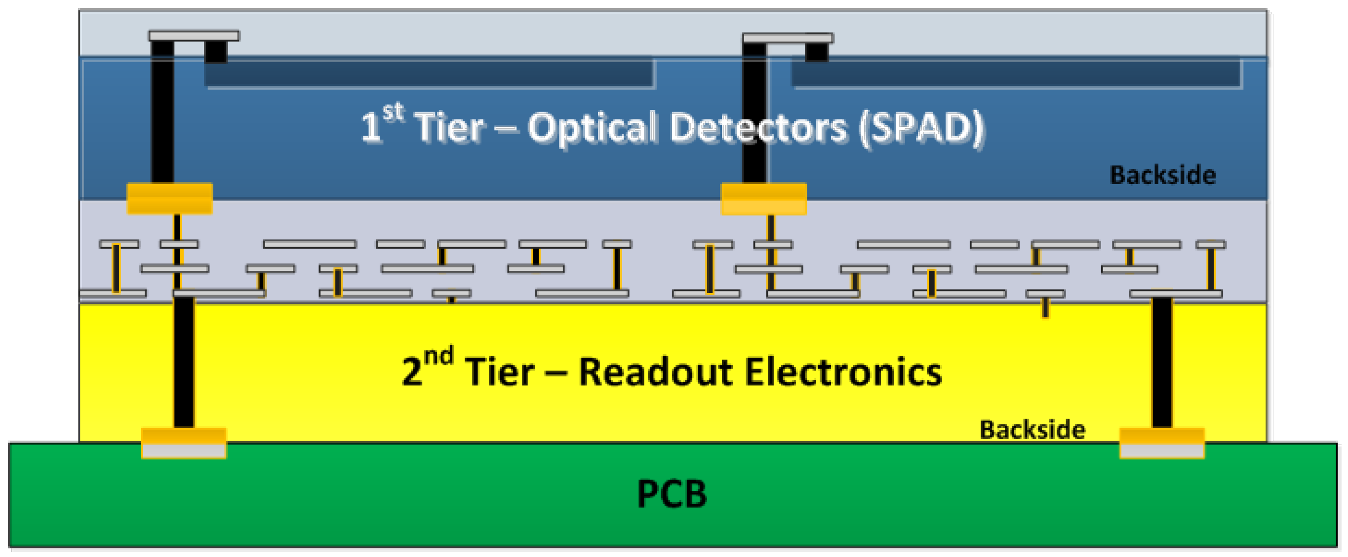
2. Architecture
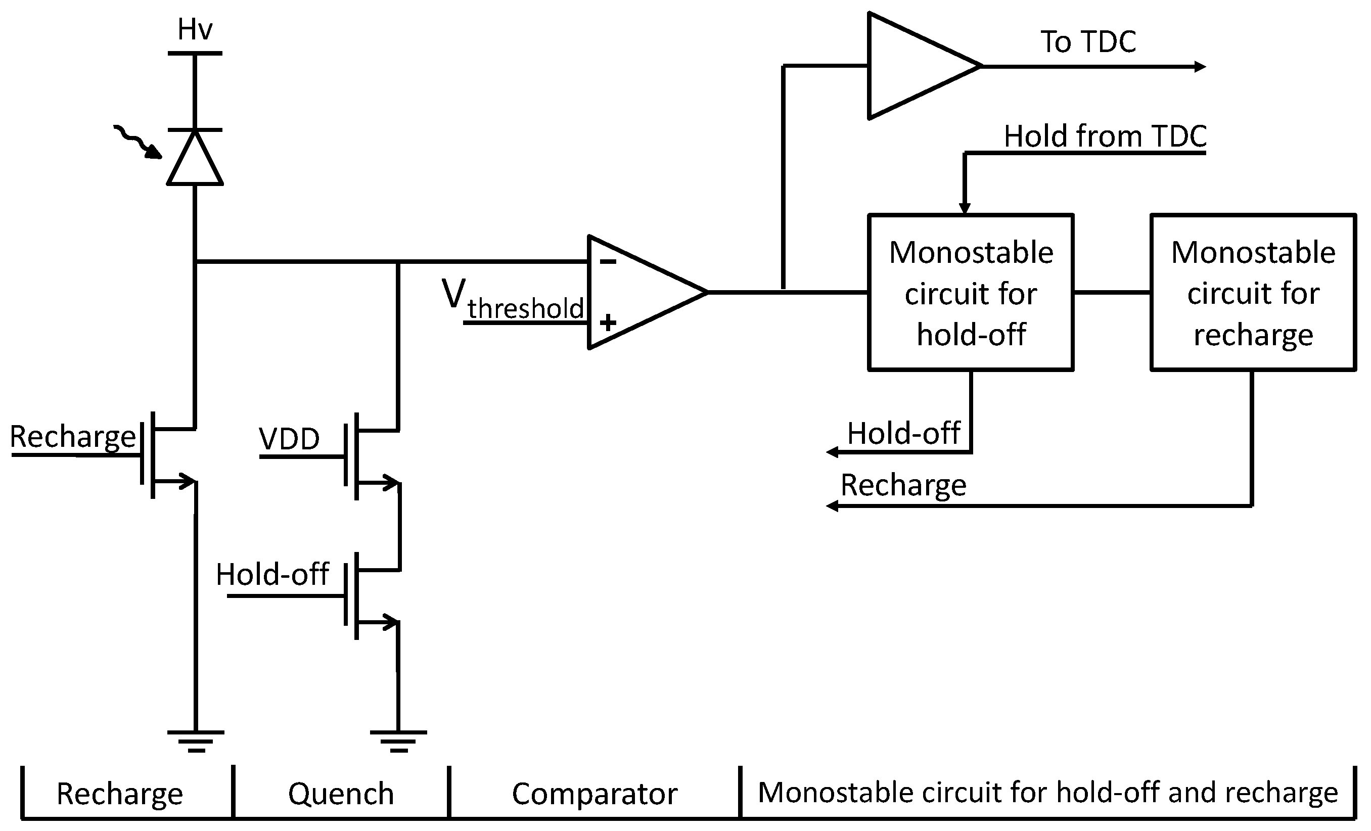
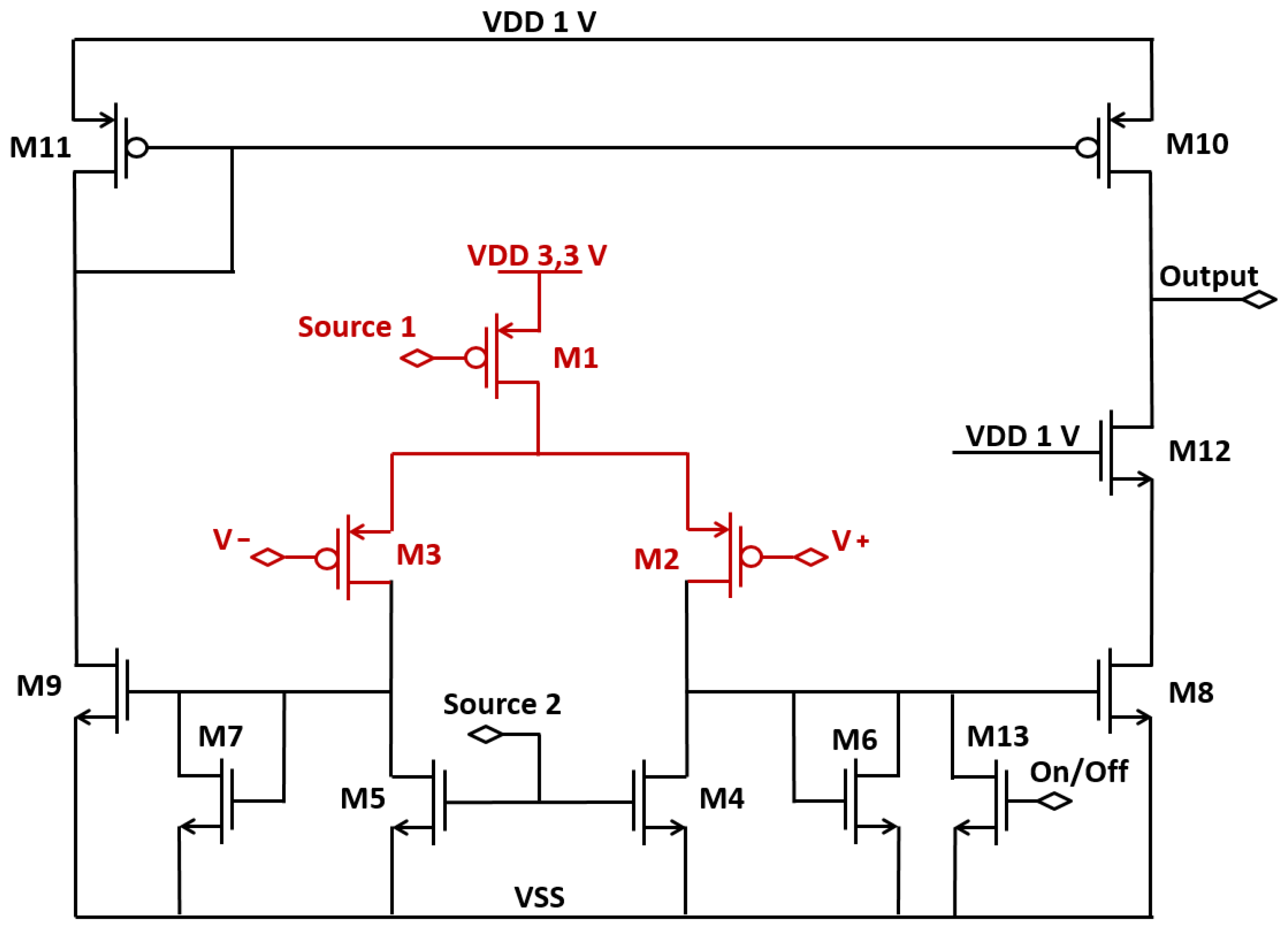
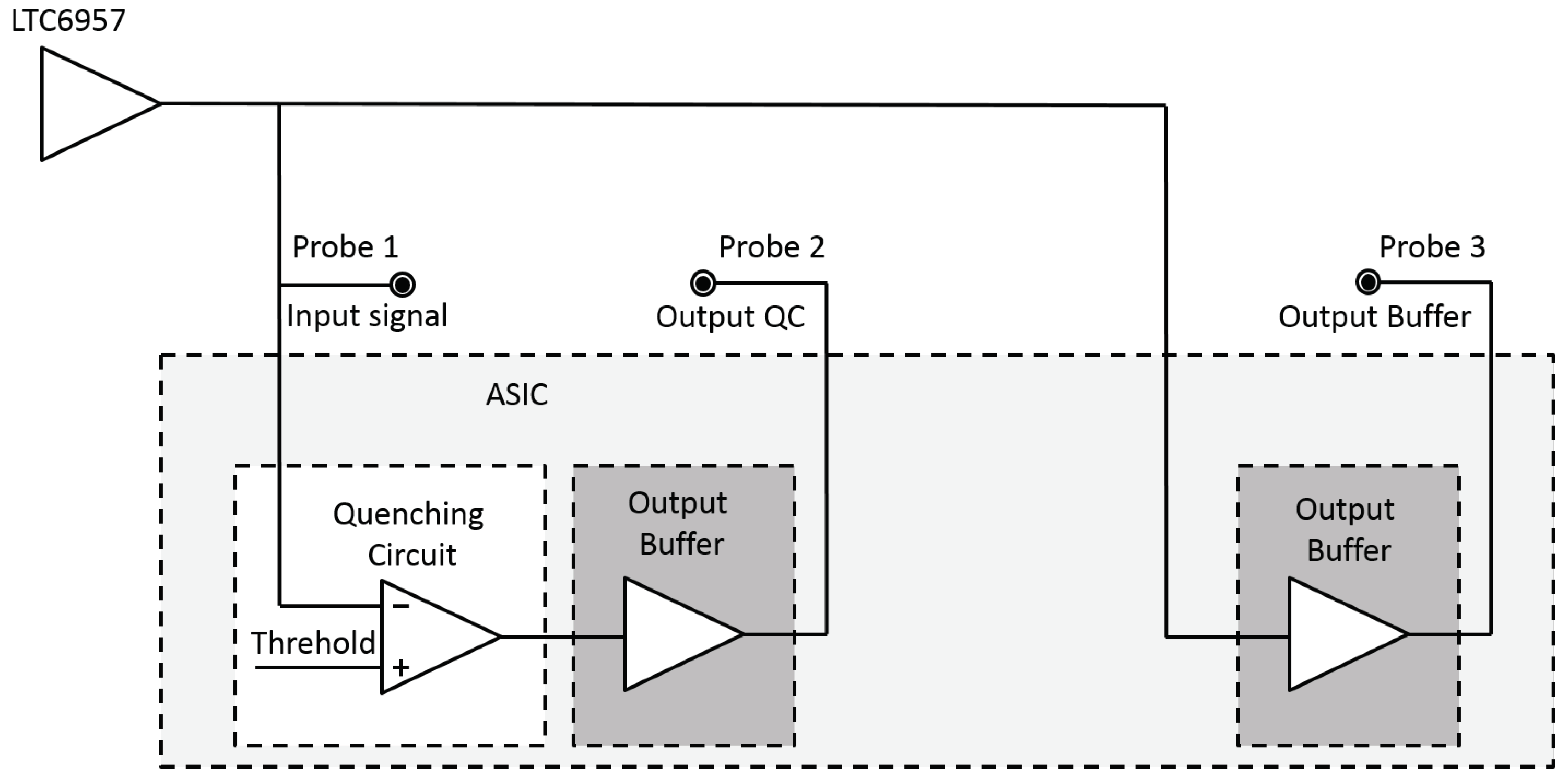
2.1. Quenching Circuit
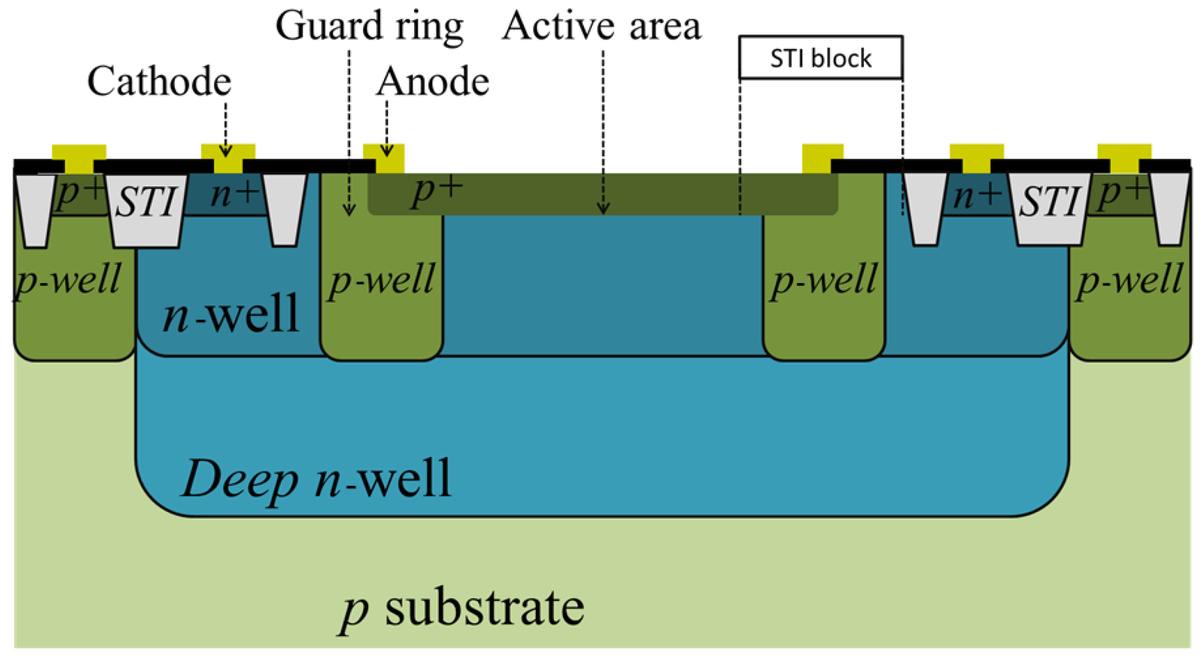
2.2. Single Photon Avalanche Diode
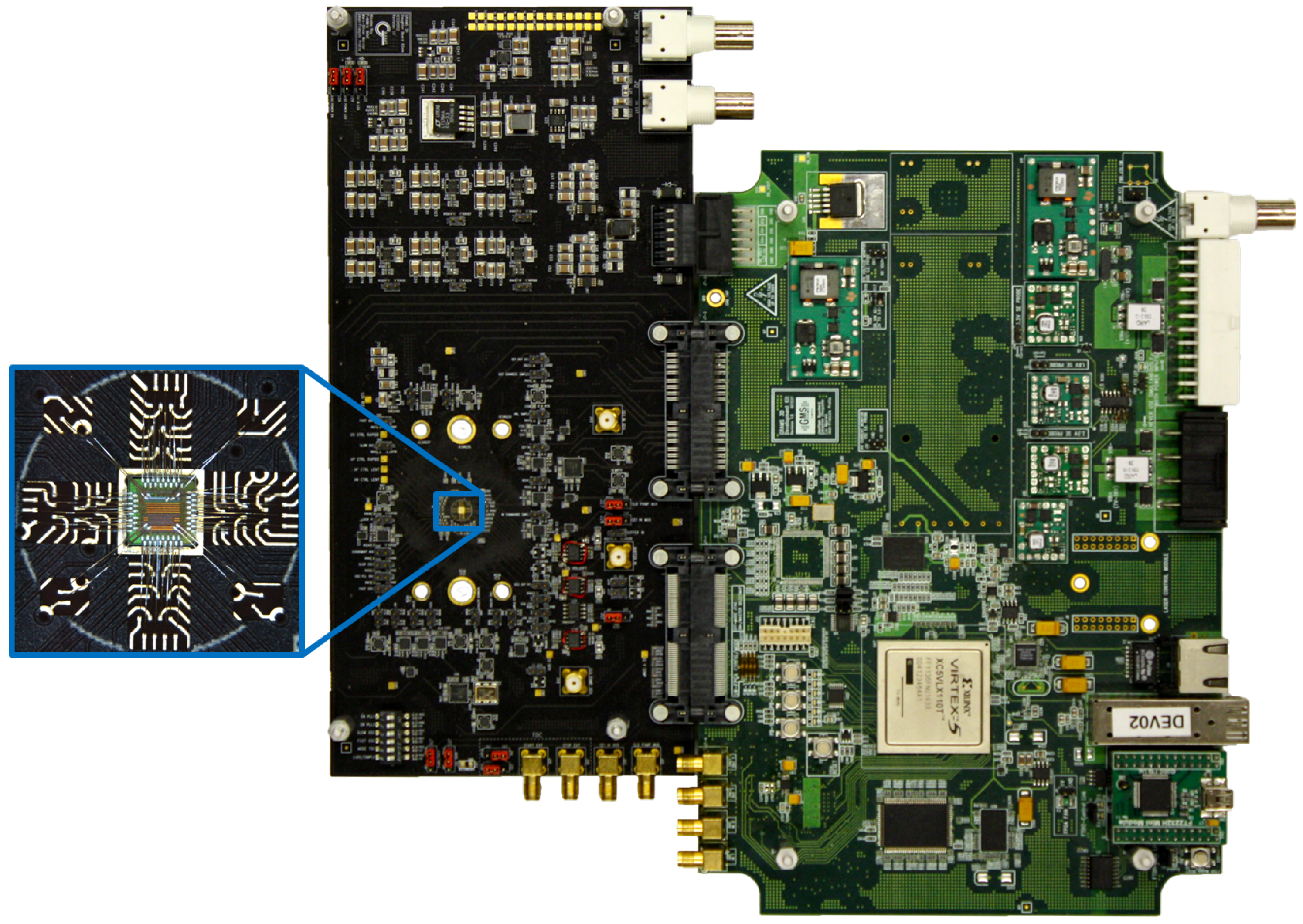
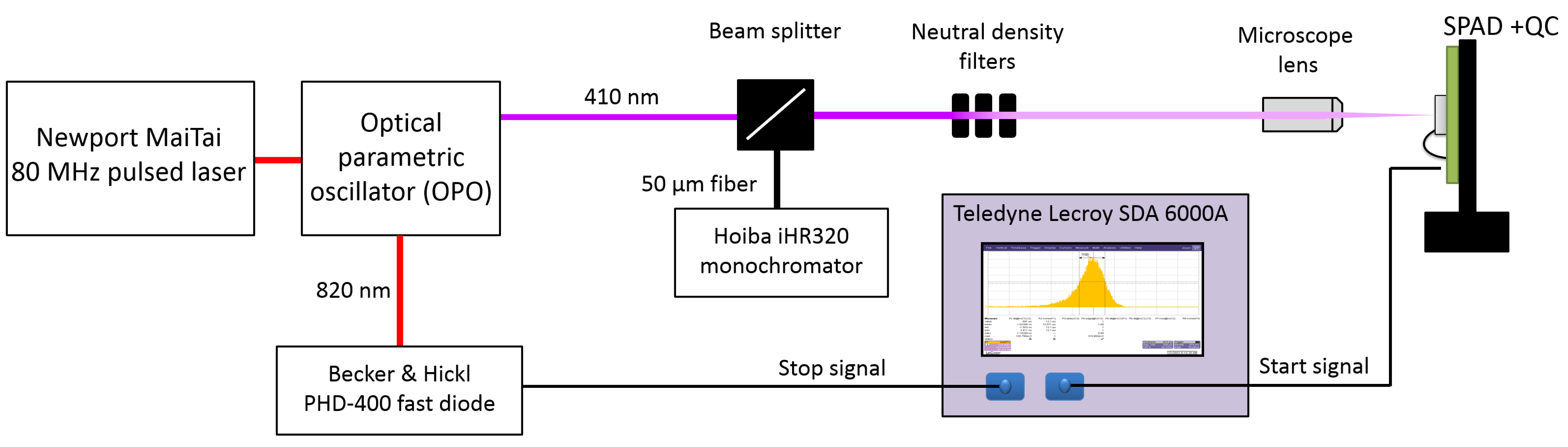
3. Materials and Methods
3.1. Quenching Circuit Characteristics
3.2. Quenching Circuit Electronic Timing Jitter
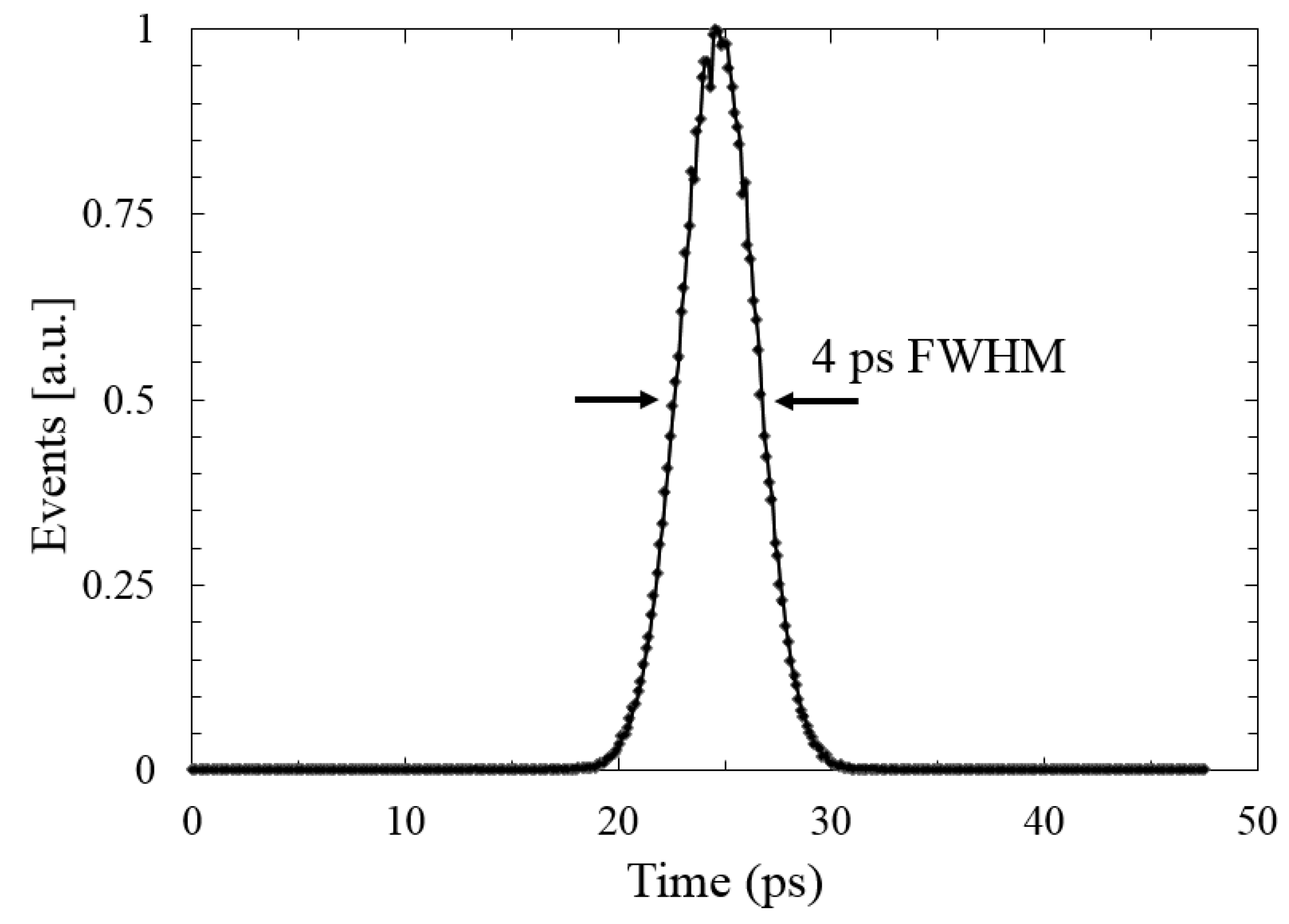
3.3. Single Photon Timing Resolution
3.4. SPAD Characteristics
3.5. SPAD Excess Voltage Variation
3.6. Timing Jitter Due to the SPAD Excess Voltage Variation
4. Results
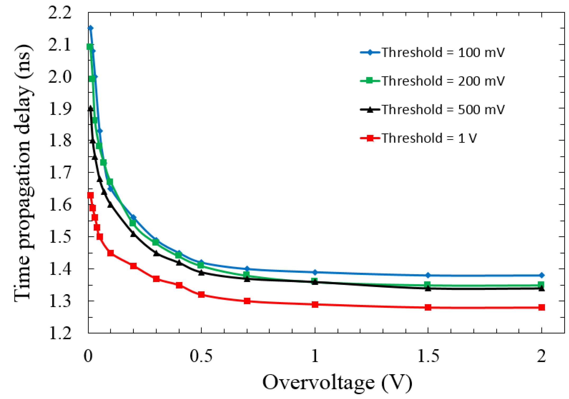
4.1. Quenching Circuit Characteristics
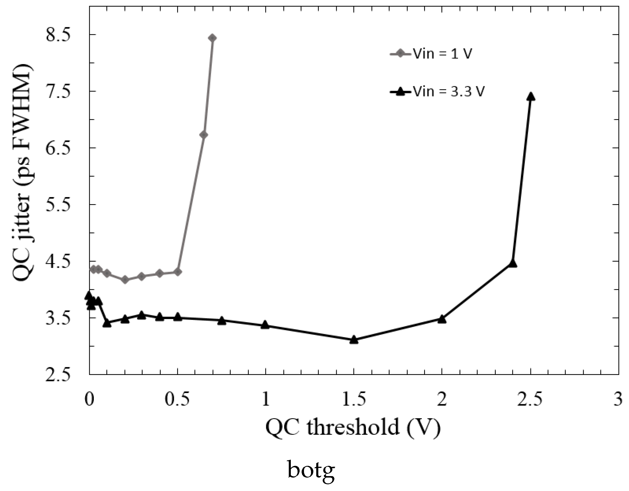
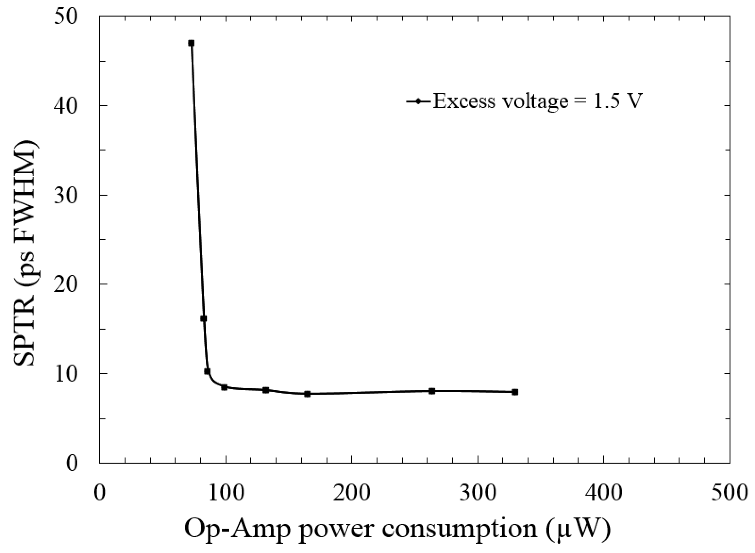
4.2. Quenching Circuit Electronic Timing Jitter
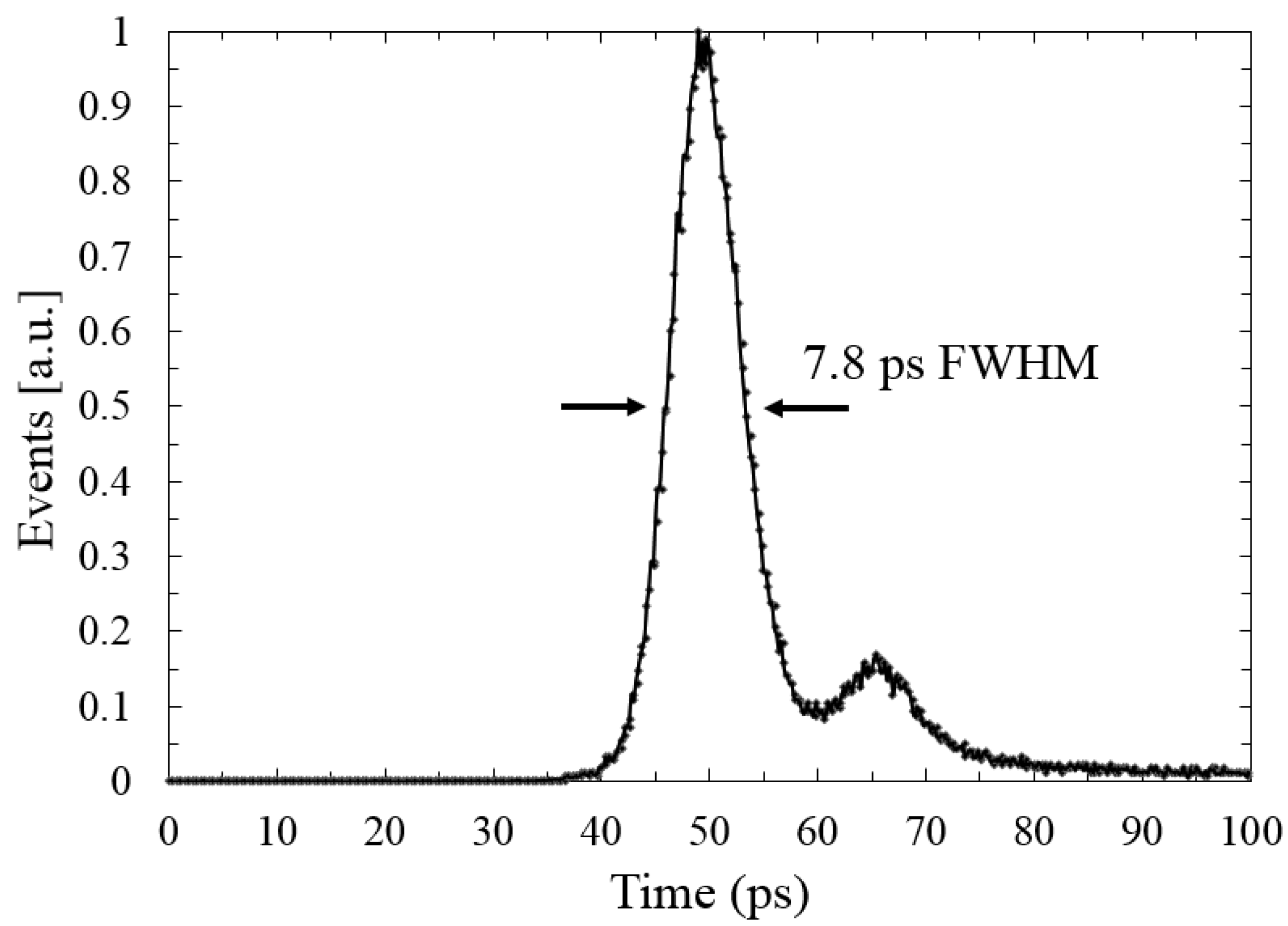
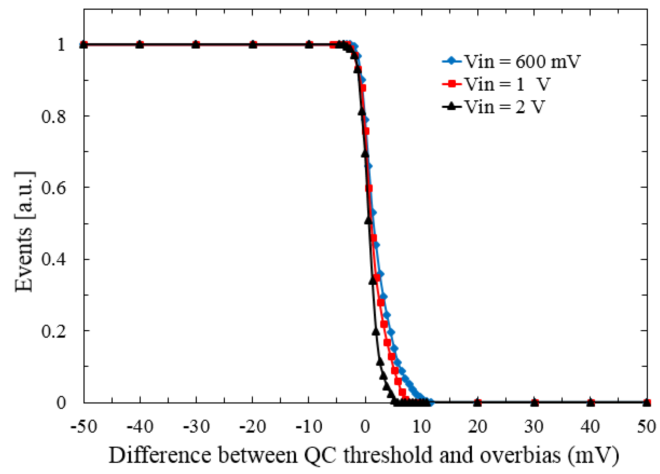
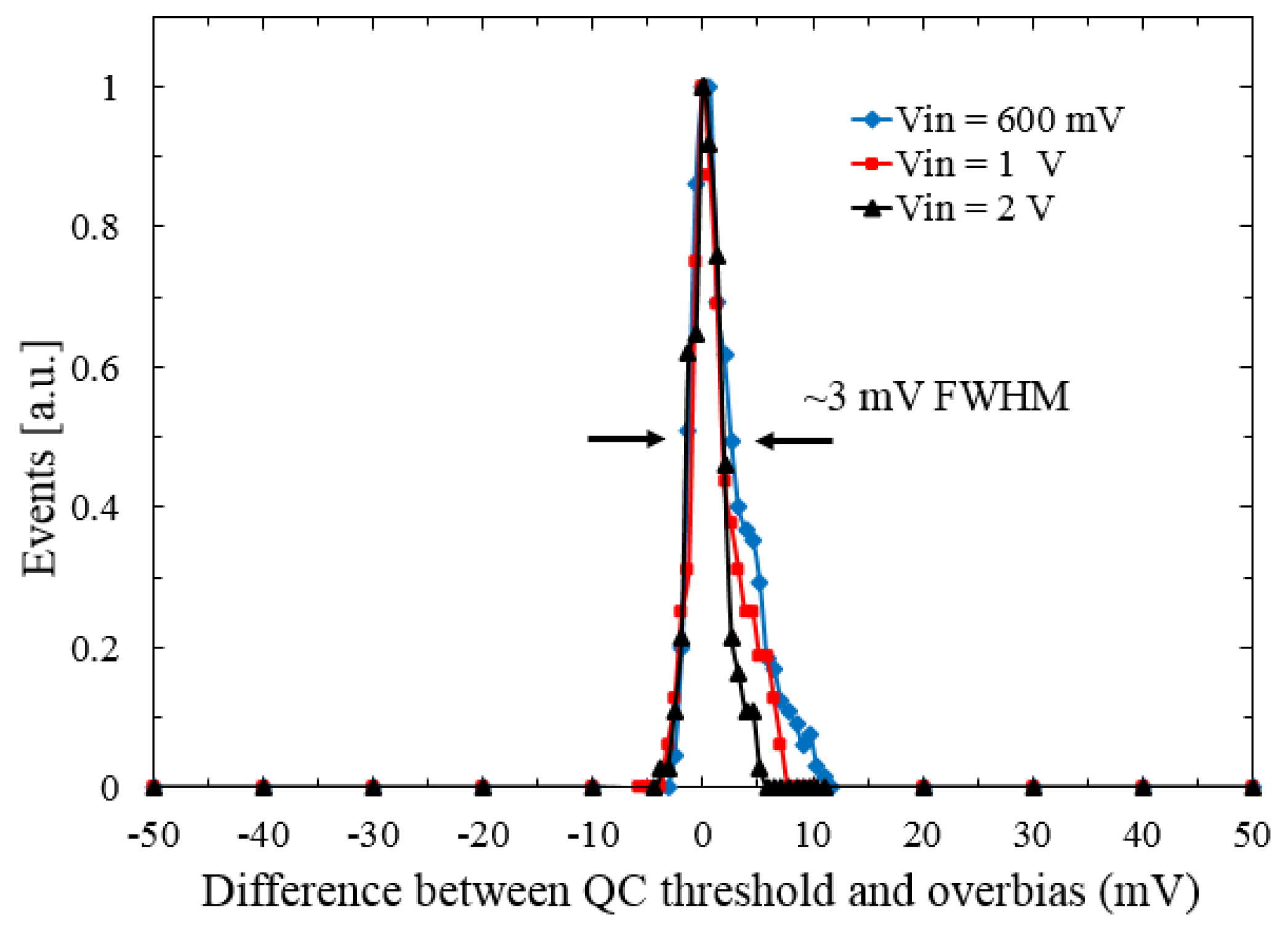
4.3. Single Photon Timing Resolution
4.4. SPAD Characteristics
4.5. SPAD Excess Voltage Variation
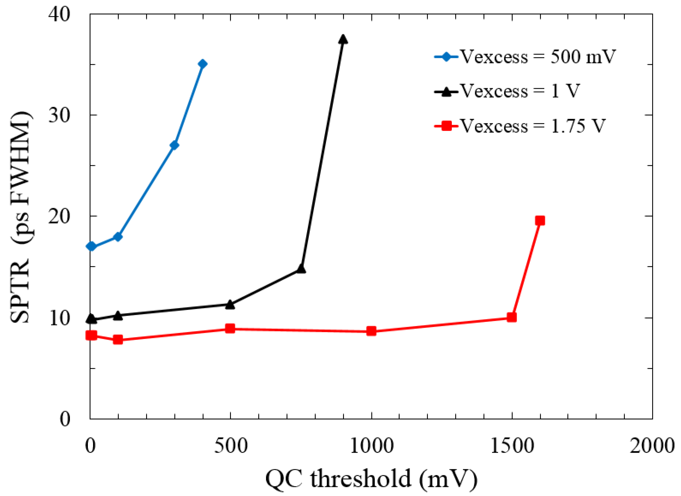
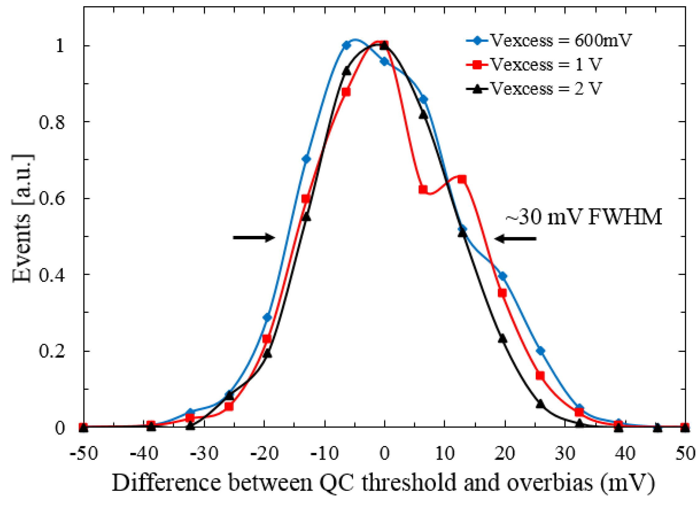
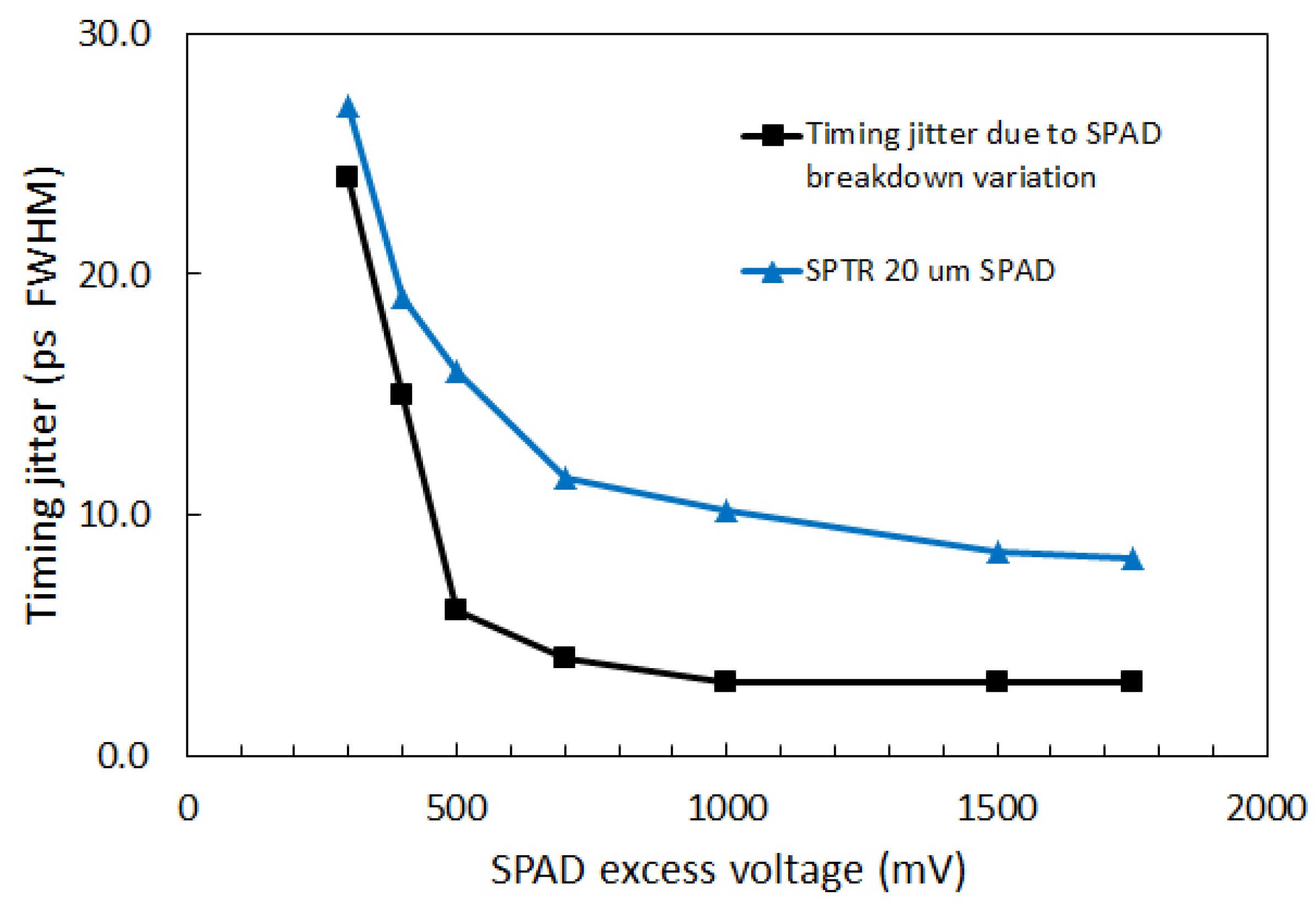
4.6. Timing Jitter Due to the SPAD Excess Voltage Variation
5. Discussion
6. Conclusions
Author Contributions
Acknowledgments
Conflicts of Interest
References
- Frach, T.; Prescher, G.; Degenhardt, C.; de Gruyter, R.; Schmitz, A.; Ballizany, R. The digital silicon photomultiplier—Principle of operation and intrinsic detector performance. In Proceedings of the Nuclear Science Symposium and Medical Imaging Conference (NSS/MIC), Orlando, FL, USA, 24 October–1 November 2009; pp. 1959–1965. [Google Scholar] [CrossRef]
- Schaart, D.R.; Charbon, E.; Frach, T.; Schulz, V. Advances in digital SiPMs and their application in biomedical imaging. Nucl. Instrum. Methods Phys. Res. Sec. A Accel. Spectrom. Detect. Assoc. Equip. 2016, 809, 31–52. [Google Scholar] [CrossRef]
- Bruschini, C.; Charbon, E.; Veerappan, C.; Braga, L.; Massari, N.; Perenzoni, M.; Gasparini, L.; Stoppa, D.; Walker, R.; Erdogan, A.; et al. SPADnet: Embedded coincidence in a smart sensor network for PET applications. Nucl. Instrum. Methods Phys. Res. Sec. A Accel. Spectrom. Detect. Assoc. Equip. 2014, 734, 122–126. [Google Scholar] [CrossRef]
- Powolny, F.; Auffray, E.; Brunner, S.E.; Garutti, E.; Goettlich, M.; Hillemanns, H.; Jarron, P.; Lecoq, P.; Meyer, T.; Schultz-Coulon, H.C.; et al. Time-based readout of a silicon photomultiplier (SiPM) for time of flight positron emission tomography (TOF-PET). IEEE Trans. Nucl. Sci. 2011, 58, 597–604. [Google Scholar] [CrossRef]
- Ronzhin, A.; Albrow, M.; Los, S.; Martens, M.; Murat, P.; Ramberg, E.; Kim, H.; Chen, C.T.; Kao, C.M.; Niessen, K.; et al. A SiPM-based TOF-PET detector with high speed digital DRS4 readout. Nucl. Instrum. Methods Phys. Res. Sec. A Accel. Spectrom. Detect. Assoc. Equip. 2013, 703, 109–113. [Google Scholar] [CrossRef]
- Gersbach, M.; Maruyama, Y.; Trimananda, R.; Fishburn, M.W.; Stoppa, D.; Richardson, J.A.; Walker, R.; Henderson, R.; Charbon, E. A time-resolved, low-noise single-photon image sensor fabricated in deep-submicron CMOS technology. IEEE J. Solid-State Circuits 2012, 47, 1394–1407. [Google Scholar] [CrossRef]
- Schwartz, D.E.; Charbon, E.; Shepard, K.L. A single-photon avalanche diode array for fluorescence lifetime imaging microscopy. IEEE J. Solid-State Circuits 2008, 43, 2546–2557. [Google Scholar] [CrossRef] [PubMed]
- Maruyama, Y.; Blacksberg, J.; Charbon, E. A 1024 × 8, 700-ps time-gated spad line sensor for planetary surface exploration with laser raman spectroscopy and libs. IEEE J. Solid-State Circuits 2014, 49, 179–189. [Google Scholar] [CrossRef]
- Nissinen, I.; Nissinen, J.; Keranen, P.; Lansman, A.K.; Holma, J.; Kostamovaara, J. A 2 × (4) × 128 Multitime-Gated SPAD Line Detector for Pulsed Raman Spectroscopy. IEEE Sens. J. 2015, 15, 1358–1365. [Google Scholar] [CrossRef]
- Fisher, E.; Underwood, I.; Henderson, R. A reconfigurable single-photon-counting integrating receiver for optical communications. IEEE J. Solid-State Circuits 2013, 48, 1638–1650. [Google Scholar] [CrossRef]
- Chitnis, D.; Collins, S. A SPAD-based photon detecting system for optical communications. J. Lightwave Technol. 2014, 32, 2028–2034. [Google Scholar] [CrossRef]
- Niclass, C.; Soga, M.; Kato, S. A 0.18 µm CMOS single-photon sensor for coaxial laser rangefinders. In Proceedings of the 2010 IEEE Asian Solid-State Circuits Conference, Beijing, China, 8–10 November 2010; pp. 105–108. [Google Scholar] [CrossRef]
- Bronzi, D.; Villa, F.; Tisa, S.; Tosi, A.; Zappa, F.; Durini, D.; Weyers, S.; Brockherde, W. 100,000 Frames/s 64 × 32 Single-Photon Detector Array for 2-D Imaging and 3-D Ranging. IEEE J. Sel. Top. Quantum Electron. 2014, 20, 354–363. [Google Scholar] [CrossRef]
- Stoppa, D.; Pancheri, L.; Scandiuzzo, M.; Gonzo, L.; Betta, G.F.D.; Simoni, A. A CMOS 3-D Imager Based on Single Photon Avalanche Diode. IEEE Trans. Circuits Syst. I Regul. Pap. 2007, 54, 4–12. [Google Scholar] [CrossRef]
- Moses, W.W. Time of flight in PET revisited. IEEE Trans. Nucl. Sci. 2003, 50, 1325–1330. [Google Scholar] [CrossRef]
- Gundacker, S.; Auffray, E.; Pauwels, K.; Lecoq, P. Measurement of intrinsic rise times for various L(Y)SO and LuAG scintillators with a general study of prompt photons to achieve 10 ps in TOF-PET. Phys. Med. Biol. 2016, 61, 2802. [Google Scholar] [CrossRef] [PubMed]
- Lecoq, P.; Korzhik, M.; Vasiliev, A. Can Transient Phenomena Help Improving Time Resolution in Scintillators. IEEE Trans. Nucl. Sci. 2014, 61, 229–234. [Google Scholar] [CrossRef]
- Omelkov, S.; Nagirnyi, V.; Vasilev, A.; Kirm, M. New features of hot intraband luminescence for fast timing. J. Lumin. 2016, 176, 309–317. [Google Scholar] [CrossRef]
- Grim, J.Q.; Christodoulou, S.; Di Stasio, F.; Krahne, R.; Cingolani, R.; Manna, L.; Moreels, I. Continuous-wave biexciton lasing at room temperature using solution-processed quantum wells. Nat. Nanotechnol. 2014, 9, 891–895. [Google Scholar] [CrossRef] [PubMed]
- Lecoq, P. Pushing the Limits in Time-of-Flight PET Imaging. IEEE Trans. Radiat. Plasma Med. Sci. 2017, 1, 473–485. [Google Scholar] [CrossRef]
- Ahmed, G.; Buhler, P.; Cargnelli, M.; Hohler, R.; Marton, J.; Orth, H.; Suzuki, K. Application of Geiger-mode photosensors in Cherenkov detectors. Nucl. Instrum. Methods Phys. Res. Sec. A Accel. Spectrom. Detect. Assoc. Equip. 2011, 639, 107–110. [Google Scholar] [CrossRef]
- Dolenec, R.; Korpar, S.; Krizan, P.; Pestonik, R.; Verdel, N. The Performance of Silicon Silicon Photomultipliers Photomultipliers in in Cherenkov. IEEE Trans. Nucl. Sci. 2016, 63, 2478–2481. [Google Scholar] [CrossRef]
- Frach, T. Optimization of the digital Silicon Photomultiplier for Cherenkov light detection. J. Instrum. 2012, 1, C01112. [Google Scholar] [CrossRef]
- Acerbi, F.; Ferri, A.; Gola, A.; Cazzanelli, M.; Pavesi, L.; Zorzi, N.; Piemonte, C. Characterization of Single-Photon Time Resolution: From Single SPAD to Silicon Photomultiplier. IEEE Trans. Nucl. Sci. 2014, 61, 2678–2686. [Google Scholar] [CrossRef]
- Nemallapudi, M.; Gundacker, S.; Lecoq, P.; Auffray, E. Single photon time resolution of state of the art SiPMs. J. Instrum. 2016, 11, P10016. [Google Scholar] [CrossRef]
- Acerbi, F.; Ferri, A.; Gola, A.; Zorzi, N.; Piemonte, C. Analysis of single-photon time resolution of FBK silicon photomultipliers. Nucl. Instrum. Methods Phys. Res. Sec. A Accel. Spectrom. Detect. Assoc. Equip. 2015, 787, 34–37. [Google Scholar] [CrossRef]
- Mandai, S.; Charbon, E. Optimization of the digital Silicon Photomultiplier for Cherenkov light detection. J. Instrum. 2013, 8, P09016. [Google Scholar] [CrossRef]
- Liu, Z.; Gundacker, S.; Pizzichemi, M.; Ghezzi, A.; Auffray, E.; Lecoq, P.; Paganoni, M. In-depth study of single photon time resolution for the Philips digital silicon photomultiplier. J. Instrum. 2016, 11, P06006. [Google Scholar] [CrossRef]
- Puill, V.; Bazin, C.; Breton, D.; Burmistrov, L.; Chaumat, V.; Dinu, N.; Maalmi, J.; Vagnucci, J.; Stocchi, A. Single photoelectron timing resolution of SiPM as a function of the bias voltage, the wavelength and the temperature. Nucl. Instrum. Methods Phys. Res. Sec. A Accel. Spectrom. Detect. Assoc. Equip. 2012, 695, 354–358. [Google Scholar] [CrossRef]
- Bérubé, B.L.; Rhéaume, V.P.; Therrien, A.C.; Parent, S.; Maurais, L.; Boisvert, A.; Carini, G.; Charlebois, S.A.; Fontaine, R.; Pratte, J.F. Development of a single photon avalanche diode (SPAD) array in high voltage CMOS 0.8 µm dedicated to a 3D integrated circuit (3DIC). In Proceedings of the 2012 IEEE Nuclear Science Symposium and Medical Imaging Conference Record (NSS/MIC), Anaheim, CA, USA, 27 October–3 November 2012; pp. 1835–1839. [Google Scholar] [CrossRef]
- Nolet, F.; Rhéaume, V.P.; Parent, S.; Charlebois, S.A.; Fontaine, R.; Pratte, J.F. A 2D Proof of Principle Towards a 3D Digital SiPM in HV CMOS With Low Output Capacitance. IEEE Trans. Nucl. Sci. 2016, 63, 2293–2299. [Google Scholar] [CrossRef]
- Tétrault, M.A.; Lamy, E.; Boisvert, A.; Thibaudeau, C.; Kanoun, M.; Dubois, F.; Fontaine, R.; Pratte, J.F. Real-Time Discrete SPAD Array Readout Architecture for Time of Flight PET. IEEE Trans. Nucl. Sci. 2015, 62, 1077–1082. [Google Scholar] [CrossRef]
- Roy, N.; Nolet, F.; Dubois, F.; Mercier, M.O.; Fontaine, R.; Pratte, J.F. Low Power and Small Area, 6.9 ps RMS Time-to-Digital Converter for 3-D Digital SiPM. IEEE Trans. Radiat. Plasma Med. Sci. 2017, 1, 486–494. [Google Scholar] [CrossRef]
- Nolet, F.; Dubois, F.; Roy, N.; Parent, S.; Lemaire, W.; Massie-Godon, A.; Charlebois, S.A.; Fontaine, R.; Pratte, J.F. Digital SiPM channel integrated in CMOS 65 nm with 17.5 ps FWHM single photon timing resolution. Nucl. Instrum. Methods Phys. Res. Sec. A Accel. Spectrom. Detect. Assoc. Equip. 2017. [Google Scholar] [CrossRef]
- Lacaita, A.; Cova, S.; Samori, C.; Ghioni, M. Performance optimization of active quenching circuits for picosecond timing with single photon avalanche diodes. Rev. Sci. Instrum. 1995, 66, 4289–4295. [Google Scholar] [CrossRef]
- Guhilot, H.; Kamat, R.K. All nMOS 10-T AQRC for Monolithic Chlorophyll Fluorescence SPAD Sensor. IEEE Sens. J. 2011, 11, 1975–1978. [Google Scholar] [CrossRef]
- Zappa, F.; Ghioni, M.; Cova, S.; Samori, C.; Giudice, A.C. An integrated active-quenching circuit for single-photon avalanche diodes. IEEE Trans. Instrum. Meas. 2000, 49, 1167–1175. [Google Scholar] [CrossRef]
- Zappa, F.; Lotito, A.; Giudice, A.C.; Cova, S.; Ghioni, M. Monolithic active-quenching and active-reset circuit for single-photon avalanche detectors. IEEE J. Solid-State Circuits 2003, 38, 1298–1301. [Google Scholar] [CrossRef]
- Gallivanoni, A.; Rech, I.; Resnati, D.; Ghioni, M.; Cova, S. Monolithic active quenching and picosecond timing circuit suitable for large-area single-photon avalanche diodes. Opt. Express 2006, 14, 5021–5030. [Google Scholar] [CrossRef] [PubMed]
- Stipčević, M. Active quenching circuit for single-photon detection with Geiger mode avalanche photodiodes. Appl. Opt. 2009, 48, 1705–1714. [Google Scholar] [CrossRef] [PubMed]
- Hsu, M.J.; Finkelstein, H.; Esener, S.C. A CMOS STI-Bound Single-Photon Avalanche Diode with 27-ps Timing Resolution and a Reduced Diffusion Tail. IEEE Electron Device Lett. 2009, 30, 641–643. [Google Scholar] [CrossRef]
- Gulinatti, A.; Maccagnani, P.; Rech, I.; Ghioni, M.; Cova, S. 35 ps time resolution at room temperature with large area single photon avalanche diodes. Electron. Lett. 2005, 41, 272–274. [Google Scholar] [CrossRef]
- Rech, I.; Labanca, I.; Armellini, G.; Gulinatti, A.; Ghioni, M.; Cova, S. Operation of silicon single photon avalanche diodes at cryogenic temperature. Rev. Sci. Instrum. 2007, 78, 063105. [Google Scholar] [CrossRef] [PubMed]
- Pratte, J.F.; Junnarkar, S.; Deptuch, G.; Fried, J.; O’Connor, P.; Radeka, V.; Vaska, P.; Woody, C.; Schlyer, D.; Stoll, S.; et al. The RatCAP Front-End ASIC. IEEE Trans. Nucl. Sci. 2008, 55, 2727–2735. [Google Scholar] [CrossRef]
- Bérubé, B.L.; Rhéaume, V.P.; Parent, S.; Maurais, L.; Therrien, A.; Charette, P.; Charlebois, S.; Fontaine, R.; Pratte, J.F. Implementation Study of Single Photon Avalanche Diodes (SPAD) in 0.8 µm HV CMOS Technology. IEEE Trans. Nucl. Sci. 2015, 62, 710–718. [Google Scholar] [CrossRef]
- Charbon, E.; Hyyung-June, Y.; Maruyama, Y. A Geiger mode APD fabricated in standard 65 nm CMOS technology. In Proceedings of the 2013 IEEE International Electron Devices Meeting (IEDM), Washington, DC, USA, 9–11 December 2013; pp. 1–4. [Google Scholar] [CrossRef]
- Webster, E.A.G.; Richardson, J.A.; Grant, L.A.; Renshaw, D.; Henderson, R.K. A Single-Photon Avalanche Diode in 90-nm CMOS Imaging Technology with 44% Photon Detection Efficiency at 690 nm. IEEE Electron Device Lett. 2012, 33, 694–696. [Google Scholar] [CrossRef]
- Xu, H.; Pancheri, L.; Betta, G.F.D.; Stoppa, D. Design and characterization of a p+/n-well SPAD array in 150nm CMOS process. Opt. Express 2017, 25, 12765–12778. [Google Scholar] [CrossRef] [PubMed]
- Sanzaro, M.; Gattari, P.; Villa, F.; Tosi, A.; Croce, G.; Zappa, F. Single-Photon Avalanche Diodes in a 0.16 µm BCD Technology with Sharp Timing Response and Red-Enhanced Sensitivity. IEEE J. Sel. Top. Quantum Electron. 2018, 24, 1–9. [Google Scholar] [CrossRef]
- Villa, F.; Bronzi, D.; Zou, Y.; Scarcella, C.; Boso, G.; Tisa, S.; Tosi, A.; Zappa, F.; Durini, D.; Weyers, S.; et al. CMOS SPADs with up to 500 µm and 55% detection efficiency at 420 nm. J. Mod. Opt. 2014, 61, 102–115. [Google Scholar] [CrossRef]
- Bergeron, M.; Thibaudeau, C.; Cadorette, J.; Tétrault, M.A.; Pepin, C.M.; Clerk-Lamalice, J.; Loignon-Houle, F.; Davies, M.; Dautet, H.; Deschamps, P.; et al. LabPET II, an APD-based Detector Module with PET and Counting CT Imaging Capabilities. IEEE Trans. Nucl. Sci. 2015, 62, 756–765. [Google Scholar] [CrossRef]
- Oukaira, A.; Fontaine, R.; Lecomte, R.; Lakhssassi, A. Thermal cooling system development for LabPET II scanners by forced convection flow. In Proceedings of the 2017 15th IEEE International New Circuits and Systems Conference (NEWCAS), Strasbourg, France, 25–28 June 2017; pp. 289–292. [Google Scholar] [CrossRef]


| Characteristics | This Work | [46] | [47] | [48] | [49] | [41] | [50] |
|---|---|---|---|---|---|---|---|
| Technology | 65 | 65 | 90 | 150 | 160 | 180 | 350 |
| VBD/VEX (V) | 9.9/1.5 | 9/0.4 | 14.9/2.4 | 19/5 | 26/3–9 | 11/0.8 | 25/6 |
| SPAD diameter (µm) | 20 | 8 | 6.4 | 10 | 10–80 | 14 | 20 |
| DCR (cps/µm2) | 2.8 k | 15.6 k | 3.1 | 1 | 0.13–0.19 | 4 k | 1.2 |
| Afterpulsing (%) | <10 | <1 | <1 | <13 | <1.26 | N/A | <1 |
| @ Hold-off | (0.1 µs) | (5 µs) | (15 ns) | (50 ns) | (50 ns) | (40 ns) | |
| Peak PDE (%) | 8 | 5.5 | 44 | 32 | 71 | N/A | 48 |
| SPTR (ps FWHM) | 7.8 | 235 | 51 | 42 | 28 | 27 | 80 |
© 2018 by the authors. Licensee MDPI, Basel, Switzerland. This article is an open access article distributed under the terms and conditions of the Creative Commons Attribution (CC BY) license (http://creativecommons.org/licenses/by/4.0/).
Share and Cite
Nolet, F.; Parent, S.; Roy, N.; Mercier, M.-O.; Charlebois, S.A.; Fontaine, R.; Pratte, J.-F. Quenching Circuit and SPAD Integrated in CMOS 65 nm with 7.8 ps FWHM Single Photon Timing Resolution. Instruments 2018, 2, 19. https://doi.org/10.3390/instruments2040019
Nolet F, Parent S, Roy N, Mercier M-O, Charlebois SA, Fontaine R, Pratte J-F. Quenching Circuit and SPAD Integrated in CMOS 65 nm with 7.8 ps FWHM Single Photon Timing Resolution. Instruments. 2018; 2(4):19. https://doi.org/10.3390/instruments2040019
Chicago/Turabian StyleNolet, Frédéric, Samuel Parent, Nicolas Roy, Marc-Olivier Mercier, Serge A. Charlebois, Réjean Fontaine, and Jean-Francois Pratte. 2018. "Quenching Circuit and SPAD Integrated in CMOS 65 nm with 7.8 ps FWHM Single Photon Timing Resolution" Instruments 2, no. 4: 19. https://doi.org/10.3390/instruments2040019
APA StyleNolet, F., Parent, S., Roy, N., Mercier, M.-O., Charlebois, S. A., Fontaine, R., & Pratte, J.-F. (2018). Quenching Circuit and SPAD Integrated in CMOS 65 nm with 7.8 ps FWHM Single Photon Timing Resolution. Instruments, 2(4), 19. https://doi.org/10.3390/instruments2040019