Superconducting Strips: A Concept in Thermal Neutron Detection

Abstract
1. Introduction
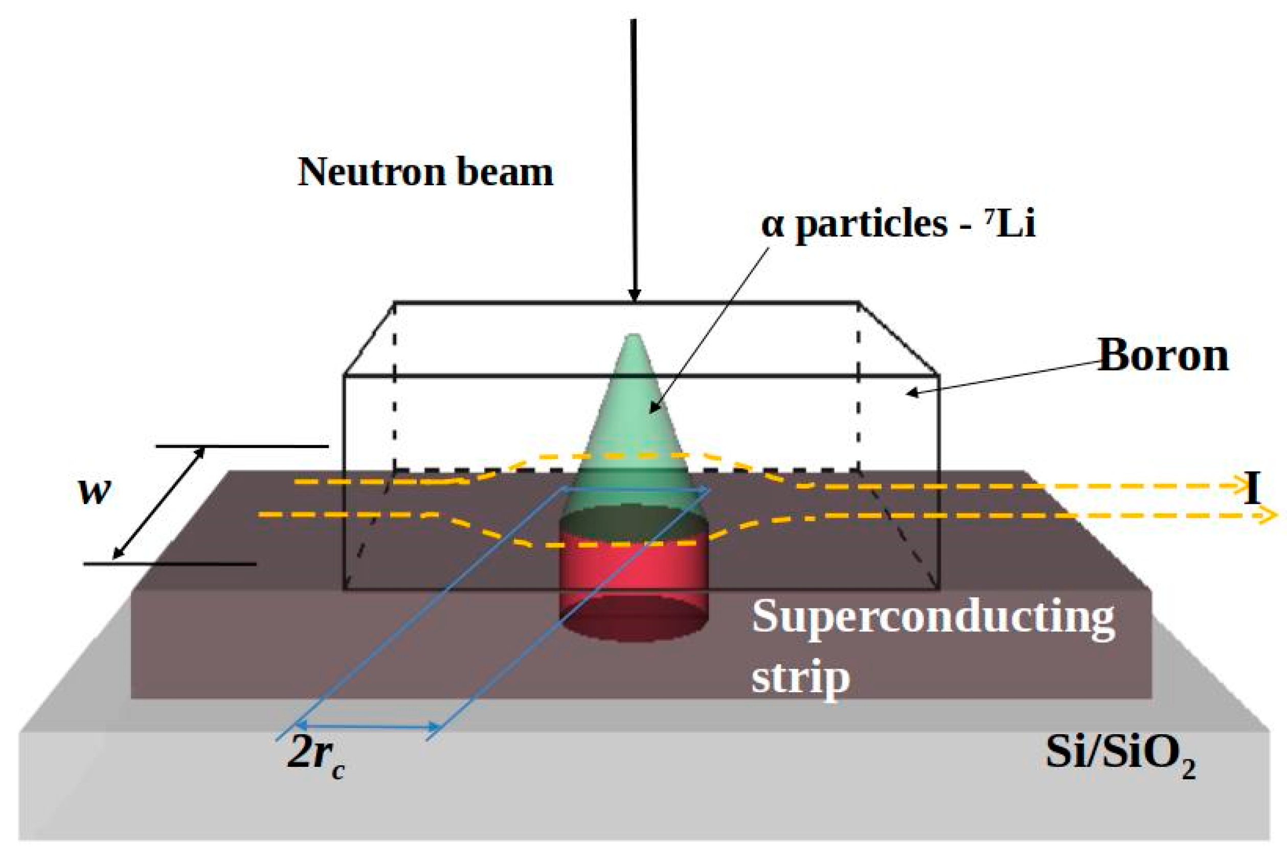
2. Basic Operating Principle and Related Physics
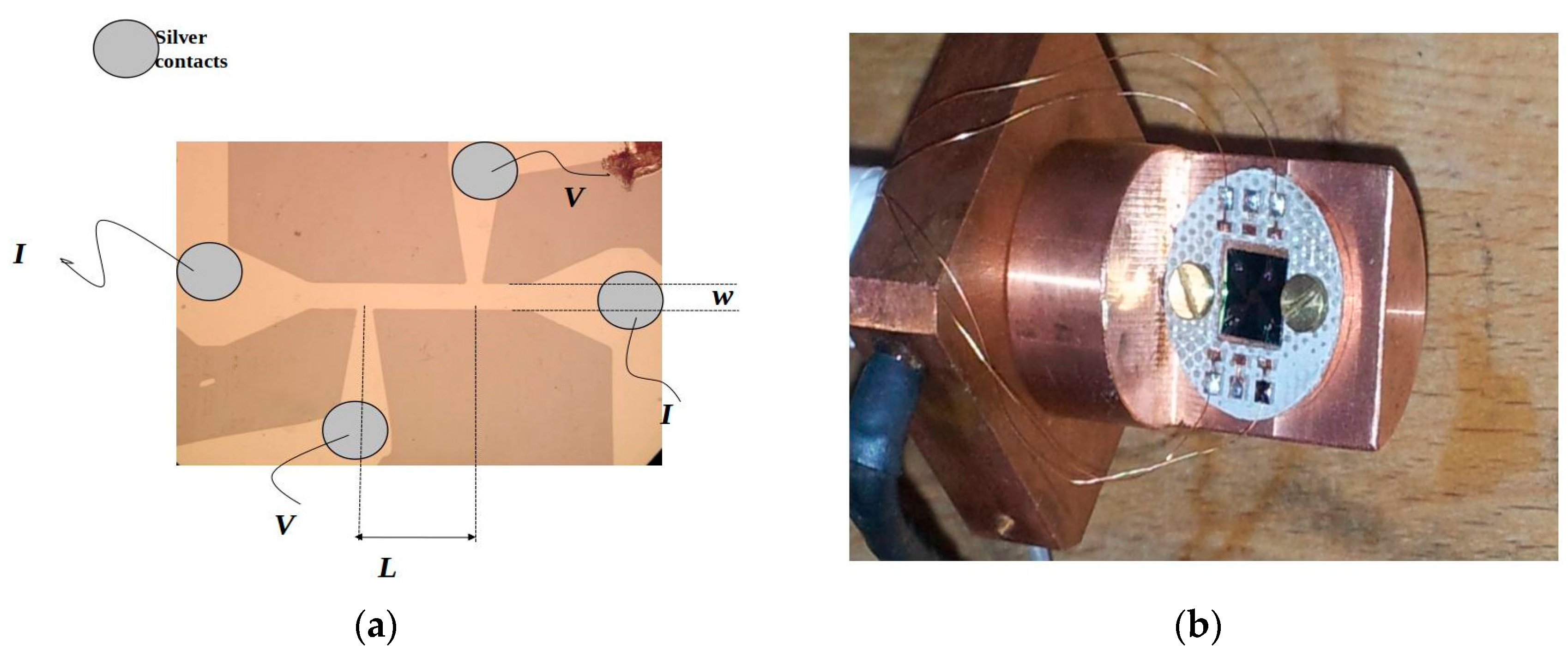
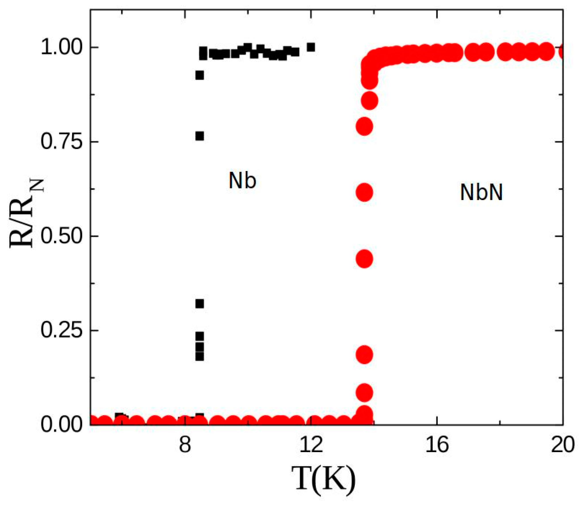
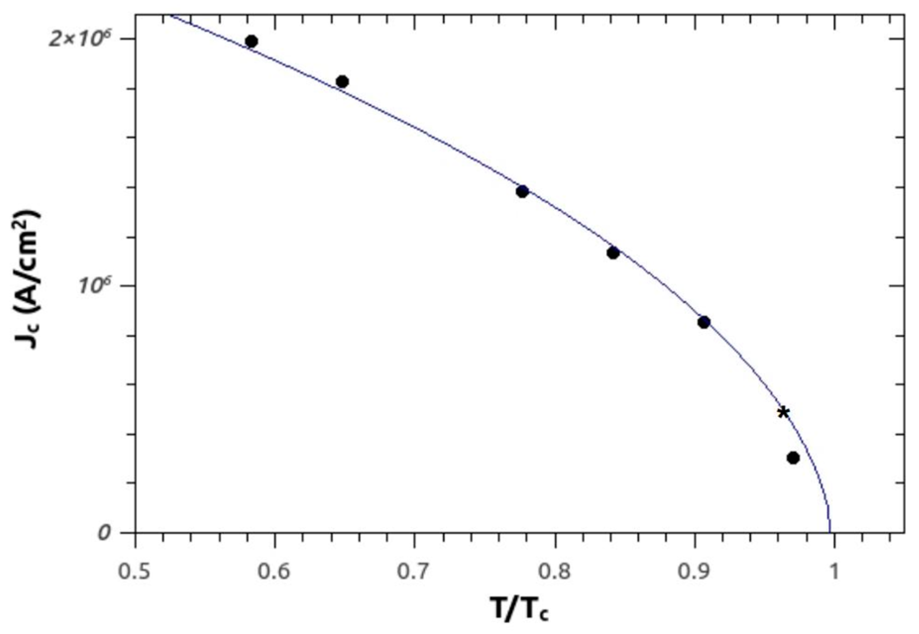
3. Sample Preparation and Characterization
4. Data Collection and Summary of Results
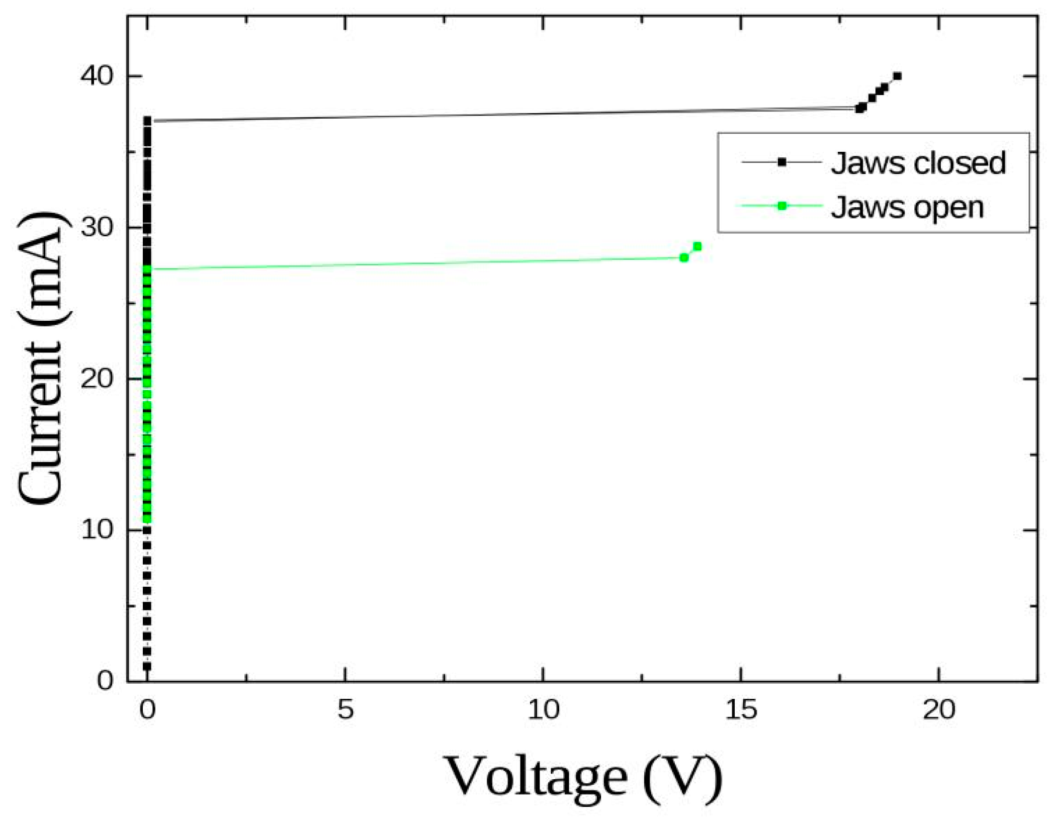
- Effect of contacts: in one set of measurements, electrical contact with the measurement apparatus was made by means of silver paint droplets on the contact pads. In principle, this can be a problem since Ag may become activated under thermal neutron irradiation with subsequent decay via charged products. To circumvent the problem, samples used in subsequent measurements were used where electrical contact was made via micro-bonding. Upon irradiation, no difference has been observed with previous measurements in the same experimental conditions, so the effect is deemed to be negligible and the bonding technique immaterial.
- Phonon decoupling: this has been most simply accomplished with the use of SiO2 on top of the substrates. This amorphous layer which is 1 µm thick seriously hinders phonon propagation from the crystalline Si back to the superconducting (sc) strip. It can be estimated that the phonon mean free path in the oxide is probably around 100 nm, although the value at low temperatures is strongly dependent on the film deposition technique. It should also be noted that boundary scattering from the interfaces could play a role in limiting the amount of heat transferred back to the sc strip. Crittenden [17] demonstrated that phonon decoupling takes place with just 30 nm of varnish deposited on the substrate.
- Blank measurements: in order to confirm the validity of our first set of measurements, data was also taken from irradiating a “naked” strip that is just Nb with no boron layer superimposed. Following the same procedure, no counts were recorded for times up to 30 min after starting the irradiation, thereby confirming that the boron layer is indeed responsible for neutron absorption and indirect detection.
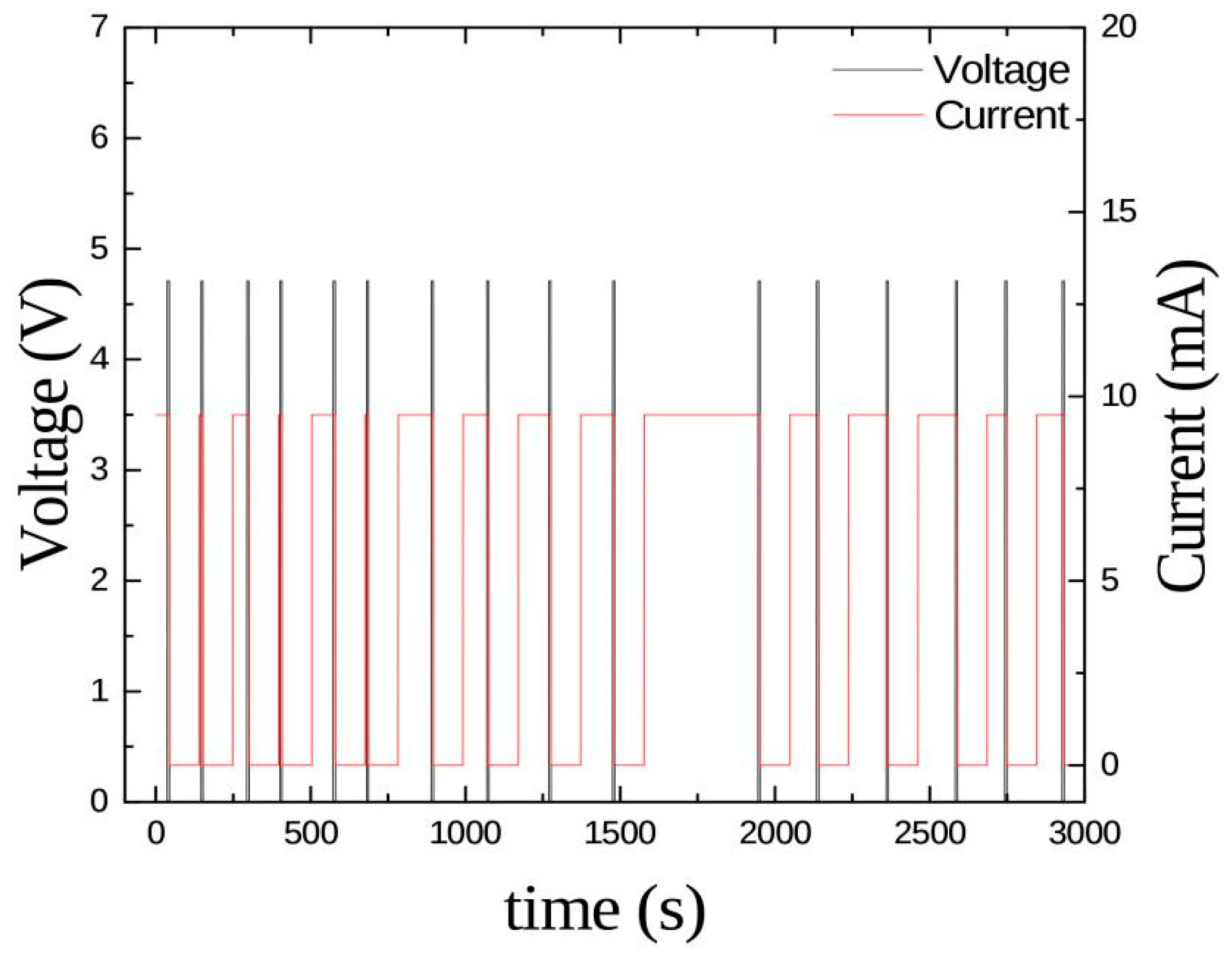
- With the experimental conditions described in P1 and P2 the expected count rate is in the order of 9 counts/min. This rate, which is quite low considering also the limited time available for irradiation, did not allow the performance any systematic study of the pulse shape and was barely sufficient to accumulate the statistics needed to demonstrate detector operation.
5. Conclusions and Overview
Acknowledgments
Conflicts of Interest
References
- Amaldi, E.; Fermi, E. On the absorption and diffusion of slow neutrons. Phys. Rev. 1936, 50, 899–928. [Google Scholar] [CrossRef]
- Rose, A. Sputtered Boron Films on Silicon Surface Barrier Detectors. Nucl. Instr. Methods 1967, 52, 166–170. [Google Scholar] [CrossRef]
- Almaviva, S.; Marinelli, M.; Milani, E.; Prestopino, G.; Tucciarone, A.; Verona, C.; Verona-Rinati, G.; Angelone, M.; Lattanzi, D.; Pillon, M.; et al. Thermal and fast neutron detection in chemical vapor deposition single-crystal diamond detectors. J. Appl. Phys. 2008, 103, 054501. [Google Scholar] [CrossRef]
- Petrillo, C.; Sacchetti, F.; Toker, O.; Rhodes, N.J. Solid State Neutron Detectors. Nucl. Instr. Methods 1996, 378, 541–551. [Google Scholar] [CrossRef]
- Caruso, A.N. The physics of solid state neutron detector materials and geometry. J. Phys. Condens. Matter 2010, 22, 443201. [Google Scholar] [CrossRef] [PubMed]
- McGregor, D.S.; Hammig, M.D.; Yang, Y.-H.; Gersch, H.K.; Klann, R.T. Design considerations for thin film coated semiconductor thermal neutron detectors. Nucl. Instr. Methods 2003, 500, 272–308. [Google Scholar] [CrossRef]
- Siegmund, O.H.W.; Vallerga, J.V.; Tremsin, A.V.; Feller, W.B. High Spatial and Temporal Resolution Neutron Imaging with Microchannel Plate Detectors. IEEE Trans. Nucl. Sci. 2009, 56, 1203–1209. [Google Scholar] [CrossRef]
- Gray, K.E. Non-equilibrium Superconductivity for Particle Detectors. In Proceedings of the International Workshop on Superconductive Particle Detectors, Torino, Italy, 26 October 1987; p. 1. [Google Scholar]
- Barone, A. Why Superconductive detectors? Nucl. Phys. B 1995, 44, 645–666. [Google Scholar] [CrossRef]
- Boot, N.E.; Goldie, D.J. Superconducting particle detectors. Supercond. Sci. Technol. 1996, 9, 493–516. [Google Scholar] [CrossRef]
- Merlo, V.; Salvato, M.; Cirillo, M.; Lucci, M.; Ottaviani, I.; Scherillo, A.; Celentano, G.; Pietropaolo, A. Hybrid superconducting neutron detectors. Appl. Phys. Lett. 2015, 106, 113502. [Google Scholar] [CrossRef]
- Merlo, V.; Salvato, M.; Lucci, M.; Ottaviani, I.; Cirillo, M.; Scherillo, A.; Schooneveld, E.M.; Vannozzi, A.; Celentano, G.; Pietropaolo, A. Meta-Material for nuclear particle detection. J. Phys. D Appl. Phys. 2017, 50, 045601. [Google Scholar] [CrossRef]
- Wagner, R.G.; Gray, K.E. Superconducting Thin Film Vertex Detector for SSC Applications. In Proceedings of the International Workshop on Superconductive Particle Detectors, Torino, Italy, 26 October 1987; p. 204. [Google Scholar]
- Andrews, D.H.; Fowler, R.D.; Williams, M.C. The Effect of Alpha-particles on a Superconductor. Phys. Rev. 1949, 76, 154. [Google Scholar] [CrossRef]
- Sherman, N.K. Superconducting Nuclear Particle Detector. Phys. Rev. Lett. 1962, 8, 438. [Google Scholar] [CrossRef]
- Spiel, D.E.; Boom, R.W.; Crittenden, E.C. Thermal Spikes in Superconducting Thin Films of Sn and In. Appl. Phys. Lett. 1965, 7, 292–294. [Google Scholar] [CrossRef]
- Crittenden, E.C.; Spiel, D.E. Superconducting Thin-Film Detector of Nuclear Particles. J. Appl. Phys. 1971, 42, 3182–3188. [Google Scholar] [CrossRef]
- Ziegler, J.F. Helium Stopping Power and Ranges in All Elements; Pergamon Press: New York, NY, USA, 1977. [Google Scholar]
- Skocpol, W.J.; Beasley, M.R.; Thinkam, M. Self-heating hotspots in superconducting thin-film microbridges. J. Appl. Phys. 1974, 45, 4054–4066. [Google Scholar] [CrossRef]
- Gray, K.E.; Kampwirth, R.T.; Zasadzinsky, J.F.; Ducharme, S.P. Thermal propagation and stability in superconducting films. J. Phys. F Met. Phys. 1983, 13, 405. [Google Scholar] [CrossRef]
- Wedenig, R.; Niinikoski, T.O.; Berglund, P.; Kyynäräinen, J.; Costa, L.; Valtonen, M.; Linna, R.; Salmi, J.; Seppä, H.; Suni, I. Superconducting NbN microstrip detectors. Nucl. Instr. Meth. 1999, 433, 646–663. [Google Scholar] [CrossRef]
- Cristiano, R.; Ejrnaes, M.; Casaburi, A.; Zen, N.; Ohkubo, N. Superconducting nano-strip particle detectors. Supercond. Sci. Technol. 2015, 28, 12404. [Google Scholar] [CrossRef]
- Ishida, T.; Nishikawa, M.; Fujita, Y.; Okayasu, S.; Katagiri, M.; Satoh, K.; Machida, M. Superconducting MgB2 thin film detector for neutrons. J. Low Temp. Phys. 2008, 151, 1074–1079. [Google Scholar] [CrossRef]
- Ishida, T.; Yoshioka, N.; Narukami, Y.; Shishido, H.; Miyajima, S.; Fujimaki, A.; Hidaka, M. Toward mega-pixel neutron imager using current-biased kinetic inductance detectors of Nb nanowires with 10B converter. J. Low Temp. Phys. 2014, 176, 216–221. [Google Scholar] [CrossRef]
- Ishida, T.; Miyajima, S.; Narukami, Y.; Yoshioka, N.; Shishido, H.; Hidaka, M.; Fujimaki, A. Toward neutron radiography using two arrays of Nb-based current-biased kinetic inductance detectors with 10B converter sandwiched in-between. IEEE Trans. Appl. Supercond. 2015, 25, 2401304. [Google Scholar] [CrossRef]
- Hoglund, C.; Birch, J.; Andersen, K.; Bigault, T.; Buffet, J.C.; Correa, J.; Khaplanov, A. B4C thin films for neutron detection. J. Appl. Phys. 2012, 111, 104908. [Google Scholar] [CrossRef]


© 2018 by the author. Licensee MDPI, Basel, Switzerland. This article is an open access article distributed under the terms and conditions of the Creative Commons Attribution (CC BY) license (http://creativecommons.org/licenses/by/4.0/).
Share and Cite
Merlo, V. Superconducting Strips: A Concept in Thermal Neutron Detection. Instruments 2018, 2, 4. https://doi.org/10.3390/instruments2010004
Merlo V. Superconducting Strips: A Concept in Thermal Neutron Detection. Instruments. 2018; 2(1):4. https://doi.org/10.3390/instruments2010004
Chicago/Turabian StyleMerlo, Vittorio. 2018. "Superconducting Strips: A Concept in Thermal Neutron Detection" Instruments 2, no. 1: 4. https://doi.org/10.3390/instruments2010004
APA StyleMerlo, V. (2018). Superconducting Strips: A Concept in Thermal Neutron Detection. Instruments, 2(1), 4. https://doi.org/10.3390/instruments2010004