

Article

Development of a Cherenkov-Based Time-of-Flight Detector Using Silicon Photomultipliers
1
Istituto Nazionale di Fisica Nucleare (INFN), Sezione di Bari, via Orabona 4, 70125 Bari, Italy
2
European Organization for Nuclear Research (CERN), Esplanade des Particules 1, 1211 Geneva, Switzerland
3
Dipartimento di Fisica dell’Università e del Politecnico di Bari, via Amendola 173, 70126 Bari, Italy
*
Authors to whom correspondence should be addressed.
Instruments 2026, 10(2), 28; https://doi.org/10.3390/instruments10020028
Submission received: 21 February 2026 / Revised: 17 April 2026 / Accepted: 27 April 2026 / Published: 13 May 2026

Abstract

The aim of this work is to develop high-precision time-of-flight (TOF) devices based on high-refractive-index solid Cherenkov radiators read out by silicon photomultipliers (SiPMs). Cherenkov light is prompt and, therefore, ideal for reaching the intrinsic timing limits of TOF systems. By utilizing a thin, high-refractive-index radiator, a nearly instantaneous signal is generated by particles exceeding the Cherenkov threshold. In order to achieve the ultimate time resolution, we carried out a rigorous optimization of the radiator material and geometry, alongside the efficiency of the optical coupling to the SiPM sensors. The key factors limiting the time resolution were characterized by comprehensive Monte Carlo simulations, subsequently validated against experimental beam test data. We assembled small-scale prototypes instrumented with various Hamamatsu SiPM array sensors with active areas ranging from 1.3 to 3 mm, coupled with various window materials, such as fused silica and MgF2, featuring various thickness values. The prototypes were successfully tested in beam test campaigns at the CERN-PS T10 beamline. The data were collected with a complete chain of front-end and readout electronics based on either the Petiroc 2A or the Radioroc 2 interfaced to a picoTDC to measure charges and times. By comparing the time measurements from two SiPM arrays, we were able to measure a time resolution better than 33.2 ps at the full system level, with a charged-particle detection efficiency of 100%. Our results demonstrate the expected performance benchmarks for the charged-particle detection efficiency and time resolution, and they highlight the potential of the developed Cherenkov-based TOF detectors for next-generation particle identification systems.

1. Introduction

The detection of Cherenkov radiation is a well-established technique for charged particle identification (PID) across broad momentum ranges, most notably in Ring-Imaging Cherenkov (RICH) detectors [1]. The generation of Cherenkov photons occurs when a charged particle traverses a medium with a refractive index n at a speed exceeding the phase velocity of light in the medium, β > 1 / n . Photons are promptly emitted (≈ps) along a cone with an opening angle θ C , defined by cos θ C = ( n ( λ ) β ) 1 .
The intrinsic promptness of the Cherenkov effect is also advantageous for applications in TOF devices. It has already been shown [2,3,4,5,6] that for charged particles traversing a radiator slab made of a high-refractive-index material, such as fused silica (SiO2), at a speed exceeding the threshold for Cherenkov emission, the resulting photons generate a fast, well-timed signal in photon sensors like Microchannel Plate Photomultipliers (MCP-PMTs).
A very promising photon-sensor alternative to MCP-PMTs for Cherenkov-based TOF devices is provided by silicon photomultipliers (SiPMs) due to their excellent key metrics. They include high intrinsic single-photon time resolution (SPTR) and photon detection efficiency (PDE) in the visible and near-ultraviolet (NUV) region of the spectrum, insensitivity to magnetic fields, and low material budget [7].
Previous studies have already investigated the use of SiPMs for the direct detection and timing of incident charged particles [8]. In such cases, the signals originate from Cherenkov photons emitted in the SiPM protective resin layer. However, these signals are typically confined to the single SiPM where the interaction occurs. This confinement, combined with the limited packaging factor of SiPMs in arrays, significantly reduces their overall efficiency for the direct detection of the impinging charged particles.
To overcome this limitation, we explored the approach of coupling a thin slab of transparent material (window) directly to a SiPM array, acting as a Cherenkov radiator for the incident charged particles, and resulting in clusters of contiguous fired SiPMs in the array. With a proper optimization of the radiator material and thickness, the geometry of the SiPM array, the optical couplings between the window and the SiPM array, and the front-end electronics, the proposed approach enables the achievement of time resolutions down to tens of ps, with a 100% charged-particle detection efficiency.
In this paper, we discuss the key factors affecting the time resolution and detection efficiency of the proposed approach by comparing the results obtained for various window materials and thicknesses, SiPM layouts, and off-the-shelf read-out electronic components. First, a comprehensive Monte Carlo simulation framework is presented, with emphasis on the interplay among radiator geometry, photon transport, and the intrinsic timing characteristics of the SiPMs. Subsequently, a characterization and optimization study of the SiPM anti-reflective coating is reported, aimed at quantifying and mitigating signal-photon losses induced by reflections within the relevant range of photon polarization, wavelength, and incidence angle of the impinging charged particles. Finally, the experimental setup of dedicated beam test campaigns is described, outlining the prototype architecture and benchmarking the measured performance against simulation results. This discussion highlights the impact of key detector parameters on the achieved overall time resolution, thereby establishing a reference for the development of next-generation Cherenkov-based timing systems for charged-particle identification.

2. Materials and Methods

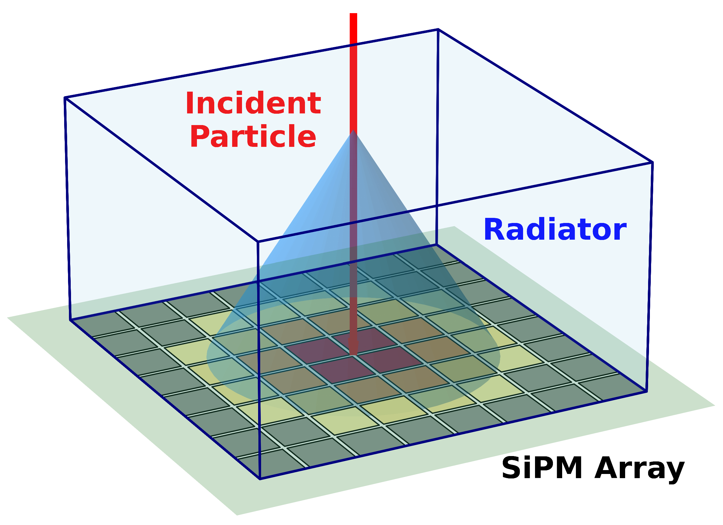
The principle of operation of the proposed Cherenkov-based timing approach is illustrated in Figure 1, showing the radiator coupled to the SiPM array and the Cherenkov cone from a charged particle traversing the radiator at a speed exceeding the threshold for Cherenkov emission. The emitted photons result in a localized cluster of hits in the array of SiPMs. The topology of these clusters, in terms of radius, average number of fired SiPMs, and distribution of photoelectrons, is determined by the slab refractive index, transmittance, and thickness, as well as by the SiPM granularity and PDE.
With a proper tuning of the radiator’s refractive index and thickness, the spatial extension of the Cherenkov cone effectively mitigates the impact of dead areas between adjacent SiPMs in the array and between the Single-Photon Avalanche Diodes (SPADs) in the same SiPM, ensuring a 100% detection efficiency across the entire sensitive surface.
The track timing is then obtained by combining the timestamps of the SiPMs in the cluster. The precision of each individual measurement is determined by the intrinsic resolution of the SiPMs and the contributions of the electronics jitter, the time-to-digital converter (TDC) resolution, and the time reference system. This method offers two advantages:
  • In the cluster core, where many photoelectrons are expected, the pixel with maximum charge yields the best intrinsic time resolution and the lowest time jitter.
  • By combining the timestamps of those SiPMs in the cluster core with a sufficiently high number of photoelectrons, the overall time precision could be further improved.
As a result, track time resolutions at the level of a few tens of ps can be achieved.

2.1. Candidate Radiator Materials

The choice of the radiator material is primarily driven by the particle species and the momentum range of interest for TOF measurements, typically requiring high detection efficiency down to the lowest possible momenta. In the proposed Cherenkov-based timing approach, this requirement is primarily addressed by minimizing the Cherenkov emission threshold for the different particle species, ensuring that particles reach Cherenkov angle saturation at the lowest possible momenta, while maximizing the emission angle.
For a particle with mass m, the momentum threshold in a material with refractive index n is p th = m / n 2 1 . Materials with high refractive indices are characterized by low momentum thresholds p th , large Cherenkov emission angles θ c , and high photon yields N ph , which scale as N ph sin 2 θ c , thus leading to large clusters.
Possible materials for the sensor entrance window are NaF ( n 1.33 ), MgF2 ( n 1.38 ), and SiO2 ( n 1.47 ). These materials provide excellent NUV transparency, good radiation hardness, and favorable optical coupling to common SiPM protective coatings, typically made of either silicone ( n 1.41 ) or epoxy ( n 1.55 ) resins, using a thin layer (<100 μ m) of optical grease or adhesive for gluing the window to the SiPM array. The quoted refractive index values are reported at a wavelength of 400 nm. For radiators based on these materials, the Cherenkov emission threshold is below 1 GeV / c for protons, and substantially lower for lighter species.
The choice of SiO2 as radiator material is particularly convenient due to several key features. First, because it allows for a precise control of the thickness over the radiator surface, which is a critical parameter in tuning the Cherenkov cone geometry and cluster size on the SiPM array. Moreover, its excellent radiation hardness ensures stable performance even in the high-luminosity environments typical of modern particle accelerators, preventing the degradation of transparency.
Although materials with n > 1.6 enable Cherenkov emission by particles with lower momenta than those traversing fused silica radiators, their use for this application has several drawbacks. The optical coupling to the SiPM is more challenging due to the large mismatch of the refractive indices at the various interfaces. The resulting effects are a severe loss of photons because of the multiple reflections and a larger background from photons undergoing total internal reflections.

2.2. Contributions to the Time Resolution

The total time resolution at the single-SiPM level results from the convolution of several physical and instrumental contributions, including the Cherenkov emission process, signal formation in the SiPMs, and the response of the electronics [9,10]:
σ t 2 = σ geom 2 + σ SiPM 2 + σ FE 2 + σ TDC 2
  • Geometric Spread, σ geom : Photons travel different paths from the emission point to the sensor. For a radiator of thickness d and normally incident charged particles, the maximum time spread is Δ t max = d ( β 2 n 2 1 ) / β c , leading to a contribution to the resolution σ geom d / 12 . This term also accounts for the chromatic dispersion of the radiator in the spectral region to which the SiPMs are sensitive, with the wavelength dependence of n ( λ ) broadening the arrival time distribution.
  • Intrinsic SiPM Jitter, σ SiPM : This contribution originates from the stochastic nature of photoelectron creation, charge multiplication [11], and the spread in the charge transit time across multiple SPADs. For SiPMs with a given SPTR, the intrinsic time resolution depends on the number of photoelectrons N PE as σ SiPM SPTR / N PE 1 / d . Both the SPTR and N PE improve with the increasing operating overvoltage. Moreover, SPTR depends on the total capacitance of the SiPM, which is proportional to the area of the photosensitive part of the SiPM and the number of SPADs.
  • Front-End Jitter, σ FE : This term accounts for the time uncertainty introduced by the front-end electronics in the timestamp reconstruction. It is primarily driven by the electronic noise and by the finite signal rise time: noise causes fluctuations in the time pick-off (e.g., threshold crossing), and the effect is larger when the signal slope at the pick-off point is smaller. Since the signal amplitude and slope scale with the collected charge, this contribution scales approximately as σ FE 1 / N PE 1 / d . The σ FE decreases with increasing pre-amplifier gain and decreasing discriminator threshold.
  • TDC Quantization Uncertainty, σ TDC : This term accounts for the finite time binning of the TDC. Assuming a uniform quantization error within one bin, the corresponding contribution is σ TDC = LSB / 12 , where LSB is the least significant bit.
While a thinner radiator minimizes the geometric spread ( σ geom d ), it reduces the N PE , resulting in a degradation of the σ SiPM and σ FE . Additional instrumental contributions, such as the finite precision of the reference time ( t 0 ) and the clock stability, can also broaden the measured time distributions and, therefore, affect the overall resolution.
When the Cherenkov photons emitted in the radiator fire more SiPMs in the array, N SiPM , the independent measurement of the time for each SiPM would enable an improvement of the time resolution, ideally by a factor 1 / N SiPM . However, when combining the timestamps from several SiPMs with different values of N PE , time-walk effects introduced by leading-edge discrimination must be corrected, since signals with smaller amplitude exhibit a reduced slew rate and, therefore, cross the discriminator threshold at a later time, biasing the measured timestamp. After applying the time-walk correction, the particle’s time of arrival can be estimated as the average of the corrected timestamps measured by the SiPMs in the cluster.

2.3. Monte Carlo Simulation Optimization Studies

We implemented a comprehensive Monte Carlo simulation for design optimization studies. This section illustrates the results obtained assuming SiO2 [12] as the radiator material for ultra-relativistic ( β 1 ) particles at normal incidence. We generated Cherenkov photons in the wavelength interval from 260 to 900 nm using the Frank–Tamm formula (Equation 34.44 of Ref. [13]). The PDE of Hamamatsu S13360 SiPMs [14] and an SPTR of 100 ps were assumed for the sensors in the array. Pixel sizes of 1.3 × 1.3 mm2, 2 × 2 mm2, and 3 × 3 mm2, with a 200 μ m gap between each pixel, were considered. SPAD pitches of 50 μ m and 75 μ m were assumed, corresponding to a PDE of 40% and 50%, respectively, at a wavelength of 450 nm for operation at an overvoltage of 3 V. The contribution from the readout chain, σ FE , σ TDC , and other instrumental effects was modeled as σ ele = 50 ps / N PE 20 ps .
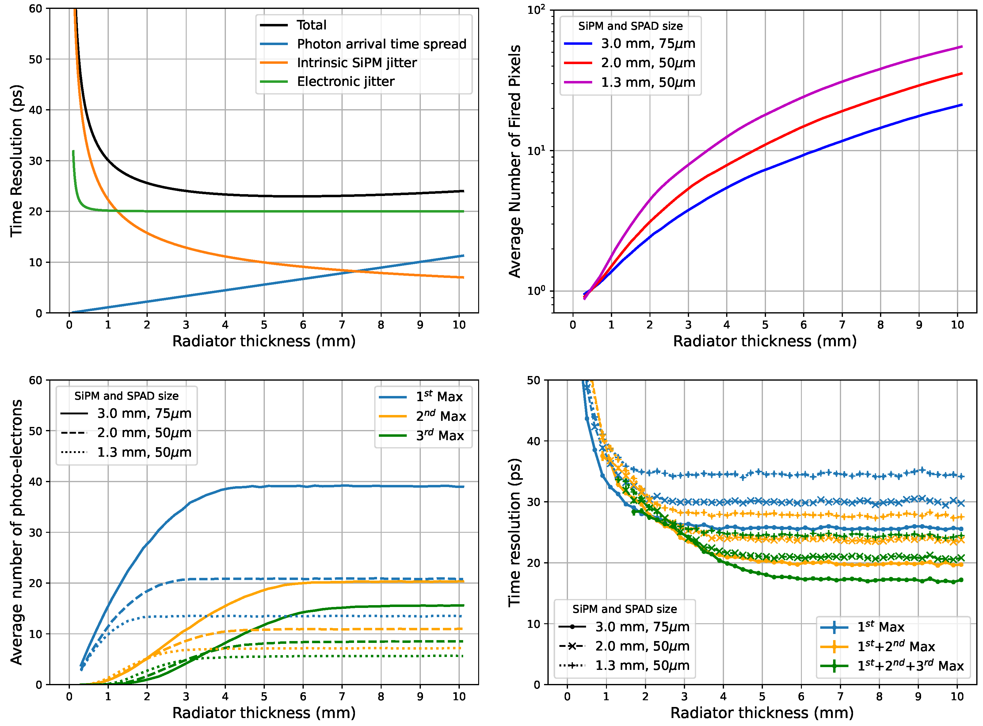
The top-left panel of Figure 2 presents the total time resolution and the individual contributions as a function of radiator thickness, including the geometric spread, intrinsic SiPM jitter, and the contribution of the electronics. The calculation assumes an infinitely extended SiPM active area for the collection of photons and a SPAD pitch of 75 μ m . This dependence highlights the intrinsic design trade-off: reducing the radiator thickness decreases the geometric time spread ( σ geom d ) yet simultaneously lowers the number of detected photons, thereby worsening the photoelectron statistics term ( σ SiPM 1 / d ) and increasing the N PE -dependent electronic jitter.
The top-right panel of Figure 2 reports the average number of fired pixels as a function of radiator thickness for the SiPM technologies under consideration, accounting for the actual SiPM size for photon collection. The bottom-left panel of Figure 2 shows the corresponding average number of photoelectrons collected in the three pixels with the highest signal amplitude. The bottom-right panel of Figure 2 presents the resulting total time resolution, obtained by averaging the photon-arrival times from those three pixels. The results indicate that a total time resolution better than 40 ps can be achieved for radiator thicknesses of d 1 mm with the SiPM devices and electronic parameters considered in this study. It is worth noting that the ultimate performance is limited by the timing capabilities of the readout electronics implemented in the simulation.

2.4. Photon Reflections at the SiPM Interface

Photon reflections at the interface between the SiPM and the radiator have an impact on the overall PDE, which directly influences the number of produced photoelectrons, generating fluctuations in the photo-statistics and, therefore, in the timing resolution. At the same time, photons reflected by a SiPM might reach and be detected by farther SiPMs, potentially resulting in delayed and displaced background hits.
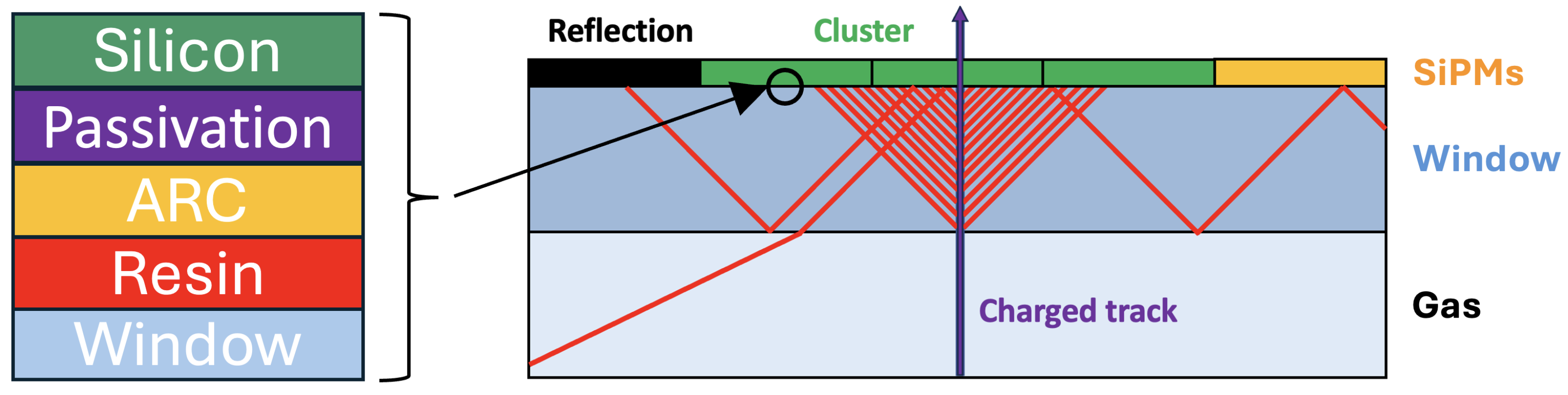
Fresnel reflections arise at the interfaces between the environmental gas in the expansion gap, the sensor window, and the successive layers of the SiPM structure, including the protective resin, the anti-reflective coating (ARC), the passivation layer, and silicon, as illustrated in Figure 3. Diffuse reflections are also expected because of the microstructures on the SiPM surface, such as quenching resistors, trenches and traces used to connect the SPADs, as well as from regions between adjacent SiPMs in the array [15]. Although the background from reflected photons can be suppressed by operating at a sufficiently high threshold, optimizing the optical coupling between the radiator window and the SiPM array could enhance the detection of the Cherenkov photons.
Since little information regarding the layout and material composition of ARCs is available from the SiPM vendors, to characterize the SiPM reflectance, we performed dedicated measurements with commercial arrays featuring various pixel pitches and active areas, as well as various protective resins and radiator materials. We measured the corresponding total, diffuse and specular reflectance. In addition, we developed a simple model (Appendix A) to explain and compare the various contributions to the measurement results. Using this model, we also extrapolated the wavelength dependence of the reflectance resulting from the built-in ARC of the SiPMs in the tested arrays.
The specifications of the tested arrays for reflectance measurements are summarized in Table 1.
The tested arrays included four 8 × 8 Hamamatsu S13361 series arrays with SiPMs of 3 × 3 mm2 in area, featuring a pixel pitch of 50 µm or 75 µm and a protective layer made of epoxy resin or silicone resin. On top of the arrays with silicone resin, a 1 mm thick SiO2 window or a glass with a refractive index of 1.84 at 400 nm, hereafter referred to as high-n glass, was glued. An additional 2 × 2 mm2 array with epoxy resin and a 50 µm SPAD pitch was also tested [16]. The corresponding fill factor (FF), defined as the fraction of active area in a SiPM, and the integration factor (IF), corresponding to the fraction of the array area covered by SiPMs, are also reported in Table 1.
Reflectance measurements were performed using an Agilent 900 External Diffuse Reflectance Accessory (DRA) integrating sphere [17] coupled with an Agilent Cary 4000 UV-Vis spectrophotometer [18]. For each array, we performed direct measurements of the total reflectance R tot and diffuse reflectance R diff in the wavelength range from 200 to 800 nm, in steps of 1 nm, at an 8° incidence angle. We then extrapolated the corresponding specular reflectance R spec as follows:
R spec = R tot R diff .
We assigned an uncertainty of 0.05% to the measured R tot and R diff , and an additional factor of 2 , resulting from error propagation, to R spec . The results are reported in Section 3.1.

2.5. Beam Test Measurement Campaigns

We carried out a series of dedicated beam test campaigns at the CERN-PS T10 beamline [19] to validate the proposed charged-particle timing approach. The primary goal was the characterization of the topology of the Cherenkov clusters produced by charged particles, along with the evaluation of the efficiency and time resolution of a complete SiPM–electronics chain.

2.5.1. Tested SiPM Arrays

Following the simulation studies discussed in Section 2.3, we tested 8 × 8 Hamamatsu S13361 SiPM arrays featuring various pixel sizes (1.3 mm, 2.0 mm, and 3.0 mm) and pixel pitches (1.5 mm, 2.2 mm, and 3.2 mm), as well as two different protective resins (epoxy and silicone) with a thickness of about 100 μ m.
The SiPMs were optically coupled to windows made of either SiO2 or MgF2, with nominal thicknesses of 1 mm or 2 mm. The S13361–3075 arrays equipped with 1 mm thick SiO2 or MgF2 windows were purchased directly from Hamamatsu with the pre-bonded optical window. Conversely, the 2 mm thick SiO2 windows were bonded in-house using EJ-500 optical cement [20]. Measurements with bare arrays were also performed for comparison. In this work, we focus on the results obtained with the arrays reported in Table 2.
All of the measurements reported below were performed with the T10 negatively charged beam at 10 GeV/c momentum. The beam composition consisted of approximately 95% pions, 3% electrons, and 2% kaons [19]. For the radiator materials considered in this work, all of the beam particle species were in the Cherenkov angle saturation regime.

2.5.2. The SiPM Array Telescope

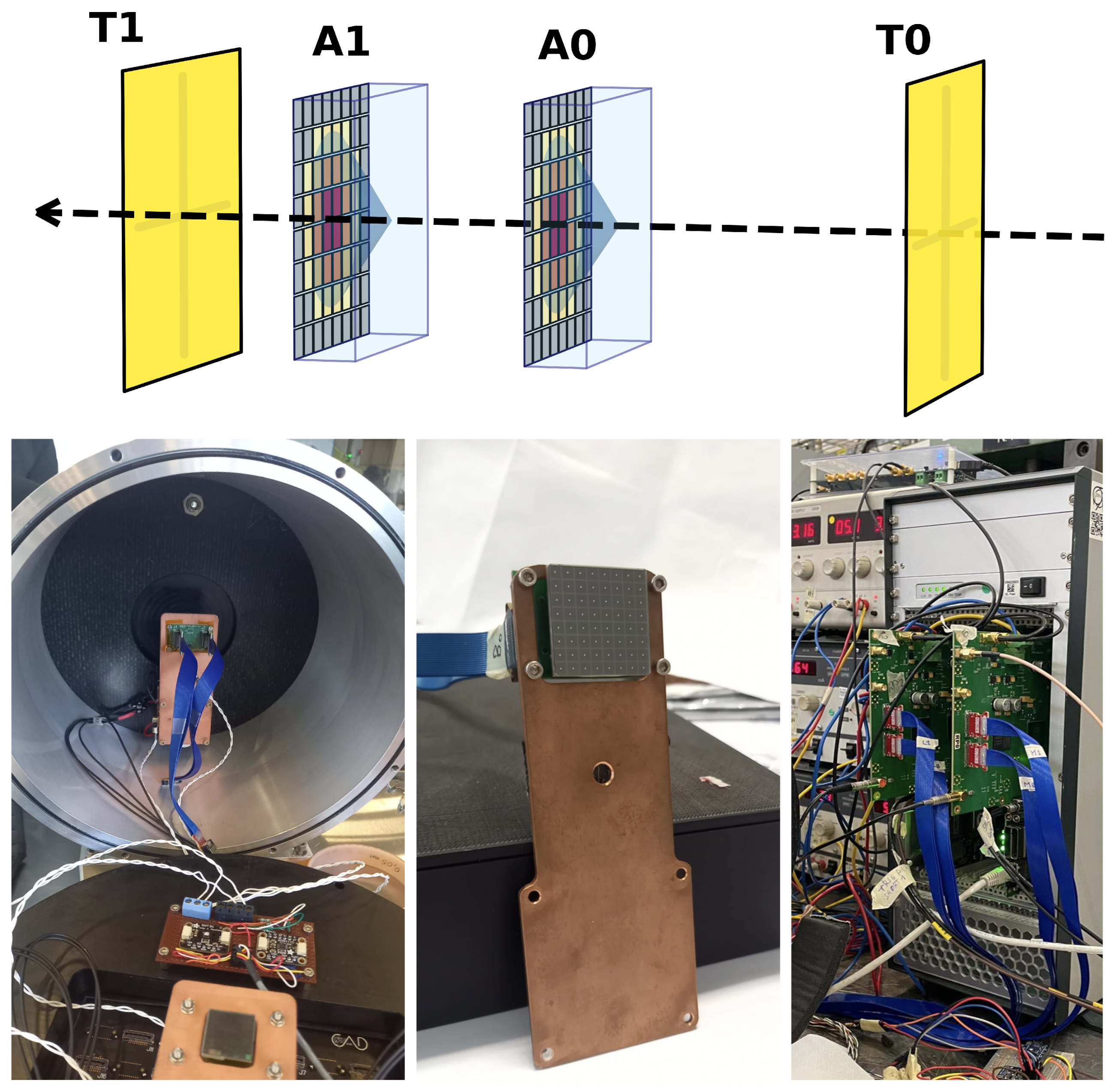
The setup is illustrated in Figure 4. A telescope of four detectors arranged along the beamline was used. We consider a reference frame in which X and Y are the horizontal and vertical coordinates, respectively, in the plane transverse to the beam, while the Z coordinate is defined along the beam direction. Two X-Y tracker modules, hereafter denoted as T0 and T1, based on staggered round plastic scintillating fibers coupled with Hamamatsu S13552 128-channel SiPM arrays [21], were mounted upstream and downstream of the SiPM arrays at a distance of about 125 cm for triggering and tracking purposes [22,23,24]. Two SiPM arrays, hereafter referred to as A0 and A1, both facing the beam, were mounted inside a cylindrical vessel placed between the tracker modules, at a separation of about 28 cm, with A0 located upstream of A1. We tested various combinations of the arrays listed in Table 2. This enabled the characterization of the timing performance by comparing the times of arrival measured by the A0 and A1 arrays, using one of the two as a reference time for the other.

2.5.3. SiPM Cooling and Temperature Monitoring

To ensure mechanical stability and efficient thermal management, the SiPM arrays were mounted on custom-designed printed circuit boards (carrier boards), which were fixed to copper baseplates. The SiPMs were cooled down to 0 °C through a dedicated cooling system incorporating water chillers and Peltier cells coupled to the baseplates to reduce the SiPM dark count rate (DCR). The temperatures of the baseplates and the carrier boards were monitored using TT4-10KC3-T125-M5-500 analog temperature sensors [25] assembled on the edges of the baseplates and read out using a Raspberry Pi 3 [26] with ADS1115 16-bit ADCs [27], and with 1-wire DS18B20 digital temperature sensors [28] mounted on each carrier board, respectively. The temperature remained stable, with maximum observed fluctuations of about 1 °C throughout all runs and for all tested configurations. The vessel was flushed with argon gas to reduce the humidity and maintain dew point values well below the minimum operating temperature inside the vessel, thereby preventing condensation. SHT31-D humidity sensors [29] were used to monitor both the ambient and vessel humidity.

2.5.4. Cabling of the SiPMs to the Front-End

All SiPM arrays were bonded on one side of the carrier board, routing the channels to Samtec LSHM–120 multi-channel connectors [30] bonded on the opposite side of the carrier board. The 128 channels of each S13552 array of T0 and T1 were arranged into 32 groups (OR4), each consisting of four adjacent channels, resulting in a readout pitch of 1 × 1.625 mm2. Each of those groups of channels was routed to a single LSHM–120 multi-channel connector. The S13361 arrays inside the vessel were instead plugged with their Samtec ST4–40 [31] connectors to different carrier boards equipped with Samtec SS4–40 [32] connectors, and all channels were routed to two LSHM–120 multi-channel connectors, each handling 32 channels. For the arrays reading the views of T0 and T1, the Samtec LSHM–120 multi-channel connectors were connected directly to the front-end boards (FEBs) by means of high-speed 50 Ω multi-channel Samtec HLCD–20 cables [33]. For A0 and A1, the Samtec LSHM–120 multi-channel connectors were first connected to a feed-through PCB connector using Samtec HLCD–20 cables, and then an additional cable was plugged for each array to route the analog signals from the feed-through PCB connector to the FEBs placed outside. The SiPM bias voltage was provided through four of the HLCD channels by CAEN A7585D bias modules [34]. A HLCD channel was dedicated to the readout of the 1-wire digital temperature sensor.

2.5.5. SiPM Readout Electronics

We tested two different front-end architectures for the A0 and A1 arrays—one based on the Petiroc 2A ASIC [35], and one based on the Radioroc 2 ASIC [36] coupled with the picoTDC [37]—in order to assess the contribution of the electronics to the overall time resolution. The SiPMs were interfaced to the front-end electronics through custom FEBs, hereafter referred to as the Petiroc board and the RadioPico board. The arrays reading the X and Y views of T0 and T1 were connected to two different Petiroc FEBs for all of the measurements reported in this work. In contrast, the A0 and A1 arrays were read out by the same Petiroc FEB for measurements performed with the Petiroc 2A, and by two RadioPico FEBs for measurements performed with the Radioroc 2 and picoTDC.
The Petiroc Board
The Petiroc board, developed by the Electronics Workshop of the INFN unit of Bari, is equipped with four Petiroc 2A ASICs developed by Omega-Weeroc [35]. The Petiroc 2A is a 32-channel ASIC providing per-channel arrival time and charge readout. Each channel integrates a 10-bit analog-to-digital converter (ADC) for charge measurement and a 10-bit time-to-digital converter (TDC) with 40 ps LSB for timing. A nominal time jitter smaller than 150 ps FWHM is expected for more than two PE signals for operation at a 0.5 PE threshold (ASIC only). Four LSHM–120 Samtec connectors are used to route the analog SiPM signals to each ASIC. Besides the front-end ASICs, the Petiroc board hosts a CAEN A7585D SiPM voltage supply module [34] to bias the SiPMs and a Kintex–7 FPGA mounted on a Mercury+ KX2 module [38]. The board and DAQ infrastructure is based on the MOSAIC system [39]. There are six NIM input and output lines dedicated to external trigger operation and synchronous multi-board operation. Further details can be found in [22].
The RadioPico Board
The RadioPico board is equipped with one Radioroc 2 ASIC, developed by Weeroc [40], coupled with one picoTDC ASIC [41], developed by CERN, connected to a MOSAIC readout board [39]. The ASICs have 64 channels, allowing the readout of a 8 × 8 SiPM array with each board. Two LSHM–120 Samtec multi-channel connectors are used to route 32 SiPMs each to the Radioroc 2. The signals entering the Radioroc 2 are fed to the time pre-amplifier and discriminated by setting a threshold. The ASIC is configured to provide a differential digital output signal for each input channel, with an expected jitter as low as 35 ps FWHM on a single PE (ASIC only). This signal is fed as input to the picoTDC, working with a 40 MHz differential clock provided through dedicated SMA connectors by an external Skyworks SI5341-D-EVB differential clock board [42], enabling an LSB as low as 3.05 ps. The picoTDC is operated in ToT mode, allowing the measurement of both the time of arrival (ToA) and the time over threshold (ToT), serving as a proxy for the charge. For each external trigger, hits detected within a programmable time window and matched to the trigger with a programmable latency are acquired by the MOSAIC board. External bias to the SiPMs is provided by a CAEN A7585D module through an additional LEMO connector on the mezzanine.

2.5.6. Overvoltage and Threshold

In our measurements, the S13361 SiPMs exhibited an average breakdown voltage of approximately 52 V at 25 °C, with a maximum channel-to-channel variation of ±0.1 V and a temperature coefficient of about 54 mV/°C. Since the Petiroc 2A and Radioroc 2 ASICs provide only per-channel fine trimming of the bias, the temperature-dependent variation of the overvoltage is compensated by adjusting the global HV offset through the external supply module (CAEN A7585D). This configuration ensures stable overvoltage conditions and uniform gain across all channels over the full operating temperature range.
Data were collected at various overvoltages and discriminator thresholds. The results reported below refer to configurations in which the arrays were operated at an overvoltage of about 6 V for all tested A0 and A1 combinations, with the thresholds set as described below. For acquisitions with the Petiroc board, the threshold was set to approximately three PEs for all S13361 arrays equipped with a window, and between one and two PEs for arrays without a window. For acquisitions with the RadioPico board, the threshold was set to one PE for all tested configurations. At the considered overvoltage of 6 V and a temperature of 0 °C, the measured DCR was between 20 and 30 kHz/mm2 for arrays with a 50 μ m SPAD pitch and between 30 and 45 kHz/mm2 for arrays with a 75 μ m SPAD pitch at the single-PE level. When the threshold was set to three PEs, the DCR was reduced to less than 0.1 kHz/mm2 for all arrays.

2.5.7. Event Selection

The signals from the fiber tracker were used for external triggering. The trigger was then distributed to the other Petiroc and RadioPico boards. We selected events requiring that the SiPM channels with the maximum charge observed in both the X and Y views of T0 and T1 had at least six photoelectrons. We also required the times of those channels to be within an 8 ns window to suppress the background due to wrong or ghost hits in multi-particle events. In addition, after a standard alignment procedure based on the minimization of the residuals, only events with tracker hits within fiducial regions defined according to the SiPM sizes of the A0 and A1 arrays were considered. These regions were chosen to ensure that the particle traversed both arrays.

2.5.8. Charge and Time Calibration

For the arrays read out with the Petiroc board, a 550 ns data-acquisition time window was opened for each trigger event. Within this window, the system recorded the fired channels together with their corresponding ADC and TDC measurements. Charge calibration was performed starting from the measured ADC counts. For each event, we evaluated the actual ADC counts of individual channels by subtracting the corresponding pedestal values. We identified the peaks in the ADC charge distribution corresponding to each number of photoelectrons. Then, we calculated the ADC-to-PEs calibration constants [24]. Time calibration was subsequently performed. The hit time-of-arrival in the Petiroc 2A ASIC was determined in two steps. A coarse-time (CT) counter with a 40 MHz clock was used as a reference and digitized with a 9-bit counter. A ramp-based Time-to-Amplitude Converter (TAC) was used to interpolate the fine time (FT) between two coarse time edges and digitized with a 10-bit counter. For each Petiroc 2A channel, the discriminator output was used as a start for the TAC ramp, which was stopped by the following edge of the 40 MHz coarse-counter clock signal. Based on the shape of the measured CT and FT distributions, hCT and hFT, we reconstructed the time information t(ns) as follows:
t ( ns ) = P 40 × CT + 1 i = 0 FT h FT ( i ) / i = 0 1023 h FT ( i )
where P 40 = 25 ns is the period of the reference 40 MHz clock.
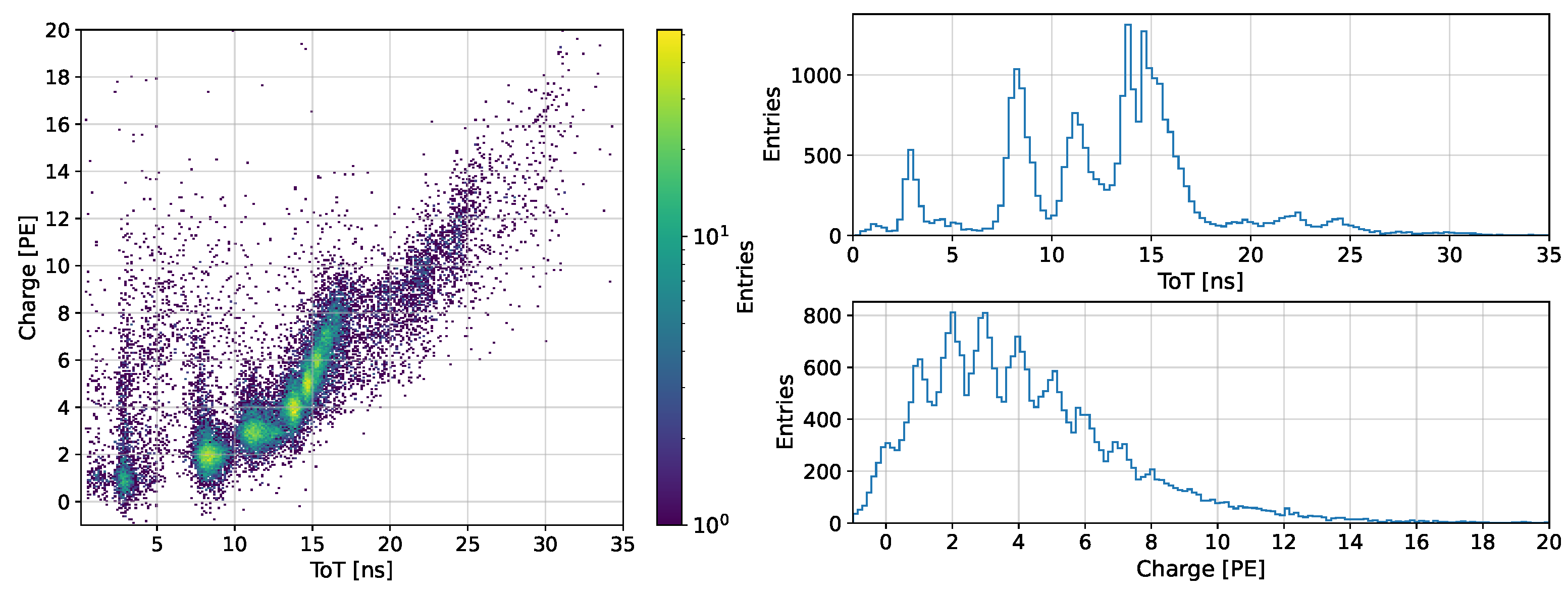
For the arrays read out with the RadioPico board, the Radioroc 2 time pre-amplifier was configured to operate at its maximum gain, while picoTDC was configured with a ToA LSB of 3.05 ps and a ToT LSB of 195 ps to achieve the best time resolution. Data acquisition was performed in triggered mode with a 200 ns acquisition window, and the ToA was measured relative to an external trigger. Upon each trigger, with a programmable latency, all digital hits recorded by the picoTDC in the acquisition window were read out by the FEB–MOSAIC system, allowing multiple hits per channel within a single event. The ToA and ToT values were computed from the corresponding ToA and ToT counters, implemented with 16-bit and 11-bit resolution, respectively, assuming the nominal ToA and ToT LSB values. Although the ToT provides a proxy for the deposited charge, the relationship between ToT and number of PEs is not linear and does not exhibit a strictly monotonic one-to-one correspondence. Figure 5 shows the charge distribution measured with an oscilloscope and the corresponding ToT distributions for the same set of events acquired under laser illumination. This is particularly important for defining accurate time-walk corrections, especially when pixels with a small charge are used to calculate some cluster parameters, such as the average timing. For this reason, the cluster analyses reported in this work were mainly performed using Petiroc data, while the RadioPico analysis was limited to SiPMs with the maximum ToT.

3. Results

3.1. SiPM Reflectance Measurements and ARC Optimization Studies

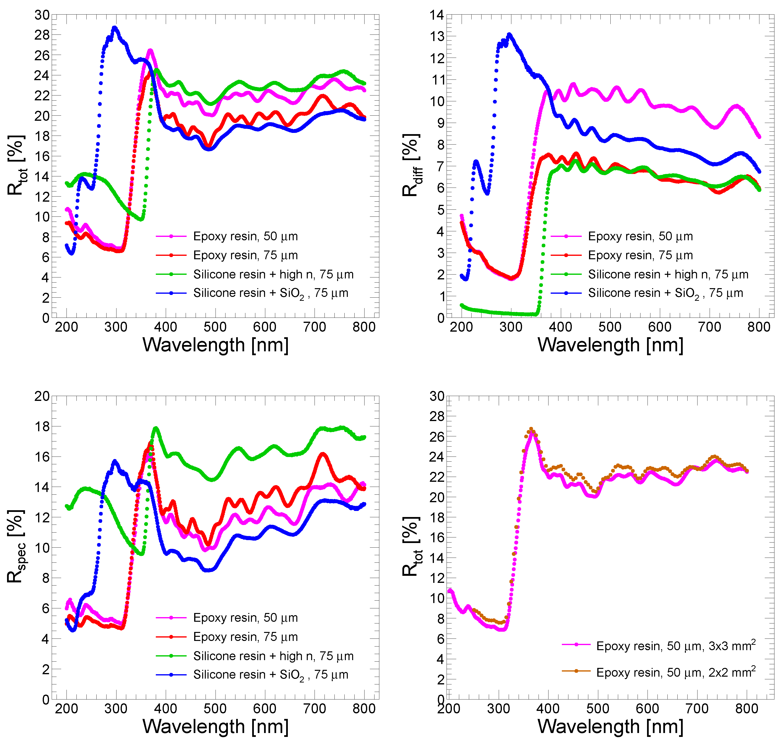
The measured total, diffuse, and specular reflectance values as a function of wavelength for the arrays in Table 1 are shown in Figure 6. The following features can be highlighted. Oscillation structures were observed for all tested SiPMs. These are mainly generated by thin-film interference effects at the upper and lower boundaries of the ARC stacks, as thin as about tens of nm, on the surfaces of the SiPMs [15]. Since the protective layers and the additional entrance windows are much larger than the wavelengths of the incident light—about 100 μ m and 1 mm, respectively—their contributions to the oscillations are negligible. The total reflectance values are between 18% and 24% for wavelengths larger than 380 nm for all tested arrays. These include the contributions of a diffuse reflectance between 6% and 10% and a specular reflectance between 8% and 18%. For wavelengths below 380 nm, the reflectance curves of the tested arrays drop sharply due to the absorption in the protective layer or, when present, in the SiPM entrance window. The pronounced cutoffs at 380 nm, 360 nm, and 280 nm correspond to regions where absorption becomes dominant in high-n glass, epoxy resin, and silicone resin, respectively. In contrast, the SiO2 window is expected to cut off at shorter wavelengths, outside the range of interest.
The two arrays with epoxy resin and pitches of 50 µm exhibit similar specular reflectance curves. However, the total reflectance is higher for the 50 µm SPAD arrays because the lower FF increases the diffuse contribution to about 10%, compared with about 7% for the 75 µm arrays. The slight difference in reflectance between the two arrays with 2 × 2 mm 2 and 3 × 3 mm 2 SiPMs, both mounting epoxy resin and using 50 μ m SPADs, is consistent with the different IFs of the SiPMs in the arrays, as reported in Table 1.
The array coupled to the SiO2 window using silicone resin shows the lowest cutoff, at about 280 nm, which is driven by absorption in silicone resin. This array also shows the lowest total reflectance values at wavelengths larger than 380 nm. In particular, it exhibits the lowest specular reflectance and a diffuse reflectance no larger than 1% with respect to the other tested arrays. This array thus presents optimal features for TOF applications.
The array coupled to the high-n glass shows the highest total and specular reflectance due to stronger Fresnel reflections upon entrance, with about 9% probability, driven by the larger refractive index difference between air and the high-n material. Conversely, the coupling of SiO2 windows to either silicone or epoxy resins presents a smaller refractive index difference, which leads to lower reflectance (about 4%) at the air interface. For the same reason, the observed diffuse reflectance for the high-n glass array is smaller than for the other arrays, since a significantly larger fraction is already reflected specularly upon entrance and, therefore, does not even reach the surface microstructures that generate diffuse contributions. Given these characteristics, this array is not optimal for the proposed TOF application.
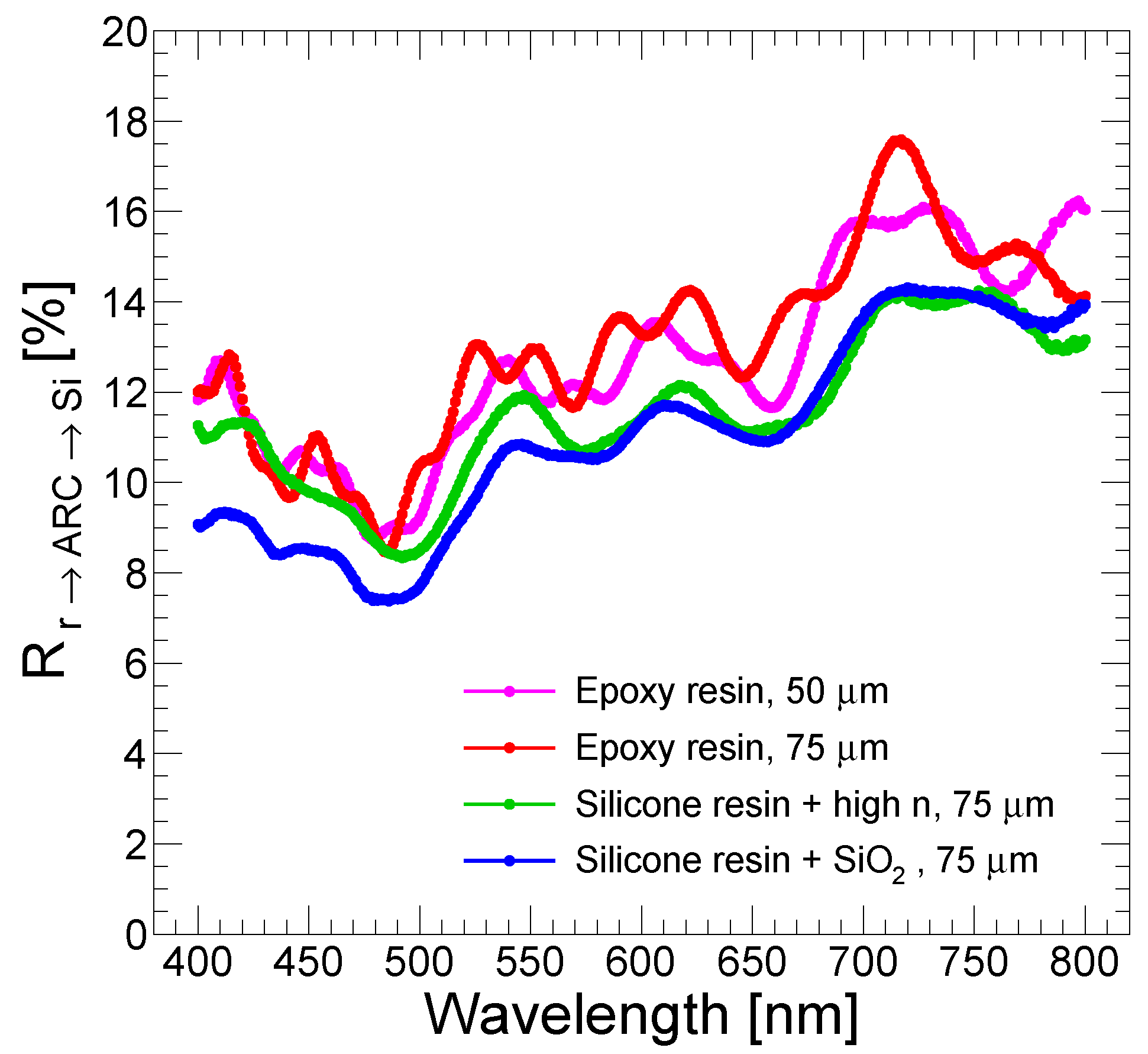
Using the SiPM reflection model reported in Appendix A, from the measured specular reflectance of the tested arrays, we extrapolated the overall reflectance resulting from the interfaces between the SiPM protective resin and ARC, between the ARC and passivation layer, and between the passivation layer and silicon R r ARC Si . In particular, using the IF and FF values in Table 1, together with the nominal refractive indices of SiO2, high-n glass, silicone resin, and epoxy resin, we extracted the R r ARC Si curves shown in Figure 7 for wavelengths larger than 400 nm at an 8° incidence angle.
Across all tested SiPM arrays, the extrapolated specular reflectance at the ARC interface fell in the range of 8–14%. The measured R r ARC Si includes both the intrinsic properties of the ARC and the contribution of the resin, which cannot be separated on the basis of the available data. In particular, as expected, the extrapolated curves in Figure 7 group into two families: blue and green for silicone resin, and magenta and red for epoxy resin. Coupling with silicone resin yields a systematically lower reflectance by about 2% relative to epoxy resin. This reduces interface losses at the considered 8° incidence angle. However, it is not known whether the silicone and epoxy variants employ the same ARC, and differences in the ARC design cannot be excluded. Nevertheless, the agreement of the curves within each resin family, independent of the window material or its absence, together with the differing FF values across arrays, provides additional validation of the proposed reflection model.
Although the tested commercial SiPMs demonstrated optimal reflectance at the interfaces with the built-in ARC, even lower reflectance values could be achieved by optimizing the ARC accounting for the wavelength-dependent Cherenkov spectrum, scaling as d N / d λ λ 2 ; the polarization of Cherenkov photons, featuring inherent polarization perpendicular to the surface of the cone; and the SiPM spectral response. In this way, it is possible to maximize photon collection over the relevant photon incidence-angle distributions by reducing reflections and increasing the effective SiPM PDE.
We developed an advanced simulation tool to optimize an arbitrary N-layer SiPM ARC, based on the polarization-dependent transfer matrix formalism for thin films (see Chapter 10 of [43]). The tool accounted for the upstream window material and SiPM protective resin, as well as for the downstream passivation layer and silicon. To include absorption in silicon and other materials, we used the general formalism with a complex refractive index, n ˜ = n + i κ , where n is the usual refractive index and κ is the extinction coefficient. The ARC affects reflection through thin-film interference. For layers with thickness greater than the photon wavelength, such as the 100 μ m thick typical resin layers or the mm thick windows, coherence is lost, and the corresponding contribution to the reflectance is averaged over the photon propagation phase.
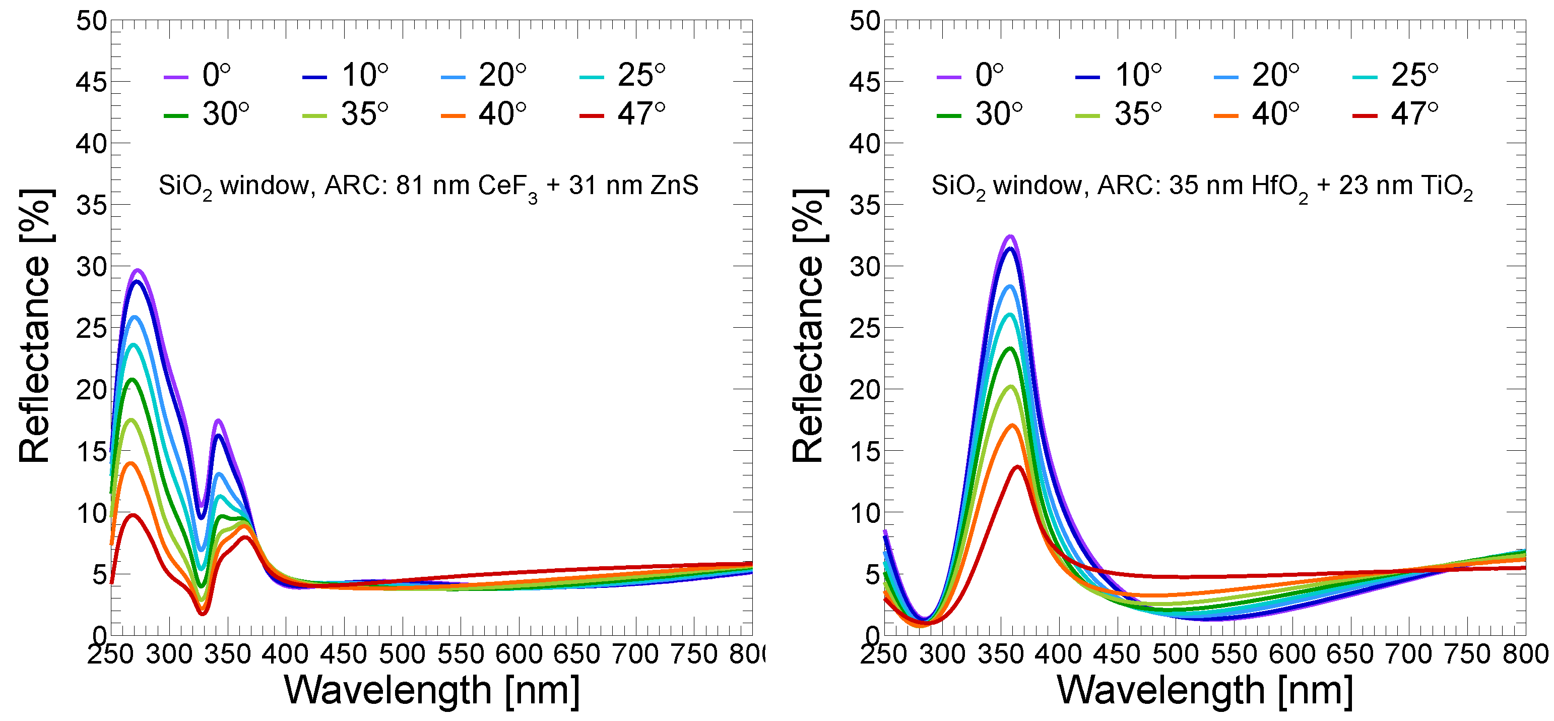
Figure 8 shows the overall reflectance for two examples of a two-layer ARC aimed at maximizing the overall number of detected photons for normally incident tracks at saturation, assuming a 1 mm thick SiO2 window, a 100 μ m thick silicone resin protective layer, and a 10 nm thick SiO2 passivation layer. We optimized the thicknesses of the ARC layers assuming the spectral response of Hamamatsu S13360–3075CS SiPMs [14]. In particular, the left panel shows the results for an ARC made of an 81 nm thick layer of CeF3 [44] and a 31 nm thick layer of ZnS [45], while the right panel shows the results for a two-layer ARC made of a 35 nm thick layer of HfO2 [46] and a 23 nm layer of TiO2 [47]. Together with the reflectance curve at the saturated Cherenkov emission angle in SiO2 ( θ C 47 ), the curves corresponding to lower photon emission angles with the expected polarization (P-polarization) are also shown to illustrate the effect expected for photons emitted by charged particles in the regime between the Cherenkov threshold and saturation.
Reflectance values of about 5% were obtained with the considered ARCs throughout the wavelength region of interest. Even lower reflectances are expected with more complex ARCs. Compared with the values in Figure 7, these simulations indicate that custom ARCs tailored to the specific application discussed in this work could, in principle, reduce the overall reflectance by approximately a factor of two with respect to commercial ARCs.

3.2. Window Cluster Topology and Charge

For a given combination of A0 and A1, we studied the topology of the clusters resulting from the detection of the Cherenkov photons produced by the impinging charged particles.
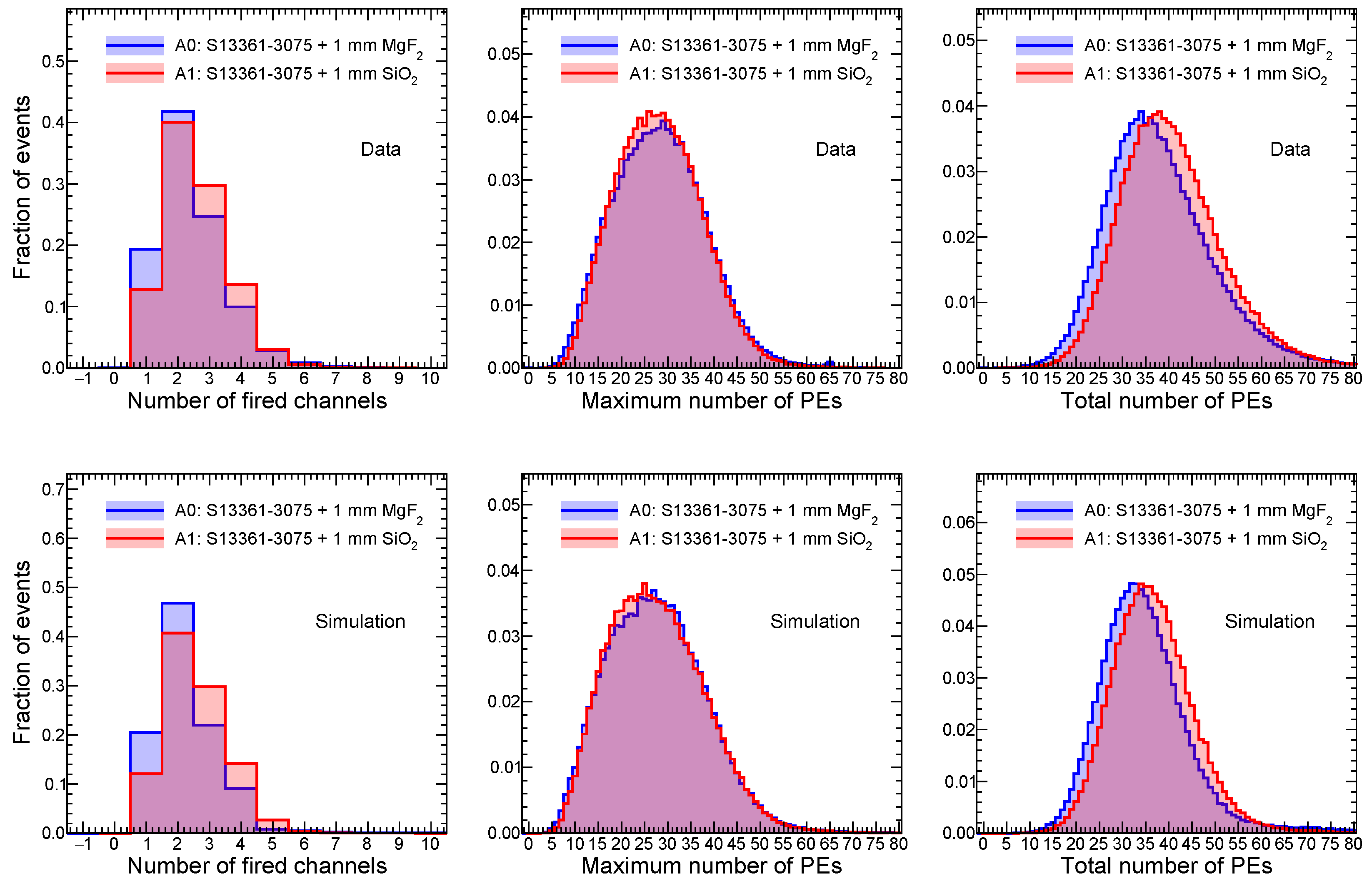
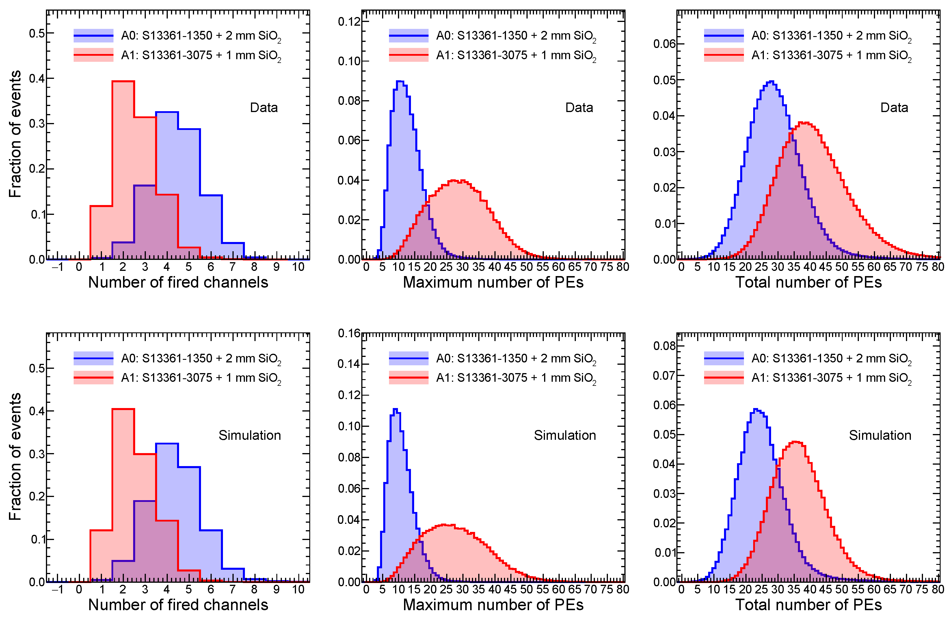
The top panels of Figure 9 and Figure 10 show the measured number of fired channels, the maximum number of photoelectrons in a single SiPM in the clusters, and the total number of photoelectrons in the clusters for two different configurations tested with the Petiroc boards. In both cases, the same S13361–3075 array coupled with a 1 mm thick SiO2 window was used as A1. The S13361–3075 array coupled with a 1 mm thick MgF2 window and the S13361–1350 array coupled with a 2 mm thick SiO2 window, respectively, were used as A0.
The bottom panels of the same figures show the corresponding expectations from the full simulation of the setup in the Geant4 framework [48,49,50]. The simulation includes a detailed description of the relevant processes, such as optical transport with reflections, the production and propagation of secondary particles, and the response of the SiPMs in terms of DCR, PDE, and cross-talk. For the dark count rate, we used the measured values. For the PDE and the cross-talk probability, we assumed the nominal PDE as a function of photon wavelength and the nominal cross-talk probability at the operating overvoltage [14]. In addition, the simulation also accounted for the emission of Cherenkov photons by electrons and pions at 10 GeV/c momentum in the argon circulated through the vessel. Overall, the data were reasonably well reproduced by the simulation.
Under the considered operating conditions in terms of overvoltage and threshold, the arrays equipped with 3 × 3 mm2 SiPMs with 75 μ m SPAD pitch exhibit on average 2–3 fired channels per cluster, with a mean maximum charge of about 30 PEs and a mean total charge of 35–40 PEs for 1 mm thick SiO2 and MgF2 windows. As expected, the arrays with SiO2 and MgF2 windows exhibit very similar behavior, given their very close refractive indices and optical transparency. The slight excess observed with SiO2 in terms of number of fired channels and total charge is mostly attributable to the detection of extra Cherenkov photons emitted by 10 GeV/c pions and electrons in the Ar volume at angles smaller than 1 . 5 ° . In particular, simulations show that about 4–5 Cherenkov photons from the 28 cm Ar region between the two arrays are detected on average in A1, compared to about 1 detected photon on average in A0 from the 8 cm gap between the vessel entrance and A0.
Despite the 3 PE threshold for the 3 × 3 mm2 SiPM arrays, about 3% of the events recorded with 1 mm thick windows exhibit clusters with five or six fired channels. If only direct signal photons emitted in the window contributed, no more than four channels would be above the threshold. This excess is well reproduced by the simulation once additional contributions are included, namely, photons undergoing multiple reflections before detection, photons produced in the Ar volume (distributed over a cone with a radius of about 7 mm at A1 and 2 mm at A0), and correlated background from secondary particles. In addition, optical cross-talk generates correlated photoelectrons that can lift otherwise sub-threshold cells above threshold, enhancing the observed channel multiplicity to the observed values.
For the array with 1.3 × 1.3 mm2 SiPMs with 50 μ m SPAD pitch and a 2 mm thick SiO2 window, about 4–5 channels are fired, with a mean maximum charge of 10–11 PEs and a total charge of about 23–24 PEs, indicating significantly larger charge-sharing, as expected from the smaller pixel size. Although these values are consistent with the expected larger charge-sharing for a thicker window and a smaller SiPM active area, the total charge might appear low when compared to the 1 mm window case, since a 2 mm window is expected to produce approximately twice as many photons. This difference can be understood by accounting for the lower fill factor and PDE of the 50 μ m SPAD pitch case with respect to the 75 μ m case, the reduced geometric acceptance of the 1.3 × 1.3 mm2 active area relative to the 1.5 × 1.5 mm2 SiPM pitch compared to the 3 × 3 mm2 active area with 3.2 × 3.2 mm2 pitch, the smaller cross-talk probability [14], and the reduced contribution from Ar photons in A0. A significant contribution also arises from the different optical transmittance of the protective resins of the arrays, as highlighted in Section 3.1. The epoxy resin of the S13361–1350 array absorbs photons with wavelengths shorter than about 360 nm, whereas the silicone resin of the S13361–3075 array exhibits high transmittance down to about 280 nm. Finally, the finer segmentation distributes the photons over more channels with a smaller charge per channel, increasing the probability that some channels fall below the 3 PE threshold and do not contribute to the measured total charge. When all of these effects are included, the measured values are consistent with expectations, as validated by simulation.
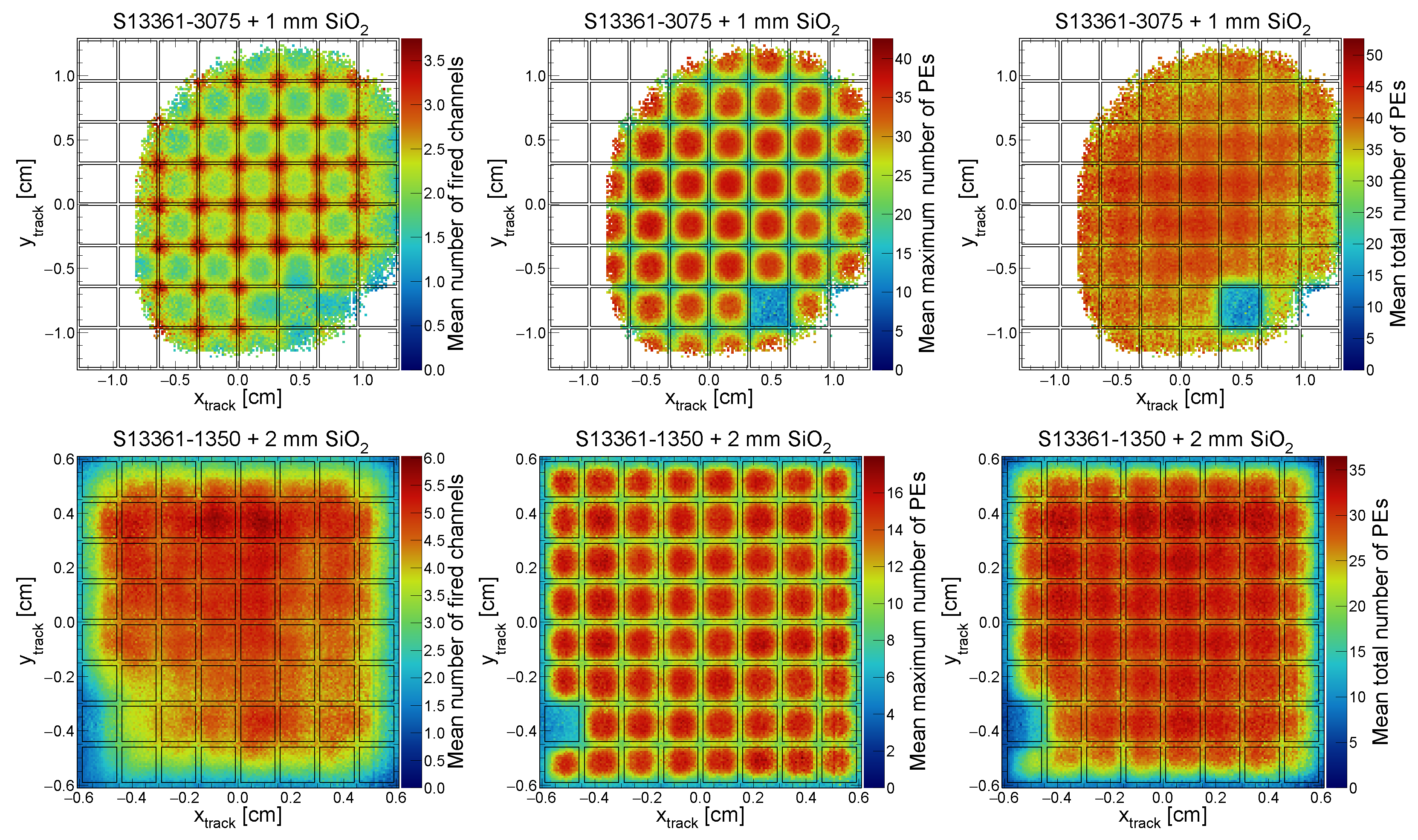
Figure 11 shows the mean number of fired channels in the clusters, the mean maximum charge in a single SiPM, and the mean total number of photoelectrons in the charged track clusters measured with the Petiroc boards as a function of the track impact point ( x track , y track ) for the S13361–3075 array coupled with a 1 mm thick SiO2 window (top panels) and the S13361–1350 array coupled with a 2 mm thick SiO2 window (bottom panels). Because of the presence of dead channels in the two arrays, we excluded the regions corresponding to those channels from the timing analysis.
The maps of the number of fired channels and of the cluster charge highlight how the available photoelectrons are shared among neighboring SiPMs. For the S13361–3075 configuration, multi-channel clusters are predominantly observed when the track crosses boundaries between adjacent SiPMs. For the S13361–1350 configuration, instead, multiple channels are fired over the full impact region, reflecting the finer segmentation and the additional lateral spread induced by the thicker window. As expected, in both cases, the mean total charge is approximately uniform across the array.
The maps of the mean maximum charge show that the largest values are reached for tracks incident near the center of a SiPM, with a mean maximum of up to about 40 PEs for the S13361–3075 array and about 17 PEs for the S13361–1350 array, as expected from considerations of the geometry. Approaching the SiPM boundaries, the maximum observed charge decreases, and the same charge is shared more equally among the neighboring SiPMs. This is crucial for the timing performance achieved by taking into account only the SiPM with maximum charge, or averaging the contributions of multiple SiPMs, as discussed in detail in Section 3.4.
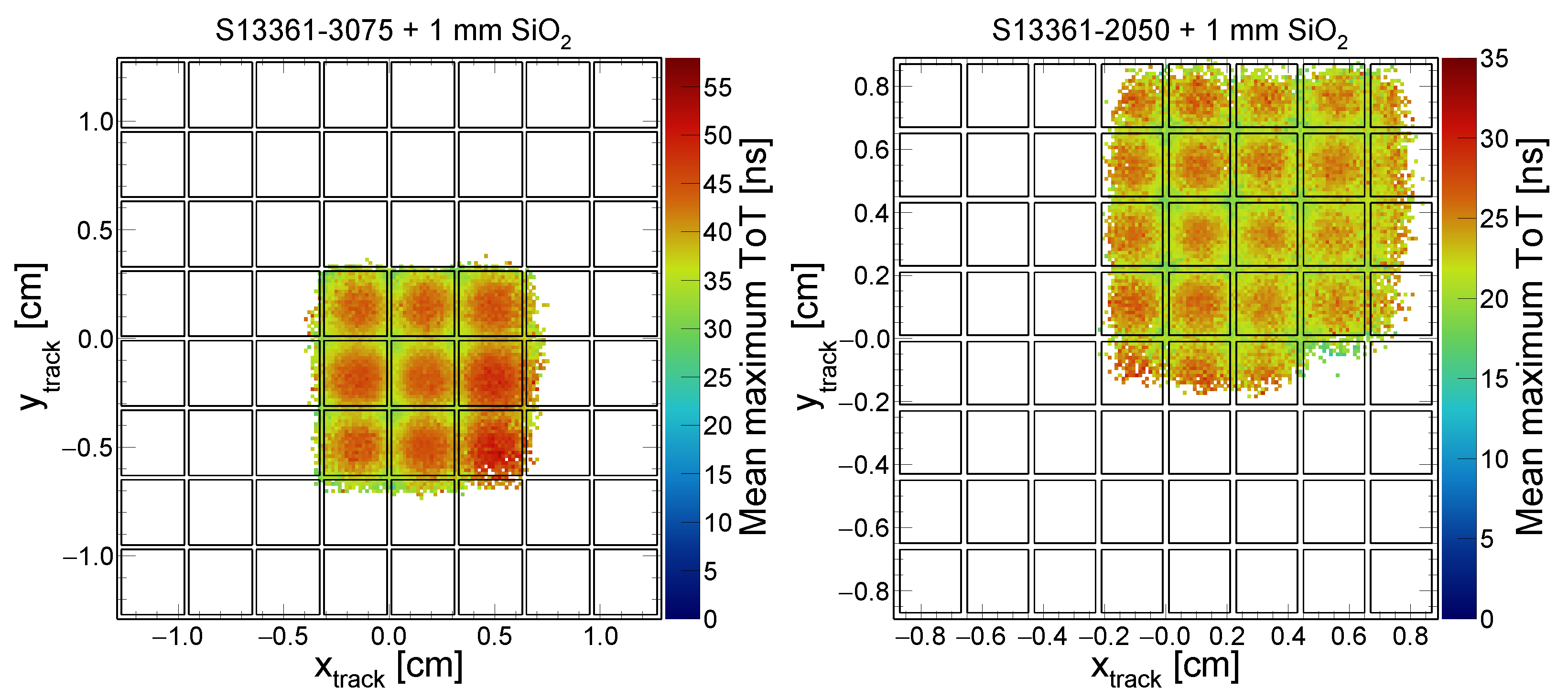
To compare the response of the Petiroc board with that of the RadioPico board, Figure 12 shows the maps of the mean maximum ToT in the charged track clusters measured with the RadioPico boards as a function of the track impact point ( x track , y track ) for the S13361–3075 array coupled with a 1 mm thick SiO2 window (left panel) and the S13361–2050 array coupled with a 1 mm thick SiO2 window (right panel). The displacement of the beam spot centers in the two arrays, by about 1 mm in X and 4 mm in Y, is due to a slight offset of the two arrays relative to the nominal beam position. The observed maps follow those of the maximum charge, with a mean maximum ToT of about 45–50 ns for the S13361–3075 array and 25–30 ns for the S13361–2050 array close to the center of the SiPMs. Therefore, we considered the channel with the maximum ToT in the cluster as a reference for the characterization of the timing performance with the RadioPico boards.

3.3. Charged-Particle Detection Efficiency

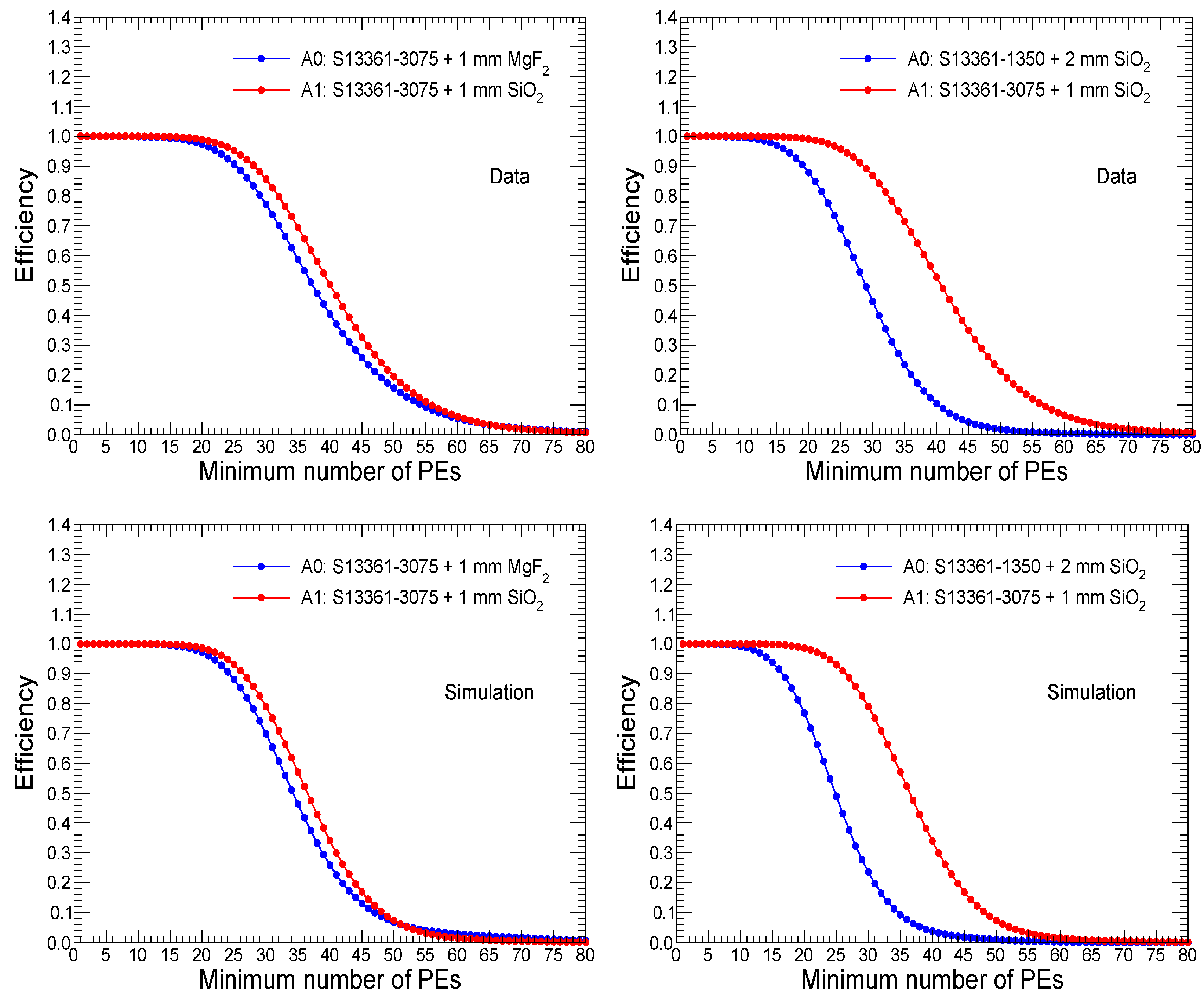
For a given combination of A0 and A1, we evaluated the efficiency of A0 (A1) as the 4-fold/3-fold coincidence ratio, defined as the fraction of events with signals in both tracker planes and in A1 (A0) for which a cluster in the array under study met or exceeded the required minimum number of PEs. The left panels of Figure 13 show the measured and the simulated efficiency as a function of the minimum number of PEs required in the clusters for runs taken using Petiroc boards for the configuration with the S13361–3075 array coupled with a 1 mm thick SiO2 window (A1) and the S13361–3075 array coupled with a 1 mm thick MgF2 window (A0). The right panels of the same figure show the corresponding results with the S13361–1350 array coupled with a 2 mm thick SiO2 window used as A0.
We found efficiency values above 99.9% when requiring up to 14 and 7 PEs in the clusters of the S13361–3075 and S13361–1350 arrays, respectively, and above 99% when requiring up to 20 and 12 PEs, respectively. We found intermediate values for tests with the S13361–2050 arrays. The measured values are consistent with the simulation predictions and directly follow from the considerations reported in Section 3.2.
These results demonstrate the high efficiency of the adopted timing strategy, while allowing operation at threshold values that can suppress the background from the SiPM DCR even in very high-radiation environments. This approach is therefore a solid option for timing applications in future high-energy physics experiments, where radiation tolerance is a primary requirement.

3.4. Time Resolution

We performed timing studies by comparing the ToAs measured by the A0 and A1 arrays, using one of the two as a reference time for the other. We corrected the raw time differences for channel-by-channel time offsets, due to the different routing of the channels, and the time-walk effect, accounting for signals with the same shape but increasing amplitudes systematically crossing the discriminator threshold at earlier times. We subtracted the global time-of-flight offset as well. We determined all of the required corrections in a single step, using dedicated calibration runs and a lookup-table procedure. In particular, for data taken with the Petiroc boards, we built, for each combination of A0 and A1, a profile of the time difference between signal hits for every A0–A1 SiPM pair ( i , j ) and as a function of the number of photoelectrons in the two SiPMs ( q i , q j ) . We took the mean value of each time profile bin μ ( i , j , q i , q j ) as the corresponding lookup-table correction. Finally, in the timing analysis, we corrected the raw time differences Δ t raw by subtracting the lookup-table value associated with the considered SiPM pair and photoelectron-count pair as follows:
Δ t corr ( i , j , q i , q j ) = Δ t raw ( i , j ) μ ( i , j , q i , q j ) .
For the data taken with the RadioPico boards, we followed the same approach, based on pairs of ToT intervals ( ToT i , ToT j ) rather than on photoelectron-count pairs. We used ToT bins corresponding to three ToT LSBs, i.e., 585 ps. We thus derived the corrections μ ( i , j , ToT i , ToT j ) and finally evaluated the corrected time differences as follows:
Δ t corr ( i , j , ToT i , ToT j ) = Δ t raw ( i , j ) μ ( i , j , ToT i , ToT j ) .

3.4.1. Analysis Using Channels with Maximum Charge

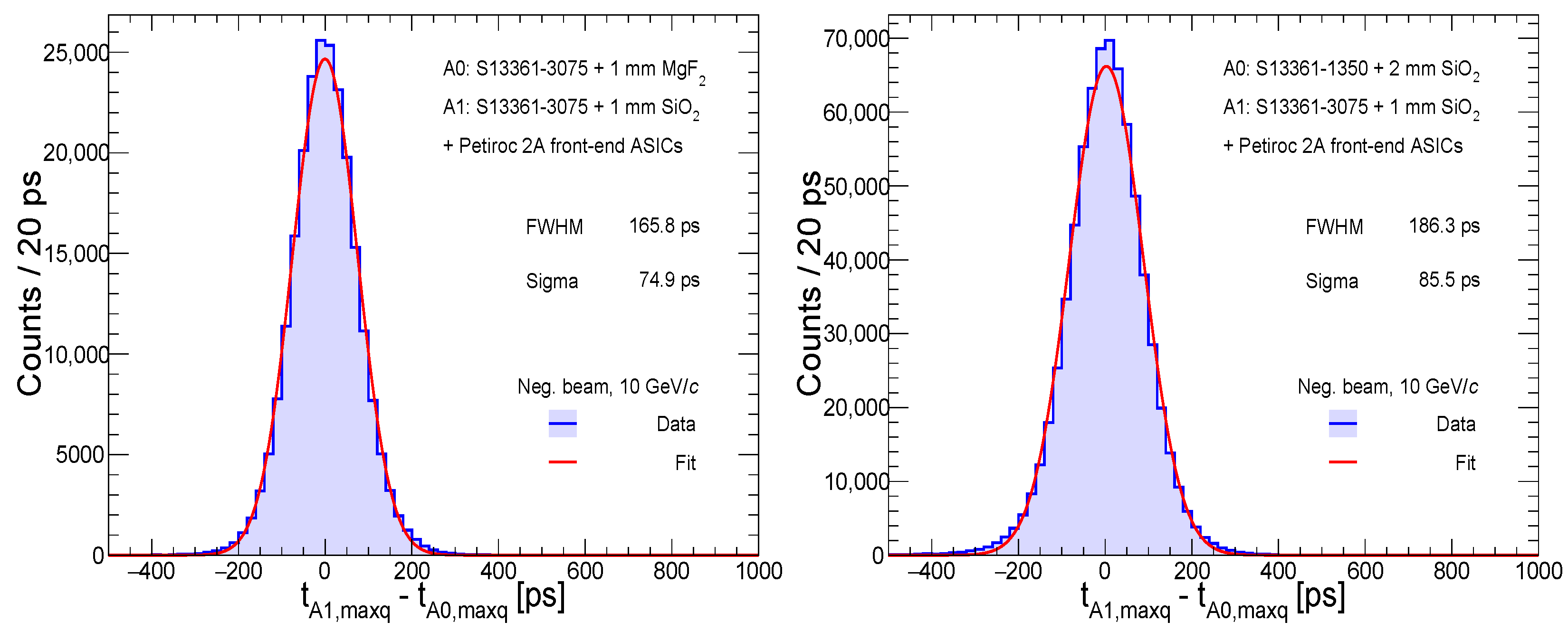
The left panel of Figure 14 shows the resulting distribution of the time difference between the SiPMs with maximum charge for the configuration with the S13361–3075 array coupled with a 1 mm thick SiO2 window (A1) and the S13361–3075 array coupled with a 1 mm thick MgF2 window (A0). The right panel of the same figure shows the corresponding distribution with the S13361–1350 array coupled with a 2 mm thick SiO2 window used as A0. The Gaussian fit to the distributions yields a resolution on the time difference σ Δ t , maxq of about 74.9 ps and 85.5 ps, respectively.
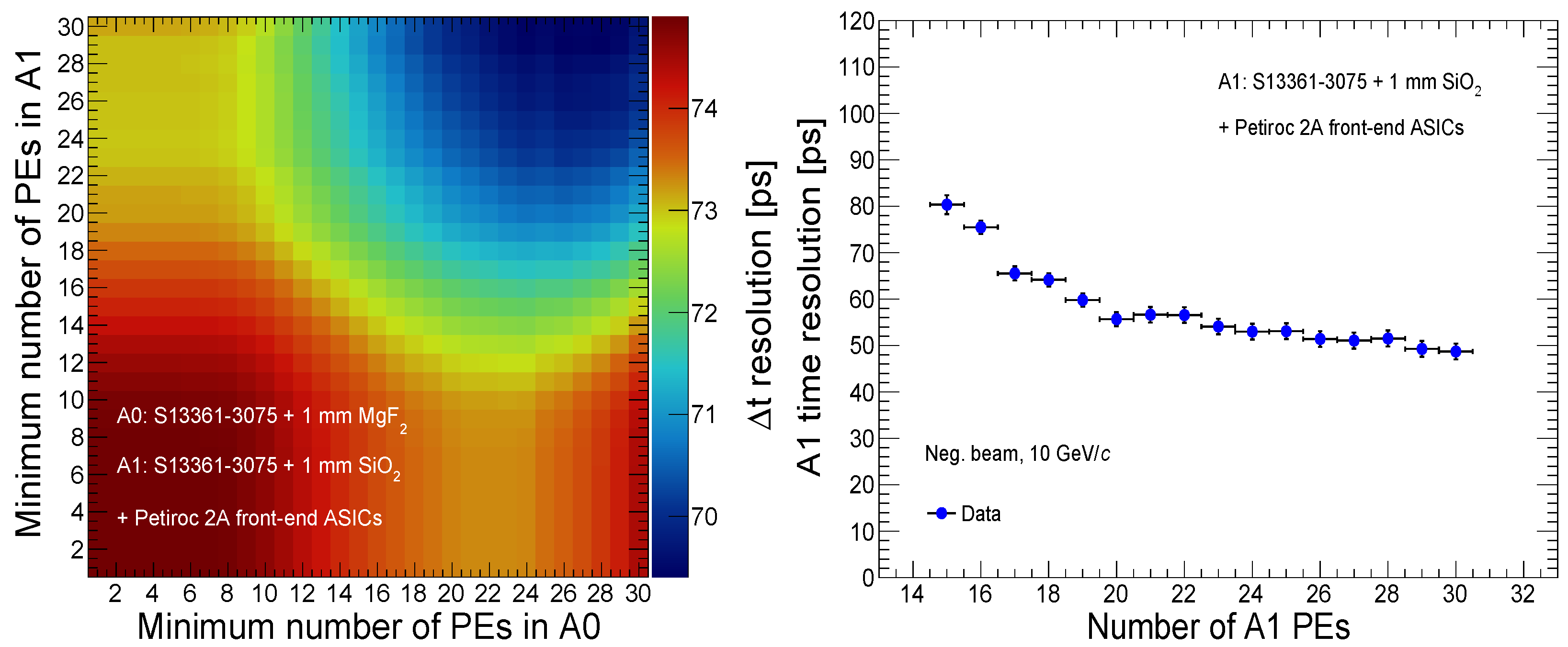
From the left panel of Figure 15, which shows the measured resolution of the time difference as a function of the minimum number of photoelectrons required in both A0 and A1 for the same configuration as the left panel of Figure 14, it can be observed that the contribution of the two S13361–3075 arrays with 1 mm SiO2 and MgF2 is almost identical. Since the measurements by the two arrays are independent, the observed 74.9 ps resolution on the time difference is, as a first approximation, the result of the sum in quadrature of two equal contributions. Therefore, this corresponds to a single-array time resolution σ t , maxq of approximately σ t , maxq = σ Δ t , maxq / 2 = 74.9 / 2 53.0 ps overall for both the S13361–3075 arrays read out with the Petiroc boards. Subtracting this contribution in quadrature from the σ Δ t , maxq of the distribution in the right panel of Figure 14, it is possible to extrapolate a σ t , maxq 67.1 ps for the S13361–1350 array with a 2 mm thick SiO2 window.
The left panel of Figure 15 also shows that, requiring more than 30 PEs in both the S13361–3075 arrays, a σ Δ t , maxq 70 ps is achieved, corresponding to a σ t , maxq ( N PE > 30 ) 49.5 ps for each of the S13361–3075 arrays. By scanning the σ Δ t , maxq values obtained at a fixed N PE in A0 (A1) while requiring N PE > 30 in A1 (A0), and then swapping the roles of A0 and A1, we found discrepancies in σ Δ t , maxq below 2.0 ps. We therefore assigned a systematic uncertainty of 2.0 / 2 1.4 ps to the extrapolated single array σ t , maxq ( N PE > 30 ) .
The right panel of Figure 15 shows the extrapolated σ t , maxq as a function of the number of PEs for the S13361–3075 array coupled with a 1 mm thick SiO2 window. We obtained the reported values by first extracting the σ Δ t , maxq relative to the S13361–3075 array coupled with a 1 mm thick window made of MgF2, by scanning over the number of PEs in that array and requiring more than 30 PEs in the reference array. We finally subtracted in quadrature the reference σ t , maxq ( N PE > 30 ) from all of the measured points to get the single-array resolution at a given number of PEs. We observed an overall improvement of σ t , maxq from 80 ps to 49 ps with the number of PEs increasing from 14 to 30.
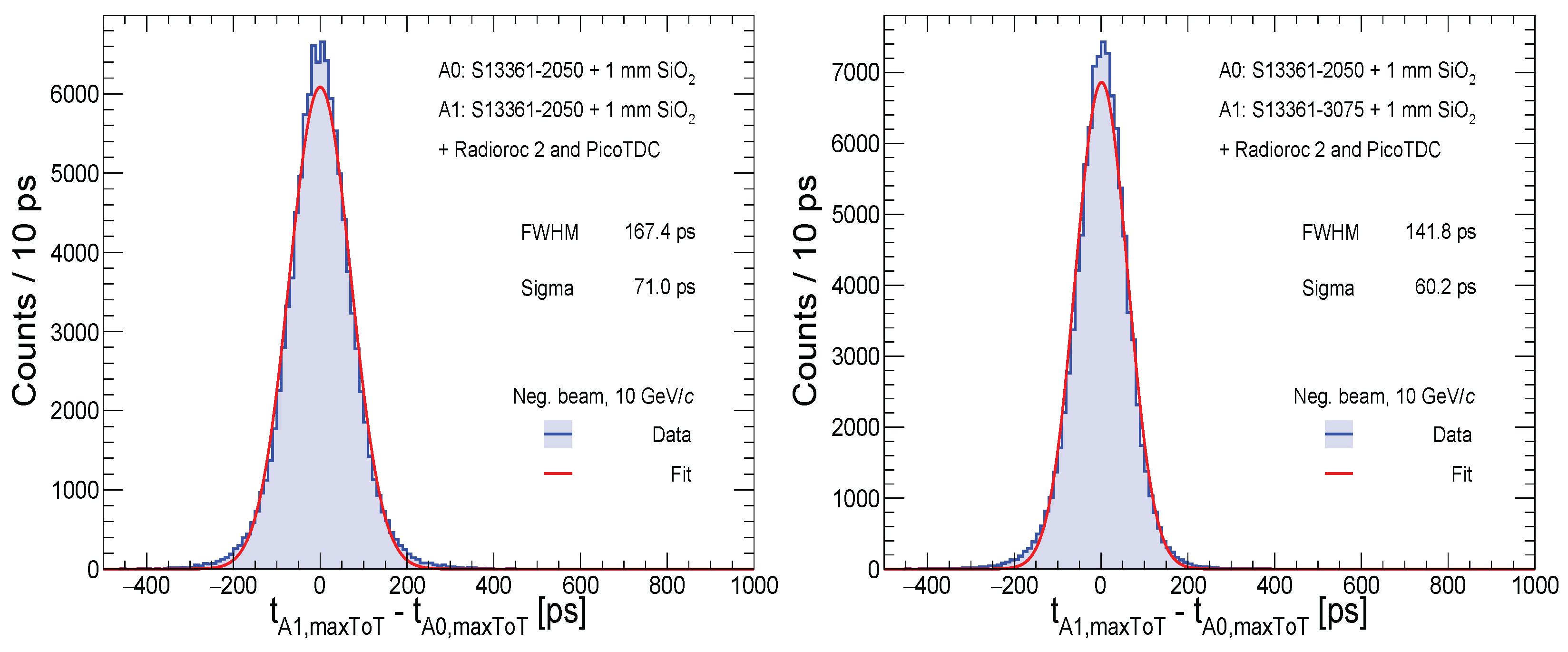
In order to highlight the impact of the front end on the time resolution, Figure 16 shows examples of the measured distributions of the time difference between the SiPMs with maximum ToT in the clusters for runs taken with the RadioPico boards. The left panel refers to the configuration with S13361–2050 arrays coupled with 1 mm thick SiO2 windows used as both A0 and A1. The right panel of the same figure shows the corresponding distribution with the S13361–3075 array coupled with a 1 mm thick SiO2 window used as A0.
In both cases, the expected resolution on the time difference would be intermediate relative to the configurations in Figure 14 if they were read out using the Petiroc boards. However, the Gaussian fit to the distributions yields a resolution on the time difference σ Δ t , maxToT of about 71.0 ps and 60.2 ps, respectively. Assuming equal contribution from the two S13361–2050 arrays, the measured 71.0 ps corresponds to an overall single-array time resolution σ t , maxToT 50.2 ps. Subtracting this value in quadrature from the σ Δ t , maxToT of the right panel of Figure 16, we extrapolated a σ t , maxToT 33.2 ps for the S13361–3075 array coupled with a 1 mm thick SiO2 window. Compared to the corresponding σ t , maxq 53.0 ps measured with the Petiroc boards, this result highlights the significantly better timing performance of the RadioPico boards and represents the best resolution measured in this study.

3.4.2. Analysis Using the Cluster Mean Time

The presence of multiple fired channels in the same cluster improves the achievable time resolution by averaging the respective timestamps. The effect is expected to be particularly relevant for windows thicker than the size of the considered SiPMs, as shown in Figure 2. In addition, the gain in time resolution also depends on the track impact region in the SiPMs of the array, as shown in Figure 11.
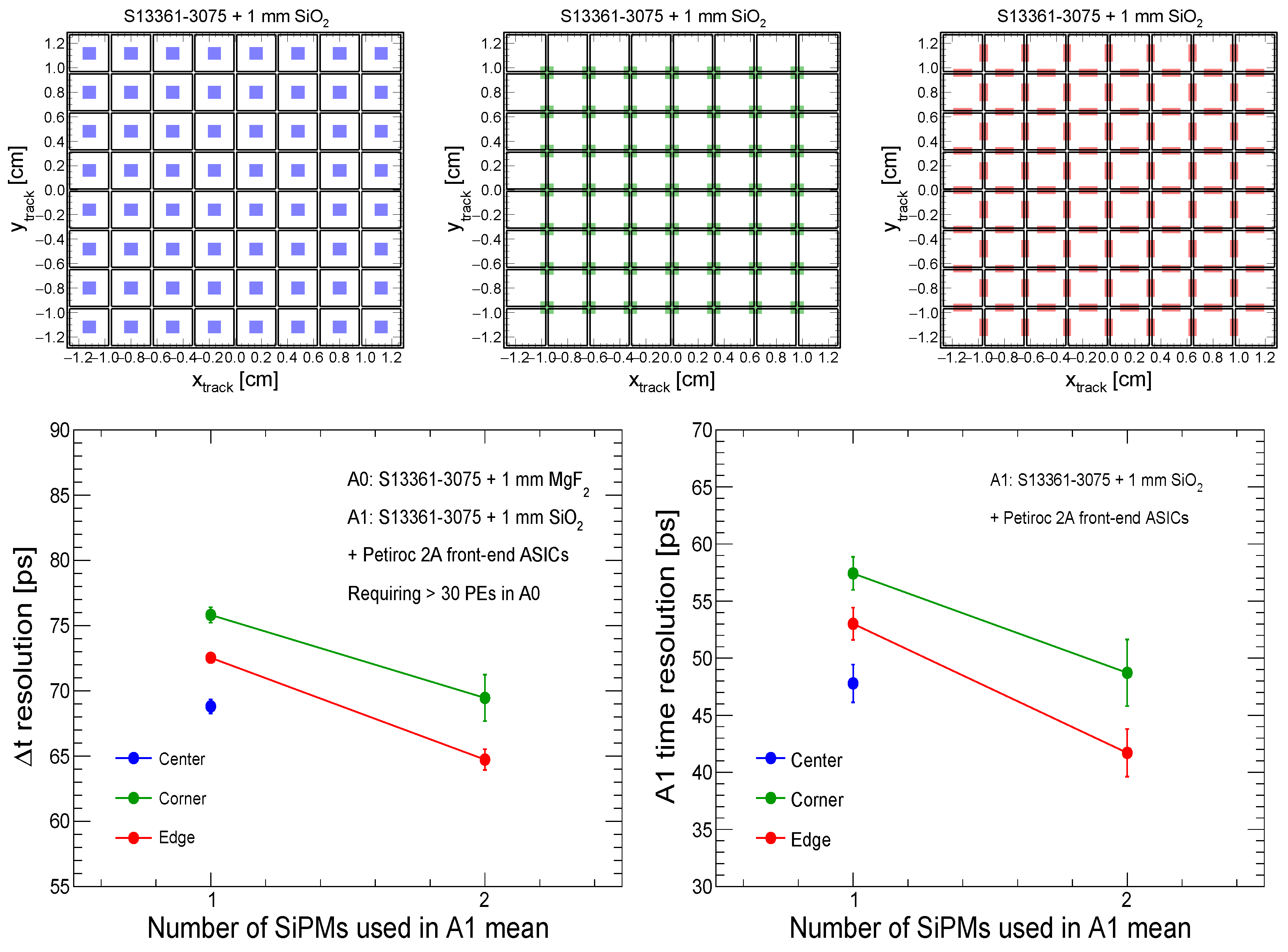
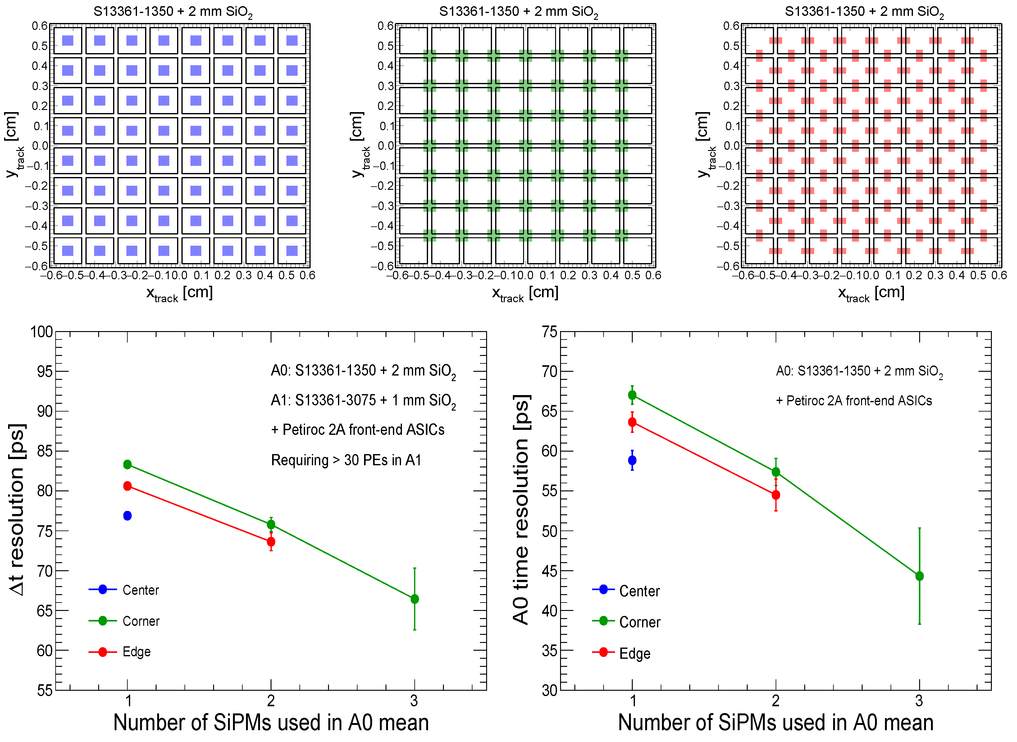
We investigated the spatial dependence of the time resolution for clusters of up to three fired channels. In order to address the possibility of achieving an improvement of the resolution as 1 / N SiPM for N SiPM fired channels with a sufficient number of PEs, we focused on runs taken with the Petiroc boards. We studied the clusters in the S13361–3075 array coupled with a 1 mm thick SiO2 window and the S13361–1350 array coupled with a 2 mm thick SiO2 window, considering the three regions illustrated in the top panels of Figure 17 and Figure 18, respectively. These correspond to the central regions of the SiPMs, the corners shared by four adjacent SiPMs, and the edges shared by two adjacent SiPMs.
We considered runs taken with one of these arrays and the S13361–3075 array coupled with a 1 mm thick window made either of MgF2 or of SiO2 used as a reference. We selected events requiring the charged track to cross the region of interest in the array under study and to release a maximum number of PEs larger than 30 in the reference array. We subsequently analyzed the clusters and calculated the mean time for the N highest-charge SiPMs up to N = 3 , requiring more than 16 PEs for the SiPMs of the S13361–3075 array and more than 9 PEs for the SiPMs of the S13361–1350 array to enter the calculation of the mean. Finally, we evaluated the difference relative to the time of the SiPM with maximum charge in the reference array, and we built the corresponding distributions.
The bottom-left panels of Figure 17 and Figure 18 show the results obtained from the Gaussian fits to the corresponding distributions as a function of the number of SiPMs used in the mean for the three considered regions. Only points with enough available statistics are shown. The bottom-right panels of the same figures show the corresponding resolutions at the single-array level, by subtracting in quadrature the contribution of the reference array, ( 49.5 ± 1.4 ) ps, calculated as discussed above. As expected, when considering only the SiPM with maximum charge, the best resolution is achieved for tracks incident at the SiPM center, while it degrades for incidence at the edges and is worst at the corners. Including more SiPMs in the mean, the resolution at the edges and at the corners improves. The improvement is particularly visible for the S13361–1350 array with 2 mm SiO2, due to the more uniform charge-sharing among the SiPMs. In particular, the observed resolution scaling at the corners of this array approaches the ideal 1 / N SiPM dependence, improving from about 67 ps to about 44 ps. Similar considerations also apply to the edges. For the S13361–3075 array, we observed a softer dependence, attributed to the unbalanced sharing of the charge in combination with the limited 1 mm thickness of the window.

3.5. Comparison with a Bare SiPM Array

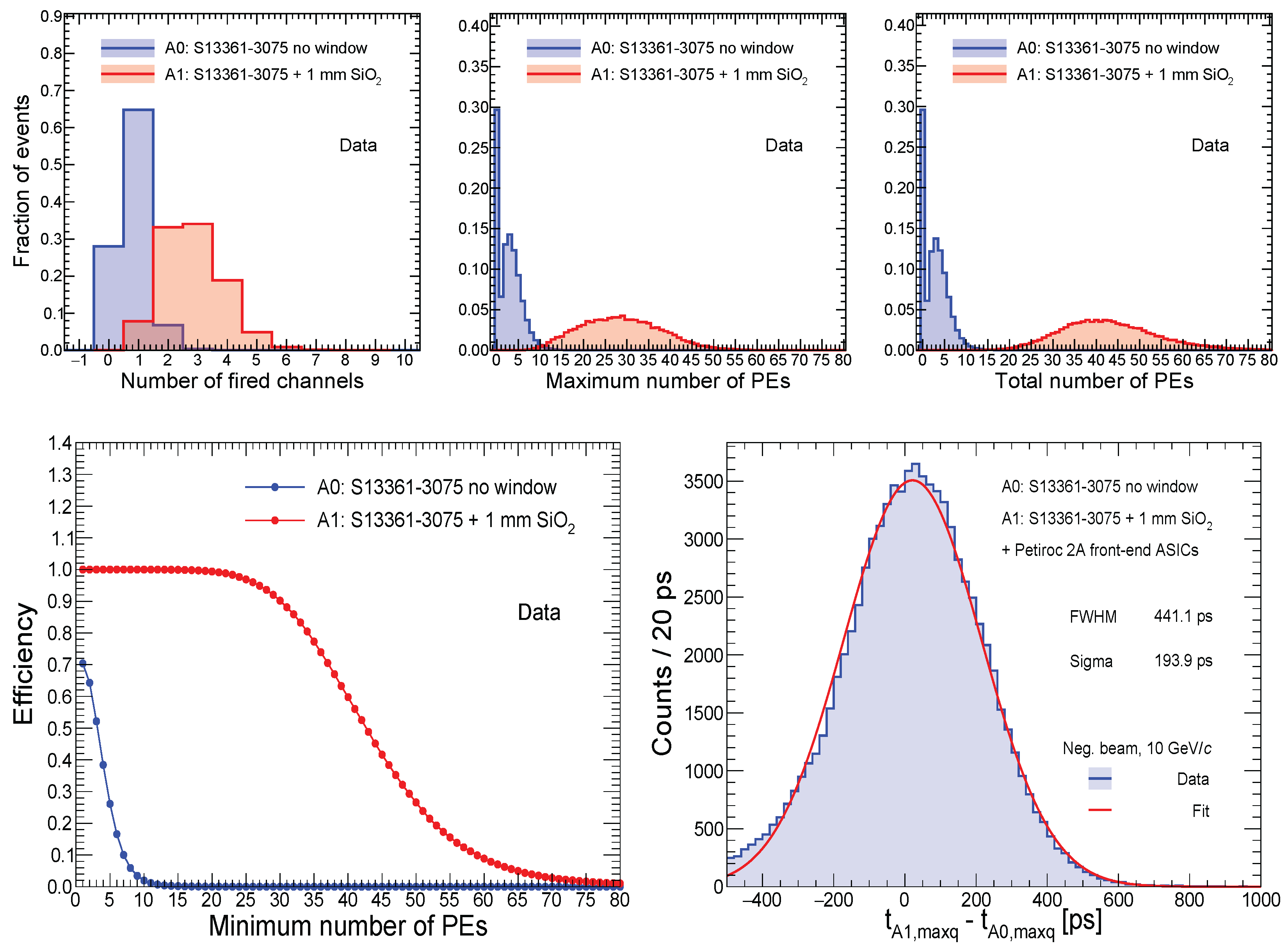
The impact of the Cherenkov signal from the tested windows, as well as the results discussed above, can be clearly shown by comparing them with the case of an array of bare SiPMs. Figure 19 shows the distributions of the number of fired channels and the charge in the clusters, the measured efficiency, and the distribution of the time difference between the SiPMs with maximum charge for the configuration with S13361–3075 arrays, one coupled with a 1 mm thick SiO2 window and one with no external window, used as A1 and A0, respectively. Despite the lower threshold set for the A0 array, as discussed in Section 2.5.6, there are about 30% of the events in which the array is not responding at all, and about 65% where a single channel is fired, resulting in a limited charged-particle detection efficiency. Nevertheless, a maximum charge corresponding to up to 10 PEs is still observed for the events where the array is responding. As confirmed by the comprehensive Geant4 simulation of this configuration, these PEs result from both the Cherenkov emission in the 100 μ m thick built-in epoxy resin layer and the direct ionization loss in the silicon-depleted region, as well as Cherenkov photons produced in the upstream Ar volume and the correlated cross-talk of the SiPMs. The resolution of the time difference between the SiPMs with maximum charge in A0 and A1 is σ Δ t , maxq 193.9 ps. By subtracting in quadrature the extrapolated contribution of A1 (about 53.0 ps), we found a single-array time resolution σ t , maxq 186.5 ps for the array with no window. This result is significantly worse than those obtained for all configurations with a window, highlighting the substantial performance gains in terms of signal strength, efficiency, and time resolution achievable with the considered timing approach when a radiator window is included.

4. Discussion

On the basis of the excellent performance in terms of efficiency and time resolution demonstrated in the previous section, the following considerations can be made.
The optimization of the sensor and radiator parameters (SiPM size and pitch, SPAD pitch, and window thickness) is crucial to achieve the best time resolution. Simulations and measurement results show that the optimal radiator configuration, in terms of both spectral response and the detected photon yield, is a SiO2 window coupled with SiPMs using silicone resin, which provides the best optical coupling and NUV transmittance.
Independent of the SiPM size, a window thickness of about 1 mm is sufficient to achieve full charged-particle detection efficiency operating with thresholds of up to tens of PEs, thereby suppressing background from the DCR even in high-radiation environments.
While smaller SiPMs are typically expected to provide better single-photon timing due to their lower terminal capacitance [7], in the present multi-photon regime larger SiPMs collect substantially more photoelectrons in the same pixel. Larger SiPMs yield the best time resolution when exploiting the channel with maximum charge in the clusters.
At the same time, smaller SiPMs result in a more uniform charge-sharing across channels, which enables timing improvements by averaging the detection times of multiple SiPMs in the cluster. The observed time resolution exhibits the expected improvement with the number of fired SiPM channels, scaling approximately as 1 / N SiPM within the experimental uncertainties. For larger SiPMs, instead, except for tracks incident near SiPM boundaries, neighboring channels typically collect only a limited charge. Consequently, including their timing information could even worsen the time resolution. A more uniform charge-sharing is achieved by increasing the ratio between the window thickness and the SiPM pitch in the array. The performance is also influenced by the larger SPAD pitch, which results in a larger fill factor and, consequently, a higher PDE. This effect can be clearly observed by comparing the results achieved with the S13361–3075 and S13361–1350 arrays.
The comparison between the results achieved with Petiroc and RadioPico boards shows that, in order to fully exploit the intrinsic timing potential of the proposed approach, the use of front-end electronics with very low jitter is mandatory. Using the RadioPico boards, we achieved the best time resolution reported in this study—about 33.2 ps—for the S13361–3075 arrays coupled with a 1 mm thick SiO2 window. This result might be further improved with larger calibration statistics, which would enable a more precise offset equalization over the full array and the inclusion of the dependence on the track impact position in the considered lookup-table procedure.
The ultimate performance of the tested setup is affected by signal-integrity limitations of the test-beam cabling scheme, including the HLCD–20 cables and the feed-through board, which degrade the analog signal quality with respect to an ideal direct coupling, especially at low photoelectron yields.
Further improvements in both efficiency and timing are expected with dedicated developments, such as custom ARCs optimized for the wavelength-dependent Cherenkov spectrum, the polarization of Cherenkov photons, and the SiPM spectral response, designed to maximize photon collection over the relevant charged track and photon incidence-angle distributions by reducing reflections and increasing the effective SiPM PDE.
As a final consideration, it is worth highlighting that preserving the overall performance while integrating TOF devices into a full HEP experiment requires the implementation of appropriate design optimizations.

5. Conclusions

We have shown that time resolutions of a few tens of ps can be readily achieved with full charged-particle detection efficiency by detecting the Cherenkov photons emitted by charged particles traversing a thin slab of fused silica coupled to a SiPM array. Devices based on this approach represent a step forward in particle identification systems for future HEP experiments planning to extend the identification of charged particles to higher momenta. As collider luminosities increase, the developed timing sensors will also be compulsory for pile-up suppression and 4D tracking.

Author Contributions

Conceptualization, M.N.M., G.D.R., F.L., E.N. and N.N.; methodology, M.N.M., L.C., G.D.R., F.L., E.N., N.N. and R.P.; software, L.C., G.D.R., M.G., A.L., L.L., N.N., G.P. and R.P.; validation, M.G., A.L., L.L., N.N., G.P. and R.P.; formal analysis, M.G., A.L., L.L., N.N., G.P. and R.P.; investigation, M.N.M., M.G., A.L., R.L., L.L., N.N., G.P. and R.P.; resources, A.D.M., L.C., M.N.M., G.D.R., M.G., F.L., A.L., L.L., N.N., G.P. and R.P.; data curation, M.N.M., M.G., A.L., L.L., N.N., G.P. and R.P.; writing—original draft preparation, M.N.M., E.N., N.N. and R.P.; writing—review and editing, M.N.M., E.N. and N.N.; visualization, M.N.M., N.N. and R.P.; supervision, M.N.M. and R.P.; project administration, A.D.M., M.N.M. and G.V.; funding acquisition, M.N.M. All authors have read and agreed to the published version of the manuscript.

Funding

This research received no external funding.

Data Availability Statement

The datasets generated and/or analyzed during the present study are available from the corresponding author upon reasonable request.

Acknowledgments

The authors would like to thank the INFN Bari staff for their contribution to the procurement and the construction of the prototype. In particular, we thank D. Dell’Olio, M. Franco, N. Lacalamita, F. Maiorano, M. Mongelli, C. Pastore, and R. Triggiani for their technical support. The authors would like to thank Weeroc for contributing to the development of the Radioroc 2/picoTDC board and providing support for the operation of Radioroc 2. We also thank the CERN beam team for providing the facilities and logistical support for the test. This work was carried out in the context of the DRD4 Collaboration based at CERN.

Conflicts of Interest

The authors declare no conflicts of interest.

Abbreviations

The following abbreviations are used in this manuscript:
ADCAnalog-to-Digital Converter
DAQData Acquisition
FEBFront-End Board
FFFill Factor
IFIntegration Factor
LSBLeast Significant Bit
LUTLookup Table
MPPCMulti-Pixel Photon Counter
NaFSodium Fluoride
PEPhotoelectron
PDEPhotom Detection Efficiency
PIDParticle Identification
RICHRing-Imaging Cherenkov
SPADSingle-Photon Avalanche Diode
SiPMSilicon Photomultiplier
TOFTime of Flight
ToATime of Arrival
ToTTime over Threshold

Appendix A. Modeling the SiPM Reflectance

On the basis of hypotheses about the sources of specular and diffuse reflection in the tested arrays, we formulated a simple model for the specular and diffuse reflectance, R spec and R diff . As a first approximation, specular reflections are assumed within the SiPM active regions, while diffuse reflections are assumed in the dead regions of a SiPM or between adjacent SiPMs in the array. Let g denote the gas surrounding the array, w the window, and r the protective resin. Let FF be the fill factor, i.e., the fraction of the active area of a single SiPM, and IF the integration factor, i.e., the fraction of the array area covered by the SiPMs. Our model is based on the following assumptions:
  • Only specular reflection R x y with x , y = g , w , r occurs at the smooth interfaces between gas and resin, gas and window, and window and resin.
  • Only specular reflection R r ARC Si occurs at the resin–ARC–passivation–silicon interfaces within the active area, corresponding to a fraction IF · FF of the array area.
  • Only diffuse reflection R diff , 1 occurs in the dead area within any SiPM, corresponding to a fraction IF ( 1 FF ) of the array area.
  • Only diffuse reflection R diff , 2 occurs in the dead area between adjacent SiPMs, corresponding to a fraction 1 IF of the array area.
The following expressions are derived for the reflectances R spec and R diff for the wavelength region where absorption effects in the window or protective resin are negligible:
R spec = R g w + ( 1 R g w ) R w r + ( 1 R g w ) ( 1 R w r )   · IF · FF · R r ARC Si · ( 1 R r w ) ( 1 R w g ) ,
R diff = ( 1 R g w ) ( 1 R w r ) · [ ( 1 IF ) · R diff , 2   + IF · ( 1 FF ) · R diff , 1 ] · ( 1 R diff , r w g ) .
The terms R x y are obtained from Fresnel equations [43] using the known refractive indices of the media x and y, the photon incidence angle, and the transmission angles in the considered media determined via Snell’s law. For arrays without resin, the corresponding equations are obtained by setting w = g and R g g = 0 .
The term R diff , r w g represents the mean reflectance for photons that undergo a diffuse reflection in the dead area within a SiPM or between adjacent SiPMs, possibly followed by specular reflections at the resin, window, and gas interfaces. For the studies carried out using this model, we evaluated it with dedicated Monte Carlo simulations assuming, as a first approximation, an isotropic random reflection angle in the dead regions within the array.
The terms R r ARC Si , R diff , 1 , and R diff , 2 are not known a priori, due to the limited information on the SiPM ARC and the microstructures in the dead regions. However, R r ARC Si can be easily inferred from the measured specular reflectance by inverting Equation (A1):
R r ARC Si = R spec R g w ( 1 R g w ) R w r ( 1 R g w ) ( 1 R w r ) · IF · FF · ( 1 R r w ) ( 1 R w g )
The expression for arrays without resin is obtained by setting w = g , giving R g g = 0 .

References

  1. Nappi, E.; Seguinot, J. Ring imaging Cherenkov detectors: The state of the art and perspectives. Riv. Nuovo Cim. 2005, 28, 1–130. [Google Scholar] [CrossRef]
  2. Credo, T.; Frisch, H.; Sanders, H.; Schroll, R.; Tang, F. Picosecond time-of-flight measurement for colliders using Cherenkov light. In Proceedings of the IEEE Symposium Conference Record Nuclear Science 2004; IEEE: Piscataway, NJ, USA, 2004; Volume 1, pp. 586–590. [Google Scholar] [CrossRef]
  3. Inami, K.; Kishimoto, N.; Enari, Y.; Nagamine, M.; Ohshima, T. A 5-ps TOF-counter with an MCP-PMT. Nucl. Instrum. Meth. A 2006, 560, 303–308. [Google Scholar] [CrossRef]
  4. Krizan, P. Proximity focusing RICH with TOF capabilities. J. Phys. Conf. Ser. 2008, 110, 092015. [Google Scholar] [CrossRef]
  5. Va’vra, J.; Leith, D.W.G.S.; Ratcliff, B.; Ramberg, E.; Albrow, M.; Ronzhin, A.; Ertley, C.; Natoli, T.; May, E.; Byrum, K. Beam Test of a Time-of-Flight Detector Prototype. Nucl. Instrum. Meth. A 2009, 606, 404–410. [Google Scholar] [CrossRef][Green Version]
  6. Albrow, M.G.; Kim, H.; Los, S.; Mazzillo, M.; Ramberg, E.; Ronzhin, A.; Samoylenko, V.; Wenzel, H.; Zatserklyaniy, A. Quartz Cherenkov Counters for Fast Timing: QUARTIC. J. Instrum. 2012, 7, P10027. [Google Scholar] [CrossRef]
  7. Gundacker, S.; Heering, A. The silicon-photomultiplier: Fundamentals and applications of a modern solid-state photon detector. Phys. Med. Biol. 2020, 65, 17TR01. [Google Scholar] [CrossRef]
  8. Carnesecchi, F.; Sabiu, B.; Strazzi, S.; Vignola, G.; Agrawal, N.; Alici, A.; Antonioli, P.; Arcelli, S.; Bellini, F.; Cavazza, D.; et al. Measurements of the Cherenkov effect in direct detection of charged particles with SiPMs. Eur. Phys. J. Plus 2023, 138, 788. [Google Scholar] [CrossRef]
  9. Mazziotta, M.N.; Di Mauro, A.; Giliberti, M.; Liguori, A.; Lorusso, L.; Nappi, E.; Nicassio, N.; Panzarini, G.; Pillera, R.; Volpe, G. Efficient and precise Cherenkov-based charged particle timing using SiPMs. Nucl. Instrum. Meth. A 2026, 171648. [Google Scholar] [CrossRef]
  10. Vinke, R.; Löhner, H.; Schaart, D.; van Dam, H.; Seifert, S.; Beekman, F.; Dendooven, P. Optimizing the timing resolution of SiPM sensors for use in TOF-PET detectors. Nucl. Instrum. Meth. A 2009, 610, 188–191. [Google Scholar] [CrossRef]
  11. Riegler, W.; Windischhofer, P. Time resolution and efficiency of SPADs and SiPMs for photons and charged particles. Nucl. Instrum. Meth. A 2021, 1003, 165265. [Google Scholar] [CrossRef]
  12. Malitson, I.H. Interspecimen Comparison of the Refractive Index of Fused Silica. J. Opt. Soc. Am. 1965, 55, 1205. [Google Scholar] [CrossRef]
  13. Navas, S.; Amsler, C.; Gutsche, T.; Hanhart, C.; Hernández-Rey, J.; Lourenço, C.; Masoni, A.; Mikhasenko, M.; Mitchell, R.; Patrignani, C.; et al. Review of particle physics. Phys. Rev. D 2024, 110, 030001. [Google Scholar] [CrossRef]
  14. Hamamatsu Photonics K.K. Solid State Division, Hamamatsu City, Japan—S13360 series. Available online: https://www.hamamatsu.com/eu/en/product/optical-sensors/mppc/mppc_mppc-array/S13360-3075CS.html (accessed on 21 February 2026).
  15. Wang, W.; Cao, G.; Xie, Z.; Cao, J.; Qi, M.; Wen, L. Reflectance of silicon photomultipliers in linear alkylbenzene. Nucl. Instrum. Meth. A 2020, 973, 164171. [Google Scholar] [CrossRef]
  16. Hamamatsu Photonics K.K. Solid State Division, Hamamatsu City, Japan—S13361–2050AE-08. Available online: https://www.hamamatsu.com/eu/en/product/optical-sensors/mppc/mppc_mppc-array/S13361-2050AE-08.html (accessed on 21 February 2026).
  17. Agilent Technologies, Inc. Santa Clara, CA, USA—Diffuse Reflectance Accessory—External DRA 900/1800/2500. Available online: https://community.agilent.com/cfs-file/__key/docpreview-s/00-00-00-97-98/Cary-Help-DRA-1800.pdf (accessed on 21 February 2026).
  18. Agilent Technologies, Inc. Santa Clara, CA, USA—Cary 100/300/4000/5000/6000i/7000 Spectrophotometers User’s Guide. Available online: https://www.agilent.com/en/product/molecular-spectroscopy/uv-vis-uv-vis-nir-spectroscopy/uv-vis-uv-vis-nir-systems/cary-4000-uv-vis (accessed on 21 February 2026).
  19. van Dijk, M.; Hayat, A.; Banerjee, D.; Bernhard, J.; Gokturk, B.; Nevay, L.; Petersen, J.; Schwinzerl, M. Particle production and identification for the T10 secondary beamline of the CERN East Area. Nucl. Instrum. Meth. B 2025, 569, 165907. [Google Scholar] [CrossRef]
  20. Optical Cement EJ-500. Available online: https://eljentechnology.com/products/accessories/ej-500 (accessed on 17 April 2026).
  21. Hamamatsu Photonics K.K. Solid State Division, Hamamatsu City, Japan—S13552. Available online: https://www.hamamatsu.com/eu/en/product/optical-sensors/mppc/mppc_mppc-array/S13552.html (accessed on 21 February 2026).
  22. Mazziotta, M.N.; Altomare, C.; Bissaldi, E.; De Gaetano, S.; De Robertis, G.; Dipinto, P.; Venere, D.L.; Franco, M.; Fusco, P.; Gargano, F.; et al. A light tracker based on scintillating fibers with SiPM readout. Nucl. Instrum. Meth. A 2022, 1039, 167040. [Google Scholar] [CrossRef]
  23. Pillera, R.; Altomare, C.; De Robertis, G.; Di Venere, L.; Gargano, F.; Giliberti, M.; Loparco, F.; Loporchio, S.; Lorusso, L.; Panzarini, G.; et al. Characterization of a light fiber tracker prototype with SiPM array readout. In Proceedings of the 9th International Workshop on Advances in Sensors and Interfaces; IEEE: Piscataway, NJ, USA, 2023. [Google Scholar] [CrossRef]
  24. Cerasole, D.; De Palma, G.; De Robertis, G.; Di Venere, L.; Gargano, F.; Giliberti, M.; Licciulli, F.; Liguori, A.; Loizzo, P.; Loparco, F.; et al. Development of a light tracker based on thin scintillating fibers and Silicon Photomultipliers for space application. Nucl. Instrum. Meth. A 2026, 1082, 171064. [Google Scholar] [CrossRef]
  25. TEWA TT4-10KC3-T125-M5-500 NTC Thermistor. Available online: https://www.tme.eu/Document/6d2e1b5322209ea0890793c756dbc659/TT4-10KC3-T125-M5-500.pdf (accessed on 21 February 2026).
  26. Raspberry Pi Foundation. Raspberry Pi 3 Model B. Single-Board Computer. Available online: https://www.raspberrypi.com/products/raspberry-pi-3-model-b/ (accessed on 21 February 2026).
  27. ADS1115 16-Bit ADC—4 Channel with Programmable Gain Amplifier—STEMMA QT/Qwiic. Available online: https://www.adafruit.com/product/1085 (accessed on 21 February 2026).
  28. DS18B20 1-Wire Digital Thermometer. Available online: https://www.maximintegrated.com/en/products/sensors/DS18B20.html (accessed on 21 February 2026).
  29. Adafruit Sensirion SHT31-D-Temperature & Humidity Sensor. Available online: https://www.adafruit.com/product/2857 (accessed on 21 February 2026).
  30. Samtec LSHM-120-02.5-L-DV-A-N-K-TR Connector. Available online: https://www.samtec.com/products/lshm (accessed on 21 February 2026).
  31. Samtec ST4-40-1.00-L-D-P-TR Connector. Available online: https://www.samtec.com/products/st4-40-1.00-l-d-p-tr (accessed on 21 February 2026).
  32. Samtec SS4-40-3.00-L-D-K-TR Connector. Available online: https://www.samtec.com/products/ss4-40-3.00-l-d-k-tr (accessed on 21 February 2026).
  33. Samtec HLCD-20-06.00-TR-TR-1 Cable. Available online: https://www.samtec.com/products/hlcd (accessed on 21 February 2026).
  34. CAEN A7585D 1 Ch. 85 V/10 mA Digital Controlled SiPM Power Supply. Available online: https://www.caen.it/products/a7585/ (accessed on 21 February 2026).
  35. Petiroc 2A by Omega and Weeroc, France. Available online: https://www.weeroc.com/read_out_chips/petiroc-2a/ (accessed on 21 February 2026).
  36. Saleem, T.; Ahmad, S.; Cizel, J.B.; De La Taille, C.; Morenas, M.; Nadig, V.; Perez, F.; Schulz, V.; Gundacker, S.; Fleury, J. Study experimental time resolution limits of recent ASICs at Weeroc with different SiPMs and scintillators. J. Instrum. 2023, 18, P10005. [Google Scholar] [CrossRef]
  37. Altruda, S.; Christiansen, J.; Horstmann, M.; Perktold, L.; Porret, D.; Prinzie, J. PicoTDC: A flexible 64 channel TDC with picosecond resolution. J. Instrum. 2023, 18, P07012. [Google Scholar] [CrossRef]
  38. AMD Kintex-7 FPGA Module. Available online: https://www.enclustra.com/en/products/fpga-modules/mercury-kx2 (accessed on 21 February 2026).
  39. Robertis, G.D.; Fanizzi, G.; Loddo, F.; Manzari, V.; Rizzi, M. A MOdular System for Acquisition, Interface and Control (MOSAIC) of detectors and their related electronics for high energy physics experiment. EPJ Web Conf. 2018, 174, 07002. [Google Scholar] [CrossRef]
  40. Weeroc. Radioroc 2: Multi-Purpose SiPM Analogue Read-Out ASIC. 64-Channel SiPM Front-End ASIC with Dual-Gain Readout and Sub-50ps Timing. Available online: https://www.weeroc.com/read_out_chips/radioroc-2/ (accessed on 21 February 2026).
  41. CERN PicoTDC Team. PicoTDC ASIC Project Website. Official CERN project website for the PicoTDC ASIC. Available online: https://picotdc.web.cern.ch/ (accessed on 21 February 2026).
  42. Skyworks Solutions, Inc. SI5341-D-EVB: Si5341 Clock Generator Evaluation Board. Evaluation Board for the Si5341 Ultra-Low Jitter Clock Generator. Available online: https://www.skyworksinc.com/en/products/timing/evaluation-kits/clock/si5341-evaluation-kit (accessed on 21 February 2026).
  43. Steck, D.A. Classical and Modern Optics. Available online: https://atomoptics.uoregon.edu/~dsteck/teaching/optics/ (accessed on 21 February 2026).
  44. de Marcos, L.V.R.; Larruquert, J.I.; Méndez, J.A.; Aznárez, J.A. Self-consistent optical constants of MgF2, LaF3, and CeF3 films. Opt. Mater. Express 2017, 7, 989–1006. [Google Scholar] [CrossRef]
  45. Ozaki, S.; Adachi, S. Optical Constants of Cubic ZnS. J. Appl. Phys. 1993, 32, 5008. [Google Scholar] [CrossRef]
  46. Bright, T.J.; Watjen, J.I.; Zhang, Z.M.; Muratore, C.; Voevodin, A.A. Optical properties of HfO2 thin films deposited by magnetron sputtering: From the visible to the far-infrared. Thin Solid Films. 2012, 520, 6793–6802. [Google Scholar] [CrossRef]
  47. Jolivet, A.; Labbé, C.; Frilay, C.; Debieu, O.; Marie, P.; Horcholle, B.; Lemarié, F.; Portier, X.; Grygiel, C.; Duprey, S.; et al. Structural, optical, and electrical properties of TiO2 thin films deposited by ALD: Impact of the substrate, the deposited thickness and the deposition temperature. Appl. Surf. Sci. 2023, 608, 155214. [Google Scholar] [CrossRef]
  48. Agostinelli, S.; Allison, J.; Amako, K.; Apostolakis, J.; Araujo, H.; Arce, P.; Asai, M.; Axen, D.; Banerjee, S.; Barrand, G.; et al. GEANT4—A Simulation Toolkit. Nucl. Instrum. Meth. A 2003, 506, 250–303. [Google Scholar] [CrossRef]
  49. Allison, J.; Amako, K.; Apostolakis, J.; Araujo, H.; Dubois, P.A.; Asai, M.; Barrand, G.; Capra, R.; Chauvie, S.; Chytracek, R.; et al. Geant4 developments and applications. IEEE Trans. Nucl. Sci. 2006, 53, 270–278. [Google Scholar] [CrossRef]
  50. Allison, J.; Amako, K.; Apostolakis, J.; Arce, P.; Asai, M.; Aso, T.; Bagli, E.; Bagulya, A.; Banerjee, S.; Barrand, G.; et al. Recent developments in Geant4. Nucl. Instrum. Meth. A 2016, 835, 186–225. [Google Scholar] [CrossRef]
Figure 1. Three-dimensional model of the radiator–sensor coupling. The incident particle track is shown passing through the radiator. The Cherenkov radiation is projected onto the SiPM array layer, highlighting the spatial correlation between the particle trajectory and the fired pixels. The red–orange area corresponds to the core of the emission, assuming negligible reflections at the radiator boundaries.
Instruments 10 00028 g001
Figure 2. (Top left): Expected time resolution as a function of the SiO2 radiator thickness. The colored curves represent the individual contributions to the total time resolution. (Top right): Average number of fired pixels as a function of the radiator thickness. (Bottom left): Average number of photoelectrons collected in the three pixels with the highest hit probability, shown as a function of the radiator thickness. (Bottom right): Total time resolution as a function of the radiator thickness, computed using the timestamps from the three highest-charge channels. Three SiPM configurations were investigated: 3 mm active area with a 75 μ m SPAD size, 2 mm active area with a 50 μ m SPAD size, and 1.3 mm active area with a 50 μ m SPAD size.
Instruments 10 00028 g002
Figure 3. Schematic view of the detector stack, including the environmental gas, the window, and the SiPMs. The SiPM structure includes the protective resin, the ARC, the passivation layer, and silicon.
Instruments 10 00028 g003
Figure 4. (Top): Schematic view of the beam test setup. (Bottom): Photographs of the cylindrical vessel housing the arrays A0 and A1, and their connection to the front-end boards.
Instruments 10 00028 g004
Figure 5. ToT measured from the digital output signal of the Radioroc 2, which is given as input to the picoTDC, versus shaper charge measured from the analog probe output of the shaper (left panel). The measurements were performed with an oscilloscope while illuminating a single SiPM with a laser. The one-dimensional projections of the ToT and charge are displayed (right panel).
Instruments 10 00028 g005
Figure 6. Measured total reflectance (top left), diffuse reflectance (top right), and specular reflectance (bottom left) for Hamamatsu S13361 series 8 × 8 arrays of 3 × 3 mm2 SiPMs, spanning different SPAD pitches, protective resins, and window materials (see Table 1). The (bottom right) panel compares total reflectance for arrays with 3 × 3 mm2 and 2 × 2 mm2 active area that share the same 50 µm SPAD pitch and the same protective layer made of epoxy resin.
Instruments 10 00028 g006
Figure 7. Reflectance at the SiPM resin–ARC–passivation–silicon interfaces R r ARC Si extrapolated from the measured specular reflectance using Equation (A3) (Appendix A) for the tested arrays as a function of wavelength.
Instruments 10 00028 g007
Figure 8. Expected reflectance as a function of wavelength for custom ARCs made of 81 nm CeF3 + 31 nm ZnS (left) and 35 nm HfO2 + 23 nm TiO2 (right), optimized for Cherenkov photons emitted by normally incident charged particles at the Cherenkov angle saturation in a SiO2 window ( θ C 47 ). A 100 μ m thick silicone resin protective layer and a 10 nm thick SiO2 passivation layer on top of silicon are assumed. The different curves correspond to various photon emission angles to illustrate the reflectance for photons emitted in the regime between the Cherenkov threshold and saturation.
Instruments 10 00028 g008
Figure 9. Measured (top panels) and simulated (bottom panels) distributions of the number of fired SiPMs (left), the maximum charge in a single SiPM (middle), and the total number of photoelectrons (right) in the clusters for runs taken with the negatively charged beam at 10 GeV/c using Petiroc boards. The plots refer to the configuration with two S13361–3075 arrays coupled with a 1 mm thick SiO2 window (A1) and a 1 mm thick MgF2 window (A0).
Instruments 10 00028 g009
Figure 10. Measured (top) and simulated (bottom) distributions of the number of fired channels (left), the maximum charge in a single SiPM (middle), and the total number of photoelectrons (right) in the clusters for runs taken with the negatively charged beam at 10 GeV/c using Petiroc boards. The plots refer to the configuration with the S13361–3075 array coupled with a 1 mm thick SiO2 window (A1) and the S13361–1350 array coupled with a 2 mm thick SiO2 window (A0).
Instruments 10 00028 g010
Figure 11. Measured mean number of fired channels (left), mean maximum charge in a single SiPM (middle), and mean total number of photoelectrons (right) in the clusters as a function of the track impact point ( x track , y track ) on the SiPM arrays for runs taken with the negatively charged beam at 10 GeV/c using Petiroc boards. The plots refer to the configurations with the S13361–3075 array coupled with a 1 mm thick SiO2 window (top) and the S13361–1350 array coupled with a 2 mm thick SiO2 window (bottom).
Instruments 10 00028 g011
Figure 12. Measured mean maximum ToT in a single SiPM in the clusters, as a function of the track impact point ( x track , y track ) on the SiPM arrays for runs taken with the negatively charged beam at 10 GeV/c using RadioPico boards. The plots refer to the configurations with the S13361–3075 array coupled with a 1 mm thick SiO2 window (left) and the S13361–2050 array coupled with a 1 mm thick SiO2 window (right).
Instruments 10 00028 g012
Figure 13. Measured (top) and simulated (bottom) charged-particle detection efficiency as a function of the minimum number of photoelectrons ( N PE 1 ) required in the clusters for runs taken using Petiroc boards. The (left) and (right) panels refer to the configurations with the S13361–3075 array coupled with a 1 mm thick SiO2 window (A1) and either the S13361–3075 coupled with a 1 mm thick MgF2 window or the S13361–1350 coupled with a 2 mm thick SiO2 window (A0).
Instruments 10 00028 g013
Figure 14. Measured distributions of the time difference between the SiPMs with maximum charge in the clusters for runs taken using Petiroc boards. The (left) and (right) panels refer to the configurations with the S13361–3075 array coupled with a 1 mm thick SiO2 window (A1), and either the S13361–3075 array coupled with a 1 mm thick MgF2 window or the S13361–1350 array coupled with a 2 mm thick SiO2 window (A0). The Gaussian fit to the distributions is also shown.
Instruments 10 00028 g014
Figure 15. (Left): Resolution of the time difference between the times of the SiPMs with maximum charge in A1 and A0 as a function of the minimum number of PEs required in both A0 and A1 for runs taken using Petiroc boards. (Right): Extrapolation of the A1 time resolution as a function of the number of PEs in a single SiPM. The plots refer to the configuration with S13361–3075 arrays coupled with a 1 mm thick SiO2 window (A1) and a 1 mm thick MgF2 window (A0).
Instruments 10 00028 g015
Figure 16. Measured distributions of the time difference between the SiPMs with maximum ToT in the clusters for runs taken using RadioPico boards. The (left) and (right) panels refer to the configurations with the S13361–2050 array coupled with a 1 mm thick SiO2 window (A0), and either another S13361–2050 array coupled with a 1 mm thick SiO2 window or the S13361–3075 array coupled with a 1 mm thick SiO2 window (A1). The Gaussian fit to the distributions is also shown.
Instruments 10 00028 g016
Figure 17. (Top): Illustration of the regions used for the time-resolution analysis as a function of the impact position in each SiPM: central region (left), corners shared by four adjacent SiPMs (middle), and edges shared by two adjacent SiPMs (right), for the S13361–3075 SiPM arrays. (Bottom): Resolution of the time difference between the A1 mean ToA and the A0 ToA of the maximum-charge SiPM as a function of the number N of SiPMs used in the A1 mean. Events with a maximum charge of at least 30 PEs in A0 and a minimum charge of 16 PEs in each SiPM entering the A1 mean are considered. The plots refer to runs taken using Petiroc boards for the configuration with S13361–3075 arrays coupled with a 1 mm thick SiO2 window (A1) and with a 1 mm thick MgF2 window (A0). The right panel reports the resulting A1 resolution after subtracting in quadrature the A0 contribution of ( 49.5 ± 1.4 ) ps.
Instruments 10 00028 g017
Figure 18. (Top): Illustration of the regions used for the time-resolution analysis as a function of the impact position in each SiPM: central region (left), corners shared by four adjacent SiPMs (middle), and edges shared by two adjacent SiPMs (right), for the S13361–1350 SiPM arrays. (Bottom): Resolution of the time difference between the A0 mean ToA and the A1 ToA of the maximum-charge SiPM as a function of the number N of SiPMs used in the A0 mean. Events with a maximum charge of at least 30 PEs in A1 and a minimum charge of 9 PEs in each SiPM entering the A0 mean are considered. The plots refer to runs taken using Petiroc boards for the configuration with the S13361–3075 array coupled with a 1 mm thick SiO2 window (A1) and the S13361–1350 array coupled with a 2 mm thick SiO2 window (A0). The (right) panel reports the resulting A0 resolution after subtracting in quadrature the A1 contribution of ( 49.5 ± 1.4 ) ps.
Instruments 10 00028 g018
Figure 19. Measured charged-particle cluster topology (top), detection efficiency as a function of the minimum number of photoelectrons ( N PE 1 ) required in the clusters (bottom left), and resolution of the time difference between the SiPMs with maximum charge (bottom right) for runs taken using Petiroc boards for the configuration with the S13361–3075 array coupled with a 1 mm thick SiO2 window (A1) and the S13361–3075 array without any glued window (A0).
Instruments 10 00028 g019
Table 1. Nominal specifications of the tested SiPM arrays for reflectance measurements.
Array ModelNumber of SiPMsArray Size (mm2)SiPM Size (mm2)SPAD Pitch (µm)Resin LayerWindow MaterialFF (%)IF (%)
S13361
2050
8 × 8 17.8 × 17.8 2 × 2 50Epoxy7483
S13361
3050
8 × 8 25.8 × 25.8 3 × 3 50Epoxy7488
S13361
3075
8 × 8 25.8 × 25.8 3 × 3 75Epoxy8288
S13361
3075
8 × 8 25.8 × 25.8 3 × 3 75SiliconeSiO28288
S13361
3075
8 × 8 25.8 × 25.8 3 × 3 75SiliconeHigh-n8288
Table 2. Nominal specifications of the SiPM arrays tested in the beam campaigns.
Array ModelNumber of SiPMsArray Size (mm2)SiPM Pitch (mm2)SiPM Size (mm2)SPAD Pitch (µm)Resin LayerWindow MaterialWindow Thickness (mm)
S13361
1350
8 × 8 12.2 × 12.2 1.5 × 1.5 1.3 × 1.3 50EpoxySiO22
S13361
2050
8 × 8 17.8 × 17.8 2.2 × 2.2 2 × 2 50EpoxySiO21
S13361
3075
8 × 8 25.8 × 25.8 3.2 × 3.2 3 × 3 75SiliconeSiO21
S13361
3075
8 × 8 25.8 × 25.8 3.2 × 3.2 3 × 3 75SiliconeMgF21
S13361
3075
8 × 8 25.8 × 25.8 3.2 × 3.2 3 × 3 75Epoxy
Disclaimer/Publisher’s Note: The statements, opinions and data contained in all publications are solely those of the individual author(s) and contributor(s) and not of MDPI and/or the editor(s). MDPI and/or the editor(s) disclaim responsibility for any injury to people or property resulting from any ideas, methods, instructions or products referred to in the content.