Article

Effects of Domain Boundaries on the Diffraction Patterns of One-Dimensional Structures

1
Fachbereich Physik, Universität Osnabrück, Barbarastraße 7, 49069 Osnabrück, Germany
2
Center of Physics and Chemistry of New Materials, Barbarastraße 7, 49069 Osnabrück, Germany
*
Author to whom correspondence should be addressed.
Condens. Matter 2017, 2(1), 7; https://doi.org/10.3390/condmat2010007
Submission received: 10 November 2016 / Revised: 17 January 2017 / Accepted: 18 January 2017 / Published: 31 January 2017

Abstract

:
Motivated by diffraction experiments on the 2 3 × 3 R 30 reconstructed Si(111) surface due to deposition of rare earth elements (Dy, Tb) and silicide formation, we analyse the splitting and non-splitting of superstructure diffraction spots. For this purpose, we model diffraction patterns for one-dimensional structures generated by the binary surface technique and use supercell models to keep the analysis simple. Diffraction patterns are calculated in the framework of the kinematical diffraction theory, and they are analyzed as a function of the domains and domain boundaries. Basic properties of the diffraction pattern are analyzed for model systems of a two-fold and a three-fold periodicity. The rules derived from these calculations are applied to the “real-world” system of Si(111)- 2 3 × 3 R 30 -RESi x (RE = Dy or Tb). Depending on the combination of domains and domain boundaries of different types, a plethora of different features are observed in the diffraction patterns. These are analyzed to determine the sizes of both domain boundaries and domains from experimentally observed splitting of specific superstructure spots.

1. Introduction

Many surfaces exhibit superstructures formed to minimize their surface energy. Superstructures are also often formed after deposition of adlayers in the submonolayer regime or even beyond. However, these superstructures often show defects as point defects, e.g., vacancies, or line defects, e.g., domain boundaries. Therefore, it is important to characterize the defect structure of these surfaces. Here, Scanning Tunneling Microscopy (STM) is a powerful tool to locally study point and line defects, while diffraction can be used to obtain insight into the defect structure on a global scale.
For instance, Low Energy Electron Diffraction (LEED) is also an extremely well-suited technique for structural studies [1,2,3] and to obtain information concerning surface defects. While randomly distributed point defects cause an increased background intensity, periodically arranged line defects (e.g., domain boundaries and atomic steps) typically produce complicated diffraction patterns as will be shown below. Furthermore, it has been demonstrated that the distribution of defects can be obtained from spot profile analysis (SPA-LEED) in order to learn about the morphology of surfaces [4,5,6,7]. This analysis is performed by applying diffraction theory in the kinematic approximation. Accordingly, it is also easily available for large unit cells.
Spot splitting due to the formation of domain boundaries (DBs) has been reported for metal covered Si(111) surfaces, e.g., Pb/Si(111) [8,9]. Here, the formation of striped domains and distinct DBs has been deduced from the splitting of 3 × 3 R 30 superstructure diffraction peaks. Streaked superstructure diffraction peaks, however, can be attributed to quasi one-dimensional structures where atomic wires (domain size one) are separated by DBs [10].
In this work, we investigate the influence of DBs on the splitting of superstructure peaks. For this purpose, we use the supercell approach combined with the binary surface technique. We demonstrate that the splitting or non-splitting of various superstructure peaks has to be taken into account to determine the correct structure of the DBs involved. In addition, we apply our results to analyze the complex structure of 2 3 × 3 R 30 reconstructed Si(111) surface due to rare earth silicide formation where several layers are involved in the formation of the superstructure [11].

2. Results and Discussion

2.1. Methodology

In principle, the intensity of LEED peaks can only be calculated within the full dynamical diffraction theory taking into account multiple scattering effects [1,2,3]. In the following, however, we will study the effect of domain boundaries on the diffraction pattern of surfaces with superstructures analyzing diffraction spots in the frame of the kinematic diffraction theory. Therefore, the surface is divided into domains with perfectly arranged unit cells and domain boundaries. It has been demonstrated that it is appropriate for defective surfaces to use the kinematic diffraction theory if one considers only diffraction profiles [4,5,6]. Here, the scattering from one superstructure unit cell within a domain is integrated into an effective formfactor F SS ( E ) (column approximation), where E denotes the electron energy. In principle, the same holds true also for the DBs. Thus, we denote the scattering from a unit cell of the DB by F DB ( E ) . Therefore, the intensity of a diffracted beam is presented by
I ( H , E ) = | F SS ( E ) n e 2 π i H r SS ( n ) + F DB ( E ) m e 2 π i H r DB ( m ) | 2 ,
assuming a one-dimensional surface for reasons of simplicity. Here, H denotes the scaled lateral scattering vector H = K a / 2 π with lateral component K of the scattering vector and the fundamental lateral lattice constant a. The intensity depends on both the form factor of the superstructure (SS) as well as the DB unit cells and on the arrangement of unit cell positions denoted by r SS and r DB for the superstructure unit cells and the DB unit cells, respectively. Both positions r SS and r DB introduced in Equation (1) are integers due to scaling to the lattice constant a.
However, the scattering from the DBs can be neglected for small domain boundary densities. In this case, the diffraction signal is determined from the interference between the different domains separated by DBs and Equation (1) can be simplified:
I ( H , E ) = | F SS ( E ) | 2 | G ( H ) | 2 ,
where
G ( H ) = n e 2 π i H r SS ( n )
denotes the lattice factor. Thus, the intensity distribution can be described by the lattice factor.
Alternatively, the lattice factor can be described by
G ( H ) = n S n ( D ) ( H ) e 2 π i H r D ( n ) ,
where r D ( n ) denotes the position of the n-th domain (scaled to the lattice constant a) and
S n ( D ) ( H ) = n = 0 N n 1 e 2 π i H r ss ( n )
is the structure factor of the n-th domain assuming that this domain consists of N n unit cells.

2.2. Supercell Approach

In the following, we assume that all domains have the same size N n N . Of course, this is a very strong assumption that is never met in real systems. However, it is an approximation of the case where the mean domain size of the domain size distribution is significantly larger than its variance. Thus, the structure of the surface can be explained by a periodic arrangement of domains of identical size N and DBs. Furthermore, the structure factor S n ( D ) ( H ) S ( D ) ( H ) is identical for all domains and Equation (5) simplifies to
S ( D ) ( H ) = n = 0 N 1 e 2 π i H p n = 1 e 2 π i H p N 1 e 2 π i H p ,
where p denotes the periodicity parameter introducing the size of the unit cell of the superstructure p a . The regular and periodic arrangement of the domains and DBs introduces a length of periodicity Γ a that is equivalent to an effective lattice constant of the supercell. Therefore, the diffraction pattern is described by
| G ( H ) | 2 = | S ( D ) ( H ) | 2 n = δ ( H n / Γ ) .
Assuming a specific width w a ( w N ) of the DB, the length of periodicity is Γ = N p + w . Thus, diffraction peaks appear in reciprocal space at scaled scattering vectors
H n = n N p + w .
Thus, the distance between adjacent diffraction peaks is Δ H = 1 / ( N p + w ) . In addition to the regular pattern of diffraction peaks, the structure factor | S ( D ) ( H ) | 2 emphasizes the regions in reciprocal space close to diffraction peaks at H n ( n o m ) = n / p expected for ideal surfaces without any structural defects as, e.g., DBs.

2.3. Binary Surface Technique

Here, we introduce the binary surface technique to treat also surfaces with larger periodicities than surface unit cells [11,12]. Within this approach, the crystallographic lattice with the lattice constant a is represented by a one-dimensional binary array with an array length m and with periodic boundary conditions. Consequently, m·a = l coh corresponds to the coherence length of the diffraction experiment.
Modelling occupied and unoccupied lattice sites by [1] and [0], respectively, different periodicities can be modeled. For example, the unit cell of a one-fold periodicity is represented by a simple [1] and the unit cell of a two-fold periodicity can be represented by either [1 0] or [0 1]. Repetitively appending one type of unit cell until the maximum array size m is reached creates an array/surface with a perfect particular periodicity. For instance, the sequences
[ 1 | 1 | 1 | 1 | 1 | 1 | 1 | 1 | 1 | 1 | 1 | 1 ] , [ 10 | 10 | 10 | 10 | 10 | 10 ] ,
show a one- and two-fold periodicity for the array length m = 12. By introducing sequences that break this translational symmetry, DBs can be modeled. For example, for the surface reconstructed with a two-fold periodicity, this means introducing an additional [1] or [0] between (similar) adjacent unit cells. For instance, the sequence
[ 10 | 10 | 0 | 10 | 10 | 10 | 10 ]
depicts the domain boundary [0] in red. Consequently, the surface is now composed of domains reconstructed with the two-fold periodicity separated by DBs.
In this approach, the lattice factor G ( H ) can simply be calculated as Fourier transform of the binary array. Thus, the binary surface technique is also well-suited to study randomly distributed defects. Here, however, we will solely discuss regular arranged domains of distinct size and DBs while the effect of randomly distributed DBs will be discussed in another paper [13]. In addition, we will treat here only DBs of the structure [0], [00], etc., for reasons of simplicity.

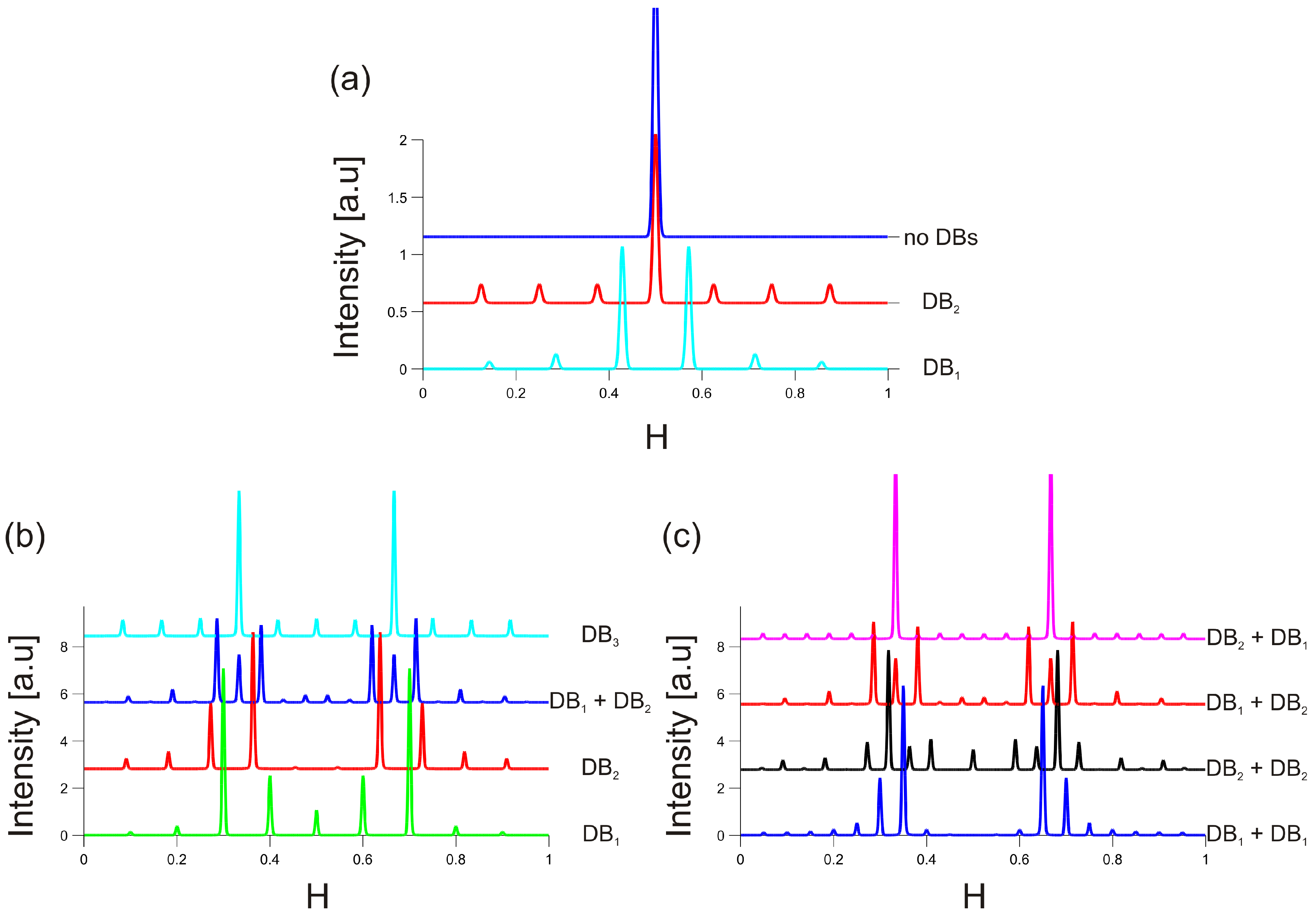
2.4. Two-Fold Periodicity

As discussed above, the most simple model for researching the effects of domain boundaries on the diffraction pattern is a surface reconstructed with a two-fold periodicity. Taking a closer look at its possible binary configurations, it becomes apparent that it is sufficient to assume one type of domain
D 1 = [ 1 0 ] ,
and two types of domain boundaries
D B 1 = [ 0 ] or D B 2 = [ 0 0 ] .
Figure 1a shows the diffraction pattern for a perfect two-fold periodicity (blue). As expected, a superstructure peak at H 1 n o m = 1/2, induced by the two-fold periodicity, arises. On one hand, a spot splitting (cyan) of this very peak takes place if DBs of type D B 1 (w = 1) are introduced between adjacent domains (here: N = 3 ). As mentioned above, strong diffraction peaks are only observed at positions H n = n / ( 2 N + 1 ) with n = N and n = N + 1 due to the structure factor S ( D ) ( H ) emphasizing diffraction peaks close to H 1 n o m = 1/2. Thus, the spot splitting is Δ H = 1 / ( 2 N + 1 ) .
On the other hand, the former superstructure peaks (red) reappear at H 1 n o m = 1/2 if DBs of type D B 2 (w = 2) separate domains of two-fold periodicity. Here, the domain boundaries cause the formation of satellite peaks at Δ H = ± 1 / ( 2 N + 2 ) with respect to the original superstructure diffraction peak at H 1 n o m = 1/2.
This very property of spot splitting of the superstructure peak versus satellite formation is equivalent to the observation for atomically stepped surfaces. At out-of-phase diffraction condition K = 2 π n / d , on one hand, one obtains an equally splitted (00) diffraction peak for a regularly stepped surface with mono atomic steps due to destructive interference between adjacent terraces of width N t (in multiples of the lattice constant a). Here, d and K denote the step height and the vertical scattering vector, respectively. However, it has to be noted that the spot splitting Δ H here is exactly 1/ N t since the step height does not contribute because the defect “atomic steps” is perpendicular to the lateral scattering vector H. In contrast to this, as mentioned above, the width of the DB contributes to the spot splitting due to its lateral character.
On the other hand, no spot splitting is observed at out-of-phase condition if the surface has atomic steps of double height 2d since the interference between adjacent terraces is constructive (effective in-phase condition) in this case. Instead, the (00) diffraction does not show any evidence for the stepped surface.
These out-of-phase and in-phase characters of atomic steps can also be assigned to the different DBs. The spot splitting for D B 1 is due to destructive interference between adjacent domains while the sharp peak at the nominal superstructure peak position for D B 2 is due to constructive interference. Therefore, D B 1 is an anti-phase domain boundary (APDB) with relative phase shift Δ φ 1 = 2 π w / p = π while D B 2 may be called an in-phase domain boundary (IPDB) due to the relative phase shift Δ φ 2 = 2 π w / p = 2 π .
Here, we like to mention that the sharp peak form of all superstructure peaks is caused by our supercell ansatz. If the domain widths follow some width distribution, these peaks are broadened and the broadening increases with increasing distance to the nominal superstructure diffraction peak at H n n o m = n / p , as will be shown in another contribution [13].

2.5. Three-Fold Periodicity

In principle, there are six different types of domains within the binary surface technique for the three-fold reconstructed surface. For reasons of simplicity, however, we only consider two domain types in the following:
D 1 = [ 1 0 0 ] and D 2 = [ 0 1 0 ] ,
and, from the multitude of domain boundaries, only the types
D B 1 = [ 0 ] , D B 2 = [ 0 0 ] or D B 3 = [ 0 0 0 ] .
Thus, most notably, the domain boundaries can assume different sizes (w = 1, 2 or 3).
Figure 1b exemplarily shows the diffraction pattern for the domain D 1 (here: N = 3) and the domain boundaries D B 1 (green), D B 2 (red) and D B 3 (cyan). Similar to the former results for the surface with two-fold periodicity, we obtain split superstructure spots for short and intermediate DBs, namely D B 1 (w = 1, green) and D B 2 (w = 2, red), respectively. The magnitude of the splitting is equal to the value expected by applying Equation (8). For the long boundary D B 3 (w = 3, cyan), however, the superstructure diffraction peak is not split but shows satellites separated as expected from Equation (8).
In contrast to the spot splitting for the surface with two-fold periodicity, however, the intensities of both diffraction peaks differ due to different distances to the nominal peak position H n n o m = n / 3 for the surface without domain boundaries. Therefore, the structure factor S ( D ) ( H ) of the domain modifies the intensity of the peaks.
The distances of these peaks with respect to the nominal peak obtained for the defect-free structure either exhibit a ratio of 1 : 2 or vice versa depending on the size w of the domain boundary. This can easily be explained within the supercell model considering, e.g., the peaks close to H 1 n o m = 1 / 3 . Here, one has to regard the supercell peaks H N and H N + 1 . For these peaks, the distances Δ H N and Δ H N + 1 with respect to H 1 ( n o m ) = 1 / 3 are
| Δ H N + 1 | | Δ H N | = 3 w w ,
which explains the result of | Δ H N + 1 | : | Δ H N | = 2 : 1 for w = 1 and 1 : 2 for w = 2 independent of the individual domain size N for the case at hand.
In addition, Figure 1b shows the case of alternation (blue) of D B 1 (w = 1) and D B 2 (w = 2) if the type of domain D 1 (N = 3) does not change. It becomes apparent that, in this case, the diffraction peaks at the nominal positions ( H 1 n o m = 1/3 or H 2 n o m = 2/3) are still present while additional satellite peaks are created due to the presence of domain boundaries. Due to the alternation of the DBs with different size, the next-next-neighbor domains are shifted relatively by w 1 + w 2 = 3 . Thus, next-next-neighbor domains interfere constructively.
This means that there are only two types of phase shifts ( Δ φ 1 = 2 π / 3 , Δ φ 2 = 4 π / 3 ) for adjacent domains. Consequently, these two domains cannot interfere completely destructively at the nominal position of the perfectly three-fold periodicity, and thus an additional peak emerges in the diffraction pattern. Furthermore, the split peaks are now located at equal distances from the nominal position and consequently show a mostly symmetric intensity distribution. This is opposed to the situation for only one type of domain boundary where there are all three types of phase shifts ( Δ φ 1 = 2 π / 3 , Δ φ 2 = 4 π / 3 and Δ φ 3 = 2 π ) that cancel out each other at the nominal spot position.
This effect for alternating DBs can also be treated in a different way. Indicating different DBs by different colours (green, red) the sequence
[ . . . | 100 | 100 | 100 | 0 | 100 | 100 | 100 | 00 | . . . ]
just discussed can also be rewritten as
[ . . . | 100 | 100 | 100 | 010 | 010 | 010 | 000 | . . . ]
introducing the domain type D 2 combined with the D B 3 . Thus, the length of periodicity is 2 N p + w and one has domain boundaries without anti-phase character. Consequently, there is a diffraction peak at the nominal position combined with satellites at Δ H = ± 1 / ( 2 · 3 N + 3 ) with almost doubled periodicity length Γ = 2 · 3 N + 3 .
As just introduced, not only the domain boundaries can be alternated but the domains themselves as well
[ . . . | D 1 ( N 1 ) | D B k | D 2 ( N 2 ) | D B l | . . . ] .
To keep it simple, Figure 1c shows only D 1 alternating with D 2 for every combination of the domain boundaries D B 1 (w = 1) and D B 2 (w = 2) with themselves and each other. If both domain boundaries exhibit equal length (e.g., D B k = D B l = D B 1 (w = 1), see Figure 1c, blue), the magnitude of the spot splitting decreases to half of the previous value. This also reflects the doubled periodicity induced by alternating different domains.
If domain boundaries of different sizes are alternated, however, an additional effect occurs. If we assume in the following the alternating domains D 1 (blue) and D 2 (black) as well as domain boundaries D B k = D B 1 (w = 1, green) and D B l = D B 2 (w = 2, red) for example (see Figure 1c, red), the following sequence is found in the binary array:
[ . . . | 100 | 100 | 100 | 0 | 010 | 010 | 010 | 00 | . . . ] .
Alternatively, this very sequence can be rewritten by rearranging the domain and domain boundaries:
[ . . . 100 | 100 | 100 | 00 | 100 | 100 | 100 | 0 | . . . ] .
This means that the two-domain two-domain-boundary model decomposes into a one-domain two-domain-boundary model with the following configuration D i = D j = D 1 (w = 1), D B k = D B 2 and D B l = D B 2 (w = 2). Consequently, the diffraction pattern is analogous to the diffraction pattern depicted in Figure 1b, blue. If we consider the configuration D i = D 1 (blue), D j = D 2 (black), D B k = D B 2 (w = 2, green) and D B l = D B 1 (w = 1, red) (see Figure 1c, magenta)
[ . . . | 100 | 100 | 100 | 00 | 010 | 010 | 010 | 0 | . . . ] ,
you can find the following equivalent expression
[ . . . | 100 | 100 | 100 | 000 | 100 | 100 | 100 | . . . ] ,
with identical domains D 1 and D B k = D B 3 (w = 3). This means that the second domain boundary D B l vanishes and the first domain boundary D B k is commensurable with the three-fold periodicity (e.g., no phase shift), explaining nicely that a quasi-perfect three-fold periodicity can be observed in the diffraction pattern even though domain boundaries are present.
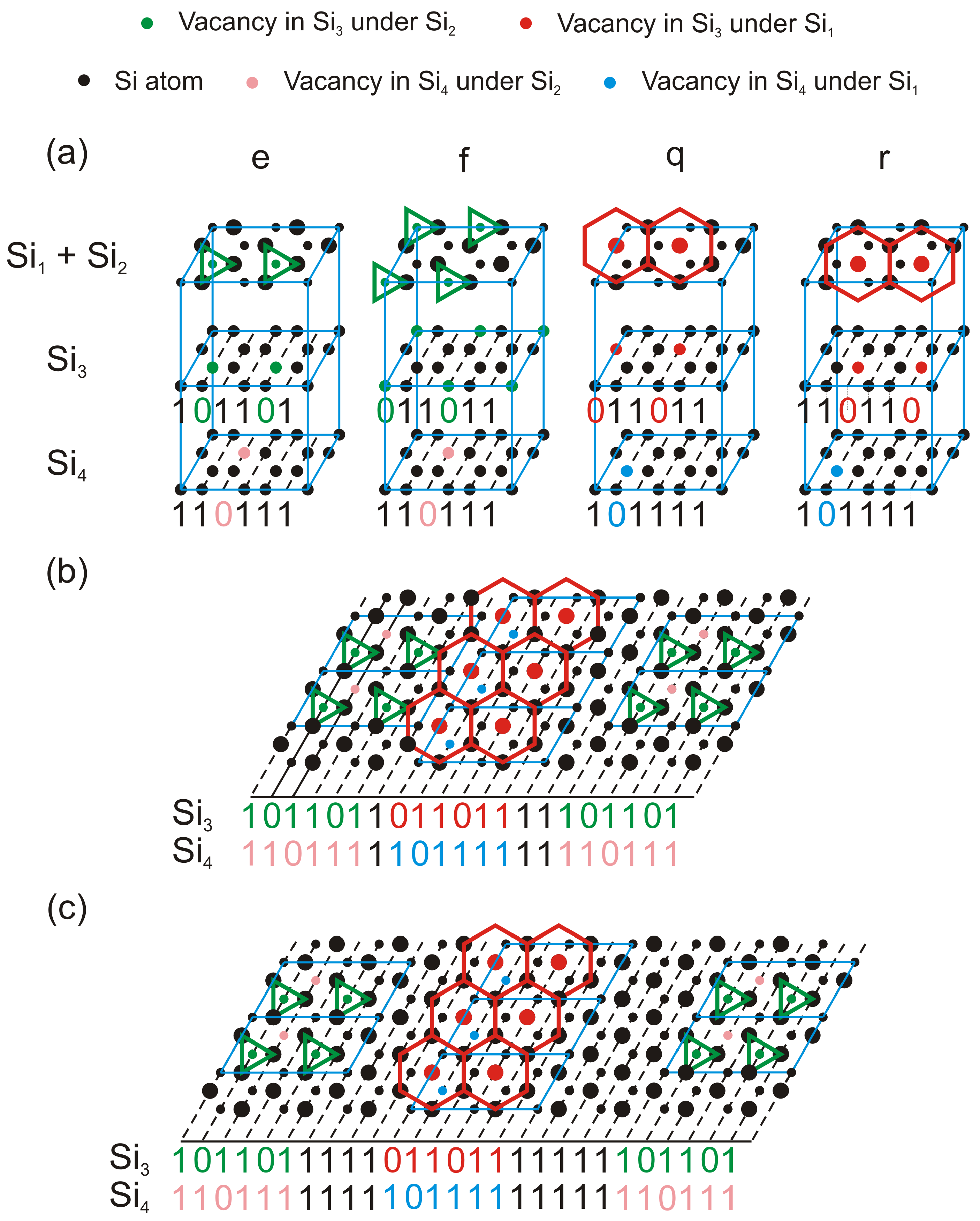
2.6. 2 3 × 3 R 30 Reconstruction

In this section, the diffraction pattern of the 2 3 × 3 R 30 reconstruction of (Dy, Tb) on Si(111) [11] will be discussed as an example demanding a detailed analysis in the framework presented above since the effective unit cells are too large to perform standard diffraction analysis.
The atomic structure of the reconstruction is rather complex (see Figure 2 as analyzed in [11] combining density functional theory (DFT), STM and LEED. It is composed of three Si layers: one buckled Si bilayer (Si 1 , Si 2 ), and two silicene-like (hexagonal, flat) layers (Si 3 , Si 4 ) that host a network of Si vacancies. The three Si layers are separated by rare earth layers. Experimental evidence shows that the Si 3 layer exhibits a 3 × 3 R 30 reconstruction and the Si 4 layer exhibits a 2 3 × 3 R 30 reconstruction due to periodically arranged Si vacancies. The Si 4 layer has one vacancy per 2 3 × 3 R 30 unit cell while the Si 3 has two. Additionally, the vacancies in both layers are not collinearly arranged (cf. colored positions in Figure 2).
There is evidence that two different types of domains alternate across the 2 3 -direction of the unit cell. Indeed, DFT calculations show that there are four stable structure models (e, f, q, r, see Figure 2) with different arrangements of the vacancies but comparable formation energies. The models (e, f) represent one type of domain D 1 and models (q, r) the other type D 2 . Furthermore, the two different types of domains are separated by DBs because a splitting of odd order diffraction spots in 2 3 -direction is observed when LEED experiments are performed. As compared to a perfect silicene layer, the DFT calculations additionally predict a tensile strain of the silicene-like Si 3 and Si 4 layers of the unit cell in 2 3 -direction due to the Si vacancies. This strain can only be compensated if the density of vacancies is decreased, resulting in a formation of DBs containing no vacancies. Furthermore, STM experiments show that the growth in 3 -direction is only limited by the step edges. Consequently, the structure exhibits striped domains with a high aspect ratio, making it a quasi-one-dimensional structure. Combining all information given above, it can be postulated that the spot splitting is explained by a supercell of the following structure
[ . . . | D 1 ( e / f , N 1 ) | D B 1 | D 2 ( q / r , N 2 ) | D B 2 | . . . ] ,
meaning that a domain of D 1 (either e or f) of a size N 1 alternates with a domain of D 2 (either q or r) of a size N 2 . Additionally, the two types of domains are separated by DBs where a transition from one type of domain to the other ( D 1 D 2 ) does not necessarily have to be the same as the reversed transition ( D 2 D 1 ), resulting in two different domain boundaries D B 1 and D B 2 .
However, experimentally, neither the width nor the exact orientation of the different types of domains to each other can be determined by STM. Additionally, the size of the supercell (multiple 2 3 unit cells) makes DFT calculations prohibitive. Thus, in order to gain a deeper insight into the arrangement of the two types of domains, kinematical diffraction simulations are performed.
Since both the Si bilayer (Si 1 , Si 2 ) and the rare earth layer exhibit a 1 × 1 reconstruction, they do not contribute to the superstructure diffraction peaks and can consequently be ignored for their analysis. The two-dimensional atomic structure of the 3 × 3 R 30 reconstructed Si 3 layer and the 2 3 × 3 R 30 reconstructed Si 4 layer can be transformed into one-dimensional structures by projecting them onto the crystallographic axis of the 2 3 -direction (see Figure 2), in which the two types of different domains (separated by DB) alternate. However, in order to be able to account for the different positions of the vacancies in the unit cell for both types of domains, the lattice constant a must be chosen equal to the lateral distance between Si atoms rows in Si(111), i.e., a = a 0 3 / 3 (with a 0 = 3.84). Figure 2 shows the sequences of binarizations used to perform these calculations.
In order to generate the general diffraction pattern of this two layered structure, the vertical phase shift needs to be taken into account by
| G ( H , L ) | 2 = G Si 3 ( H ) + G Si 4 ( H ) exp ( 2 π i L ) 2 .
Here, G ( H , L ) is the lattice factor as a function of out-of-plane scattering vector K = 2 π L /d (where d is the layer spacing), and G Si 3 and G Si 4 are the lattice factors (Fourier transforms) of the binary arrays of the respective layers. However, for the following only, calculations for integer values of L are performed. Hence, the diffraction pattern equates to the absolute square of the sum of both of the Fourier transforms due to constructive interference between domains
| G ( H ) | 2 = G Si 3 ( H ) + G Si 4 ( H ) 2 .
The simplest way to have D 1 and D 2 alternate is to alternate only two models that belong to different types of domains separated by two types of anti-phase domain boundaries creating the following type of supercell
[ . . . | D 1 ( e , N 1 ) | D B 1 | D 2 ( q , N 1 ) | D B 2 | . . . ] .
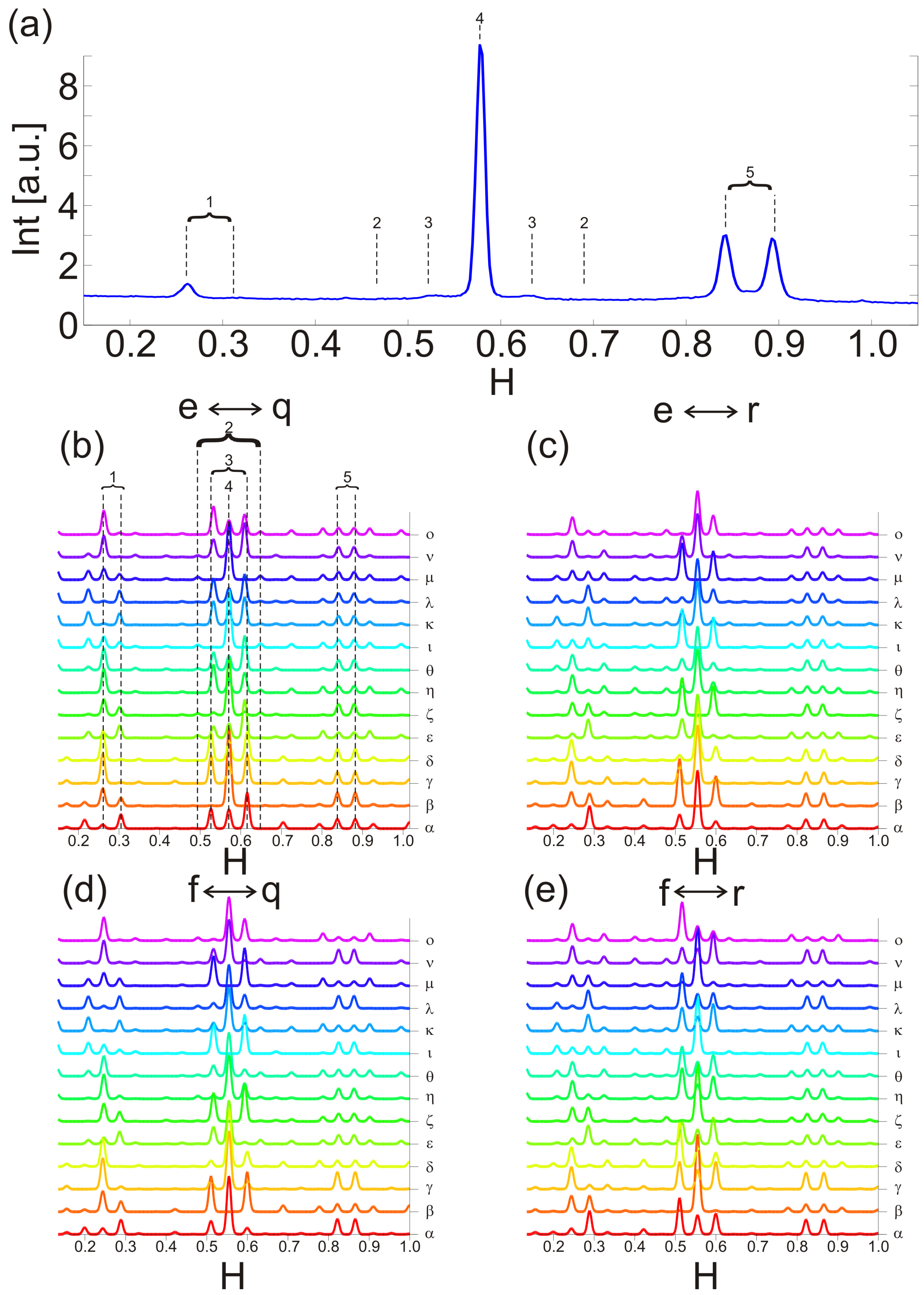
In LEED experiments, one observes that only peaks of odd order are split (see Figure 3a, cf. [11]). Therefore, taking into account our previous considerations, it can be deduced that the combined size w 1 + w 2 of the domain boundary must be an odd multiple of a 0 3 since one would observe a splitting of the even order superstructure spots otherwise. Translated to the binary description, this means that the width of the complete domain boundary w t o t must be equal to
w t o t = w ( D B 1 ) + w ( D B 2 ) = 6 N + 3 , N N .
However, a priori, there is no knowledge about the size of the individual domain boundaries. Therefore, on one hand, Figure 3a shows the experimentally received diffraction pattern. On the other hand, Figure 3b–e show the diffraction patterns for the coherent superposition of the layers Si 3 and Si 4 for N 1 = N 2 = 3 and w = 3, 9 for all possible domain boundaries.
In total, five different features can be identified in the diffraction patterns. Feature 1 corresponds to the split first order, feature 4 to the second order spot and feature 5 to the split third order spot of the base ( 2 3 × 3 ) periodicity. Features 2 and 3 can be interpreted as the first order (feature 3) and second order (feature 2) satellites of the second order diffraction spot. Their positions can be explained by the average periodicity of the supercell
Γ = N ( D 1 ) 2 3 + w ( D B 1 ) 3 / 3 + N ( D 2 ) 2 3 + w ( D B 2 ) 3 / 3
via Equation (8). Table 1 exemplarily shows the assignment of the different features observed in Figure 3 for the respective models (α through o) for the combination of the models e and q.
Comparing the experimental features (cf. Figure 3a) to the features observed in the simulated diffraction patterns (cf. Figure 3b), it becomes obvious that only model β shows the observed diffraction pattern analogous to the experimental diffraction pattern (only splitting of odd order spots, no additional features). Taking a look at the particular binary configuration for Si 3
[ . . . 101101 | 1 | 011011 | 011011 | 011011 | 11 | 101101 | 101101 . . . ] , [ . . . 10110 | 110110 | 110110 | 110110 | 111 | 110110 | 110110 | 1 . . . ] ,
and Si 4
[ . . . 110111 | 1 | 101111 | 101111 | 101111 | 11 | 110111 | 110111 . . . ] , [ . . . 11011 | 111011 | 111011 | 111011 | 111 | 111011 | 111011 | 1 . . . ] ,
it can be found that, for this particular arrangement of domain boundaries and domains, the binary sequences decomposes into simpler systems. For the Si 3 layer, one receives a 3 reconstructed array with only one domain and a commensurate domain boundary explaining a diffraction pattern that is very close to a 3 periodicity. For the Si 4 layer, one receives a 2 3 reconstructed array with a single domain and one type of DB resulting in a symmetric splitting of (basically only) odd order diffraction spots. For every other combination of domains and domain boundaries, only either the binary sequence of layer Si 3 or Si 4 or none of them decompose into a one-domain one-domain-boundary system. Hence, their diffraction patterns exhibit additional features that are in stark contrast to the experimental findings.
The interference between both layers also plays a significant role. Due to the lateral displacement of the vacancies in both layers (Si 3 , Si 4 ), an intensity asymmetry of the first order and fifth order (split) spots is induced [11].
Analyzing all diffraction patterns of the other combinations of models in the same fashion, only one additional model agreeing with the experimental evidence can be found, model β (cf. Figure 3d) for the combination of models f and r, which, incidentally, exhibits the same anti-phase boundaries as for the combination of models e and q.
This means that, in order to explain the experimental diffraction pattern, only the anti-phase domain boundaries D B 1 = [1] and D B 2 = [1 1] may be present. Additionally, only transitions from eq and transitions from fr may occur, leading to the interpretation that these transitions must be energetically more favorable than the other possible transitions. However, it is difficult to assess this hypothesis by conventional methods (e.g., DFT) due to the large unit cells involved. Having identified the most probable structure of the supercell, the mean domain size Γ s c of the supercell can be determined from the spot splitting Δ H
Γ s c = N 1 + w 1 + N 2 + w 2 = 11
given in unit cells of the 2 3 periodicity, agreeing nicely with the experimental evidence obtained by STM. The analysis can be refined if one takes into account domain size distributions to analyze the profiles of the split superstructure spots as presented elsewhere [13].
Additionally, we like to mention that our calculations are on the same footing as the kinematical diffraction theory calculations for the Pt(111)- 3 × 3 R 30 -Xe system with domain walls [14]. Here, different diffraction patterns are reported for the striped domains depending on the width of the domain walls/boundaries. However, in contrast to the Xe/Pt(111) system, where the DBs are not orientated alongside either 3 -direction, the DBs in the system at hand are orientated alongside the 3 -direction of the unit cell. Consequently, the diffraction patterns studied here only show non-integer diffraction spots along the 2 3 -direction. This result is opposed to the situation for the Xe/Pt(111) system, where additional triangularly arranged triplet diffraction peaks are reported surrounding the 3 × 3 R 30 diffraction peaks. Similar effects of triangularly arranged diffraction split peak triplets are also reported for Pb/Si(111) [8,9]. Additionally, we like to emphasize that the diffraction pattern of the Si(111)- 2 3 × 3 R 30 - RE 12 Si 21 is more complicated compared to Pt(111)- 3 × 3 R 30 -Xe by the fact that different types of DBs alternate, increasing the number of possible diffraction spots observed.

3. Conclusions

Calculating diffraction patterns and applying the binary surface technique, we were able to show the influence of domain boundaries on the diffraction pattern for selected structures. Motivated by the formation of striped domains, these calculations were performed for one-dimensional systems in the framework of the kinematical diffraction theory using the supercell approach. Depending on the width of the domain boundaries and combining different types of domains and domain boundaries, a plethora of different features can be observed in the diffraction patterns. The analysis of the diffraction pattern obtained from these binary sequences lastly enabled us to identify the structure and width of the domain boundaries of the 2 3 × 3 R 30 reconstruction of rare-earth silidices (Dy, Tb) on Si(111). Future works will consider the distribution of domain widths and study the effect on spot profiles.
Part of this work has been presented at the international conference on Atomically Controlled Surfaces Interfaces and Nanostructures ACSIN2016 held in Frascati, Rome Italy from 9 Oct 2016 to 15 Oct 2016 [15].

Acknowledgments

The authors would like to thank the Deutsche Forschungsgemeinschaft through FOR 1700, project E2, for financial support.

Author Contributions

F.T. and J.W. developed the models, calculated the patterns and wrote the paper. Both authors have read and approved the final manuscript.

Conflicts of Interest

The authors declare no conflict of interest. The founding sponsors had no role in the design of the study; in the collection, analyses, or interpretation of data; in the writing of the manuscript, and in the decision to publish the results.

Abbreviations

The following abbreviations are used in this manuscript:
LEEDLow energy electron diffraction
SPA-LEEDSpot-profile analysis-Low energy electron diffraction
DBDomain boundary
APDBAnti-phase domain boundary
SSSuperstructure
STMScanning tunneling microscop
DFTDensity functional theory

References

  1. Pendry, J.B. Low Energy Electron Diffraction; Academic Press: London, UK, 1974. [Google Scholar]
  2. Van Hove, M.A.; Tong, S.Y. Surface Crystallography by LEED: Theory, Computation and Structural Results; Springer: Berlin, Germany, 1979. [Google Scholar]
  3. Clarke, J.L. Surface Crystallography: An Introduction to Low Energy Electron Diffraction; Wiley: Chichester, UK, 1985. [Google Scholar]
  4. Henzler, M. Electron Diffraction and Surface Defect Structure. In Electron Spectroscopy for Surface Analysis; Ibach, H., Ed.; Springer: Berlin, Germany, 1977; pp. 117–149. [Google Scholar]
  5. Henzler, M. Defects in Surface Structure: Information by LEED. In Festkörperprobleme; Treusch, J., Ed.; Vieweg: Braunschweig, Germany, 1979; Volume 19, pp. 193–208. [Google Scholar]
  6. Henzler, M. Measurement of Surface Defects by Low-Energy Electron Diffraction. Appl. Phys. A 1984, 34, 205–214. [Google Scholar] [CrossRef]
  7. Horn-von Hoegen, M. Growth of semiconductor layers studied by spot profile analysis low energy electron diffraction—Part I. Z. Kristallogr. 1999, 214, 591–629. [Google Scholar]
  8. Petkova, A.; Wollschläger, J.; Günther, H.-L.; Henzler, M. Formation and commensurate analysis of “incommensurate” superstructures of Pb on Si(111). Surf. Sci. 2001, 471, 11–20. [Google Scholar] [CrossRef]
  9. Stepanovska, S.; Yakes, M.; Yeh, V.; Hupalo, M.; Tringides, M.C. The dense α-( 3 × 3 )Pb/Si(111) phase: A comprehensive STM and SPA-LEED study on ordering, phase transitions and interactions. Surf. Sci. 2006, 600, 1417–1430. [Google Scholar] [CrossRef]
  10. Saranin, A.A.; Lifshitz, V.G.; Bethge, H.; Kayser, R.; Klust, A.; Goldbach, H.; Wollschläger, J.; Henzler, M. Restructuring process of the Si(111) surface upon Ca deposition. Surf. Sci. 2000, 448, 87–92. [Google Scholar] [CrossRef]
  11. Timmer, F.; Oelke, R.; Dues, C.; Sanna, S.; Schmidt, W.G.; Franz, M.; Appelfeller, S.; Dähne, M.; Wollschläger, J. Strain-induced quasi-one-dimensional rare-earth silicide structures on Si(111). Phys. Rev. B 2016, 94, 205431. [Google Scholar] [CrossRef]
  12. Klasing, F. Indium on Silicon(111) Low-Energy Electron Diffraction Experiments and Simulations on the Striped (8 × 2) Surface Reconstruction and the (4 × 1) ↔ (8 × 2) Phase-Transition. Ph.D. Thesis, University of Duisburg-Essen, Duisburg, Germany, 2014. [Google Scholar]
  13. Timmer, F.; Wollschläger, J. Influence of the Distribution of Domains and Domain Boundaries of One-Dimensional Structures on Diffraction Peaks Profiles. Unpublished work. 2017. [Google Scholar]
  14. Zeppenfeld, P.; Kern, K.; David, R.; Comsa, G. Diffraction from domain-wall systems. Phys. Rev. B 1988, 38, 3918–3924. [Google Scholar] [CrossRef]
  15. Bianconi, A.; Marcelli, A. (Eds.) Atomically Controlled Surfaces Interfaces and Nanostructures; Superstripes Press: Rome, Italy, 2016.
Figure 1. (a) diffraction pattern of the perfect two-fold periodicity (blue) and after introduction of domain boundaries D B 1 (w = 1, cyan) and D B 2 (w = 2, red); (b) diffraction pattern of the three-fold periodicity for the D 1 domain and the domain boundaries D B 1 (green), D B 2 (red), D B 3 (cyan) and the alternation of D B 1 and D B 2 (blue); (c) diffraction patterns for the alternation of the domains D 1 and D 2 with the domain boundaries D B k = D B 1 and D B l = D B 1 (blue), D B k = D B 2 and D B l = D B 2 (black), D B k = D B 1 and D B l = D B 2 (red) and D B k = D B 2 and D B l = D B 1 (magenta).
Condensedmatter 02 00007 g001
Figure 2. (a) Schematic display of the structure model of the 2 3 × 3 R 30 reconstruction. There are four different energetically favorable models (e, f, q, r) that belong to two different types of domains. The models e and f make up the first type of domain where the vacancies in the Si 3 and Si 4 layer are located underneath Si atoms in the Si 2 layer, whereas the models q and r make up the second domain where the vacancies in the Si 3 and Si 4 layer are located underneath Si atoms in the Si 1 layer. Both models exhibit different structural motives in Scanning Tunneling Microscopy (STM) measurements [11], which are indicated here by green triangles and red hexagons. The binary sequences after the projection onto the relevant crystallographic axis of the different models for the layer Si 3 and Si 4 are given reflecting the fact that the Si 3 layer exhibits a ( 3 × 3 ) periodicity and the Si 4 layer exhibits a ( 2 3 × 3 ) periodicity. (b,c) example of two potential supercells [...|e| D B 1 |q| D B 2 |...] incorporating different sizes of DBs. (b) w ( D B 1 ) = 1 and w ( D B 2 ) = 2 and (c) w ( D B 1 ) = 4 and w ( D B 2 ) = 5. For reasons of better visibility, the supercells only contain one unit cell of the model e and q, respectively. However, in principle, the supercell can contain multiple unit cells of either model and the domain sizes can be obtained from the superstructure peak splitting.
Condensedmatter 02 00007 g002
Figure 3. (a) experimentally observed diffraction pattern along the 2 3 -direction; (be) diffraction pattern of the four models (eq, er, fq, fr) for all possible combinations of the anti-phase domain boundaries D B 1 and D B 2 for w ( D B 1 ) + w ( D B 2 ) = 3 or 9. The lateral scattering vector H is given in units of the silicon substrate. This means that the nominal first order diffraction spot is located at 1/(2 3 ) = 0.2887. Consequently, peaks of higher order are located at multiples of this alue. Additionally, only a part of the diffraction pattern is displayed for reasons of better visibility.
Condensedmatter 02 00007 g003
Table 1. Assignment of the five features observed in the simulated diffraction patterns (see Figure 3b) of the 14 models (α through o) for the combination of model e and q. Additionally, the width of both types of the DBs is displayed for the different models.
FeatureExperimentalαβγδϵζηθικλμνo
1
2
3
4
5
w ( D B 1 ) -01230123456789
w ( D B 2 ) -32109876543210

