Author Contributions
Conceptualization, T.L.; methodology, T.L.; software, T.L.; validation, T.L.; formal analysis, T.L.; investigation, T.L.; resources, T.L. and H.-P.L.; data curation, T.L.; writing—original draft preparation, T.L.; writing—review and editing, T.L. and H.-P.L.; visualization, T.L. and H.-P.L.; supervision, H.-P.L.; project administration, H.-P.L.; funding acquisition, H.-P.L. All authors have read and agreed to the published version of the manuscript.
Figure 1.
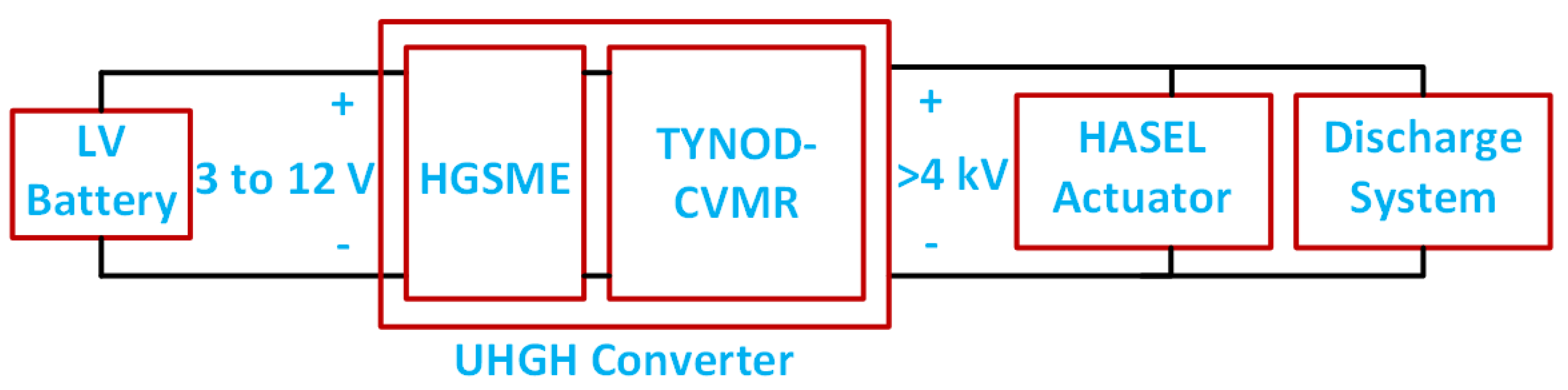
Actuation of HASEL with UHGH converters [
3].
Figure 1.
Actuation of HASEL with UHGH converters [
3].
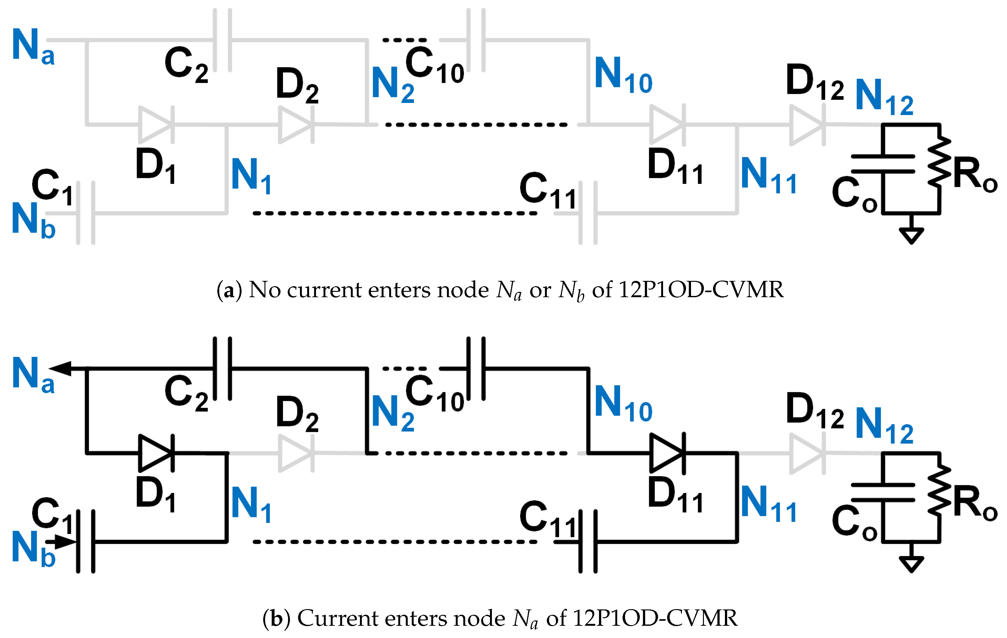
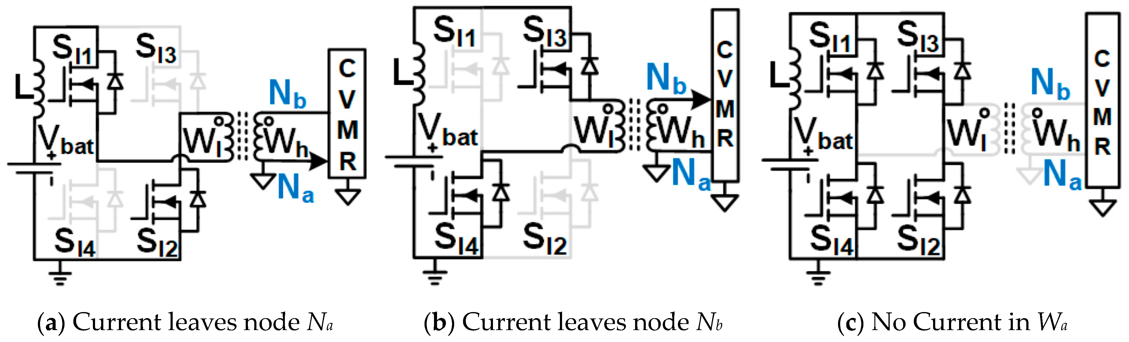
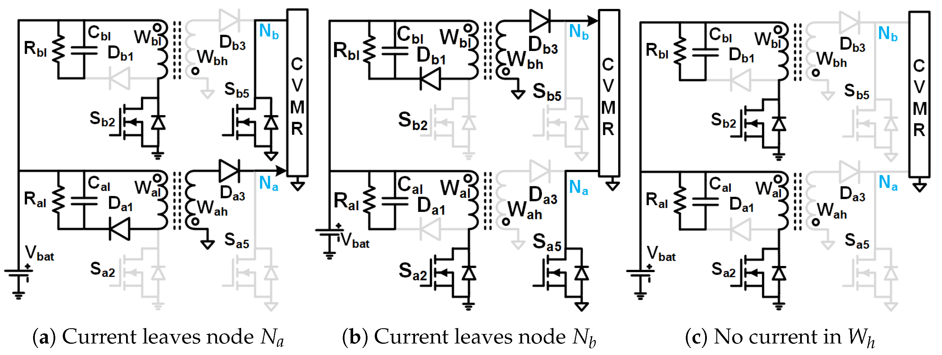
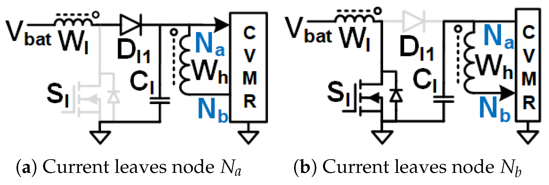
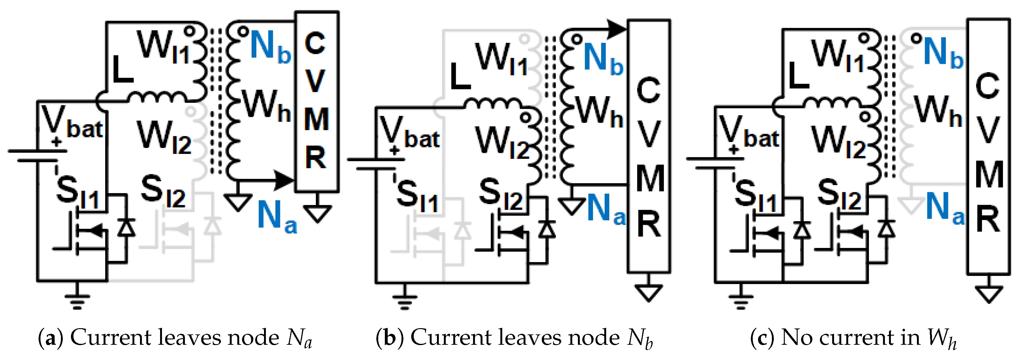
Figure 2.
Equivalent circuits describing the operation of the 12P1OD-CVMR part.
Figure 2.
Equivalent circuits describing the operation of the 12P1OD-CVMR part.
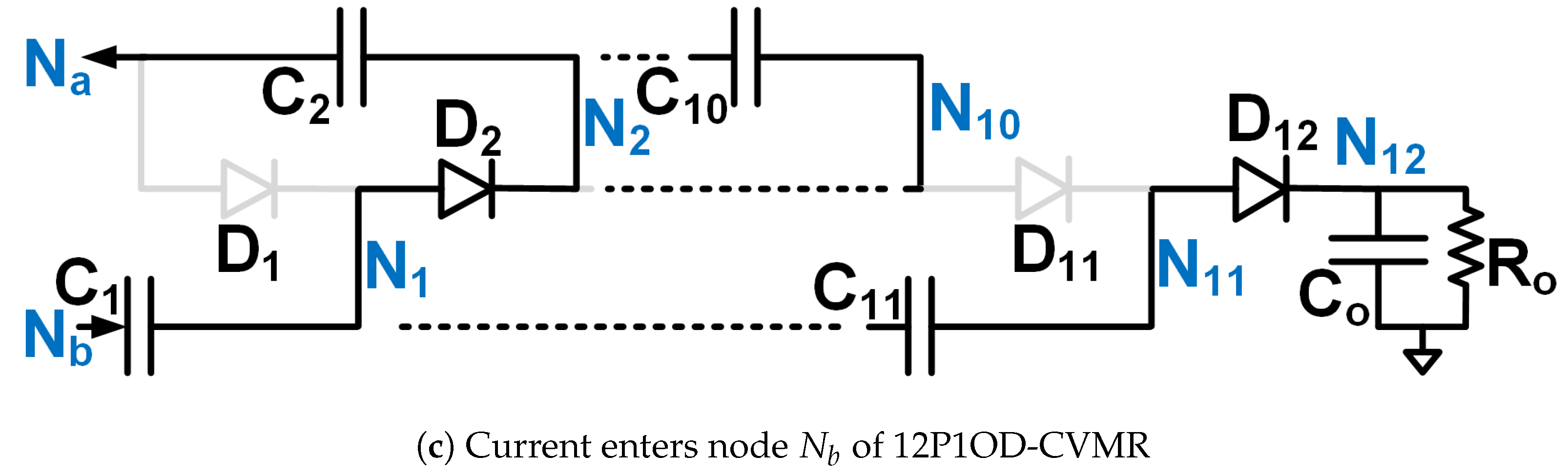
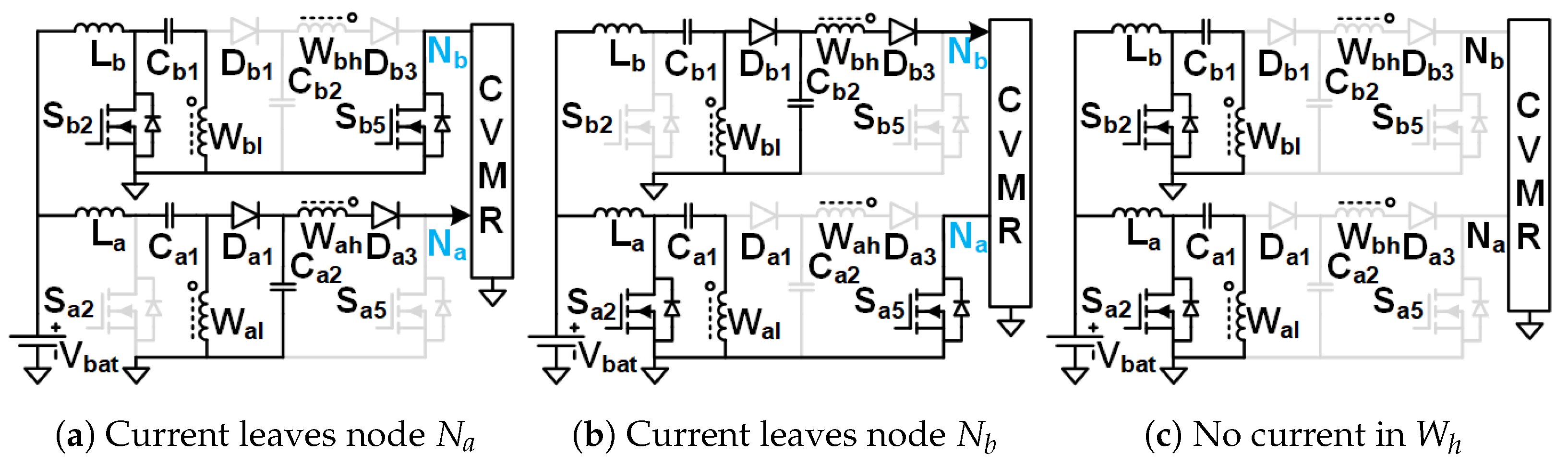
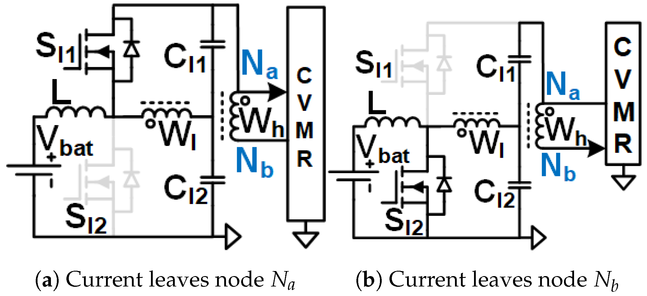
Figure 3.
Equivalent circuits describing the operation of the 12P2OD-CVMR part.
Figure 3.
Equivalent circuits describing the operation of the 12P2OD-CVMR part.
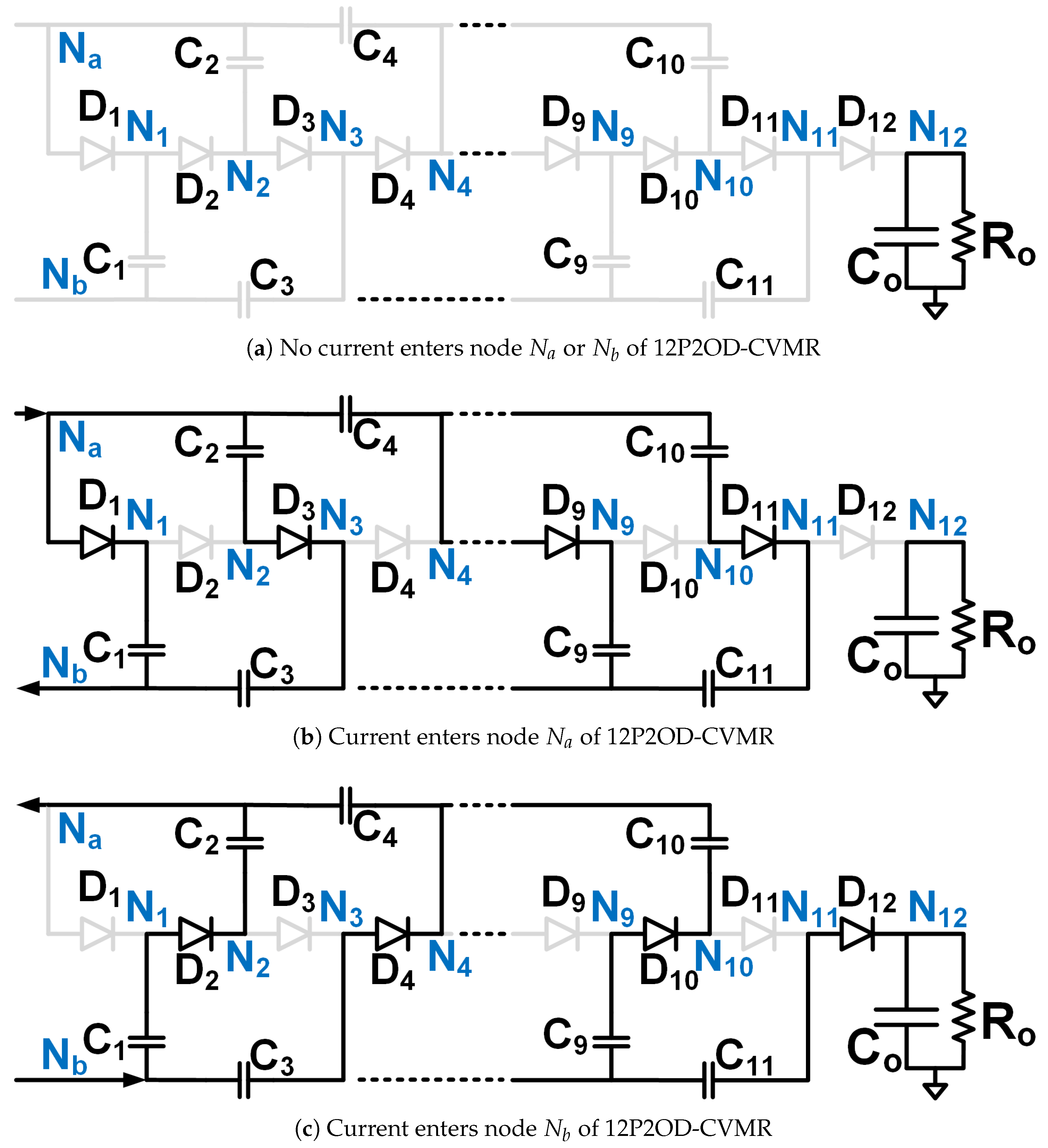
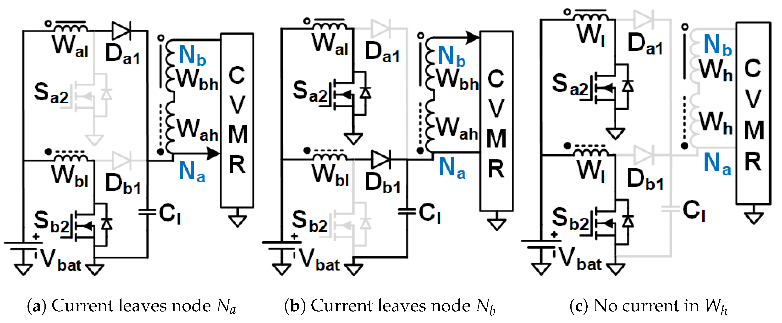
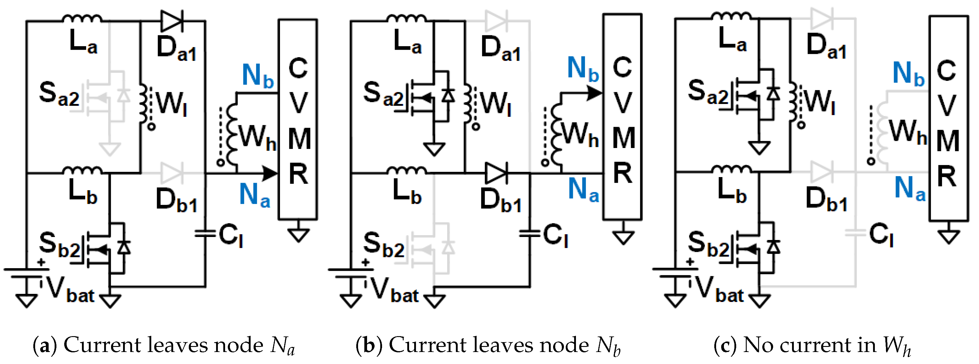
Figure 4.
Equivalent circuits describing the operation of the 12PDOD-CVMR part.
Figure 4.
Equivalent circuits describing the operation of the 12PDOD-CVMR part.
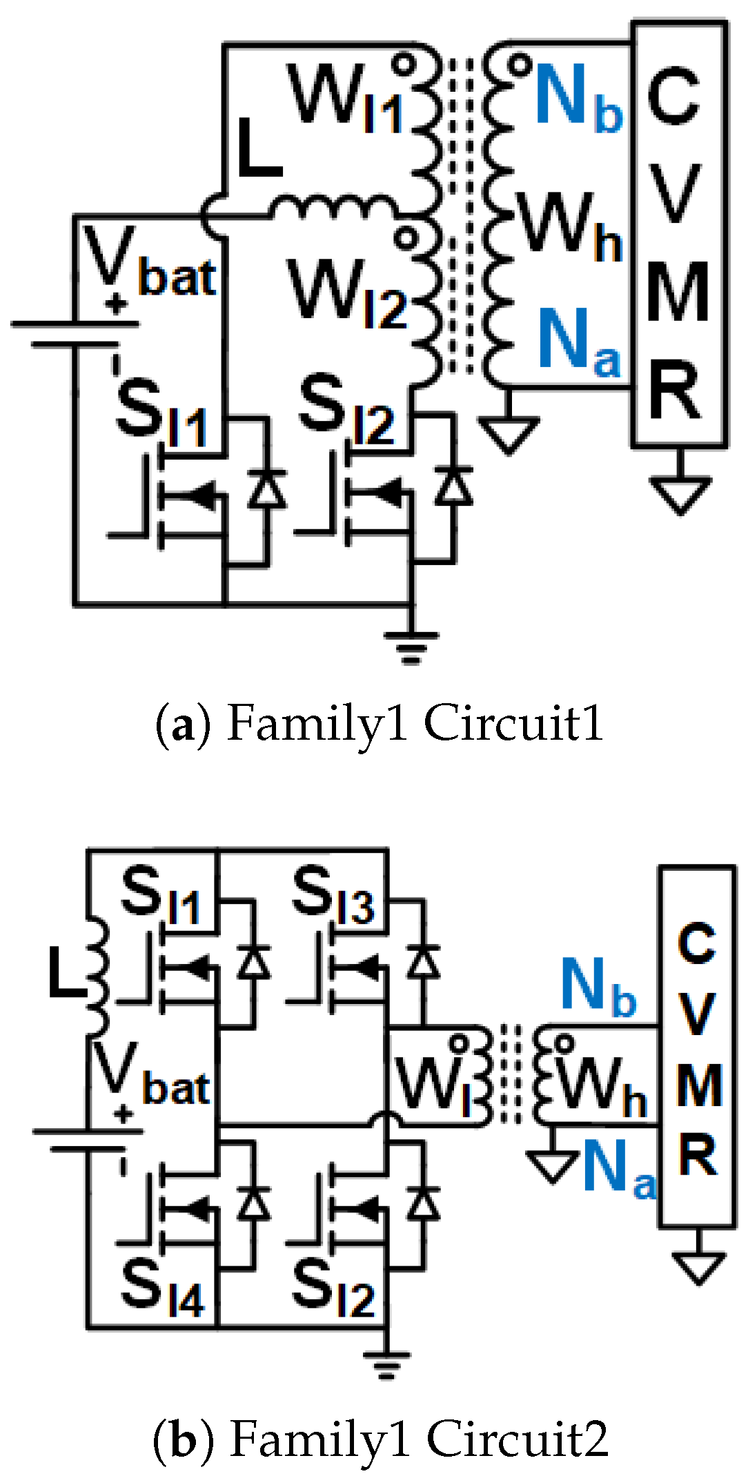
Figure 5.
UHGH converters of Family1.
Figure 5.
UHGH converters of Family1.
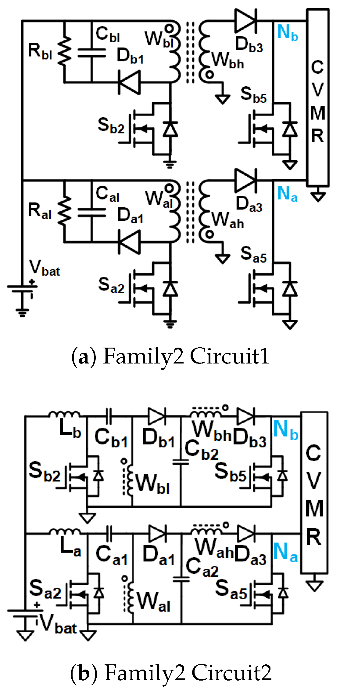
Figure 6.
UHGH converters of Family2.
Figure 6.
UHGH converters of Family2.
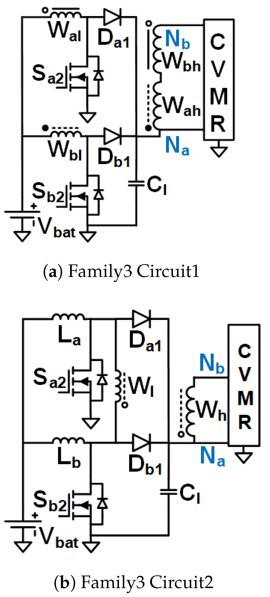
Figure 7.
UHGH converters of Family3.
Figure 7.
UHGH converters of Family3.
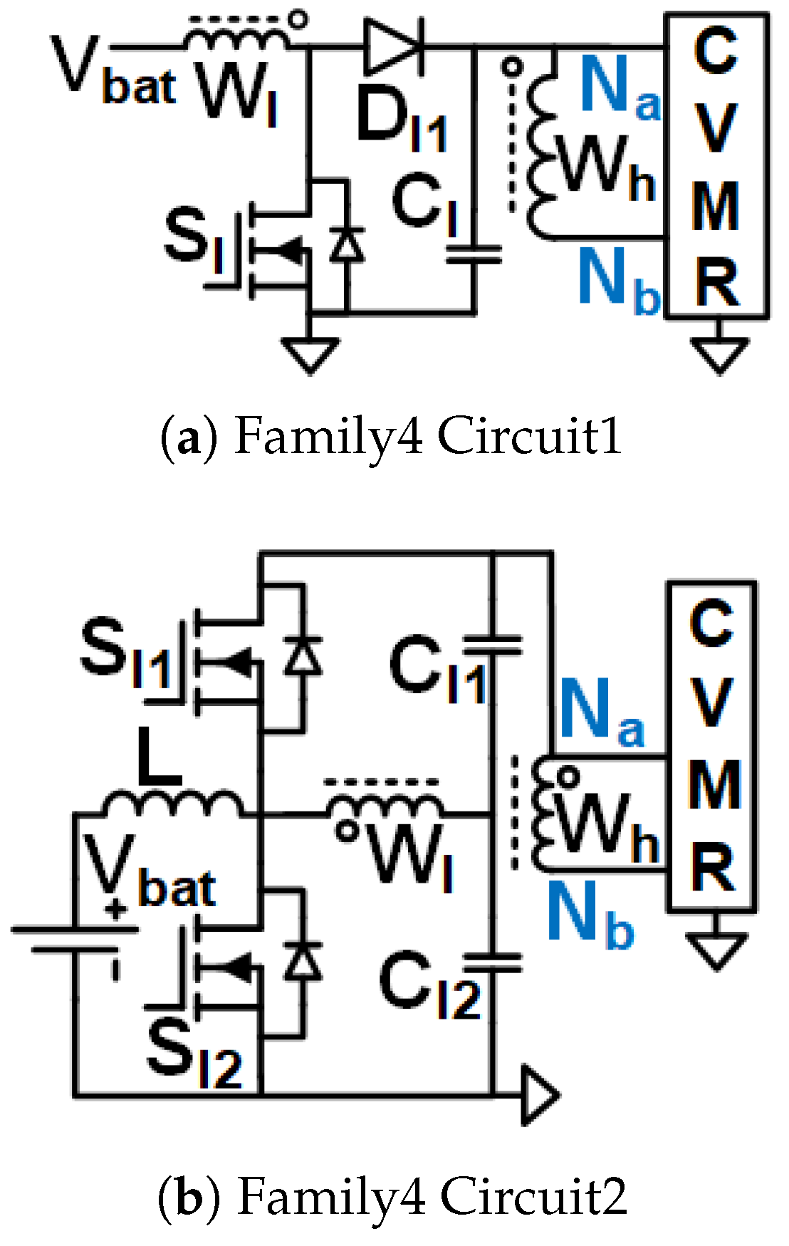
Figure 8.
UHGH converters of Family4.
Figure 8.
UHGH converters of Family4.
Figure 9.
Family1 Circuit1 modes.
Figure 9.
Family1 Circuit1 modes.
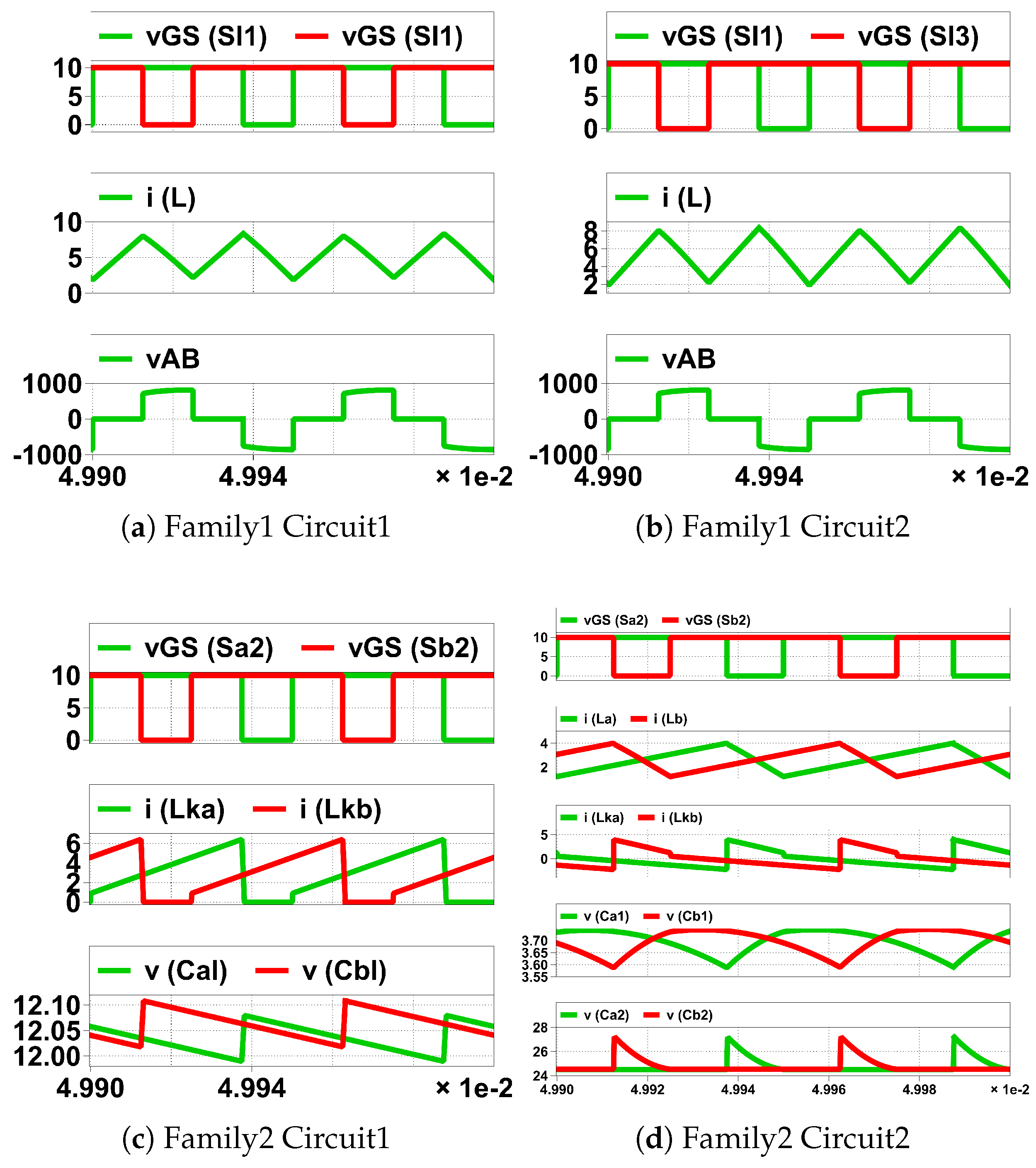
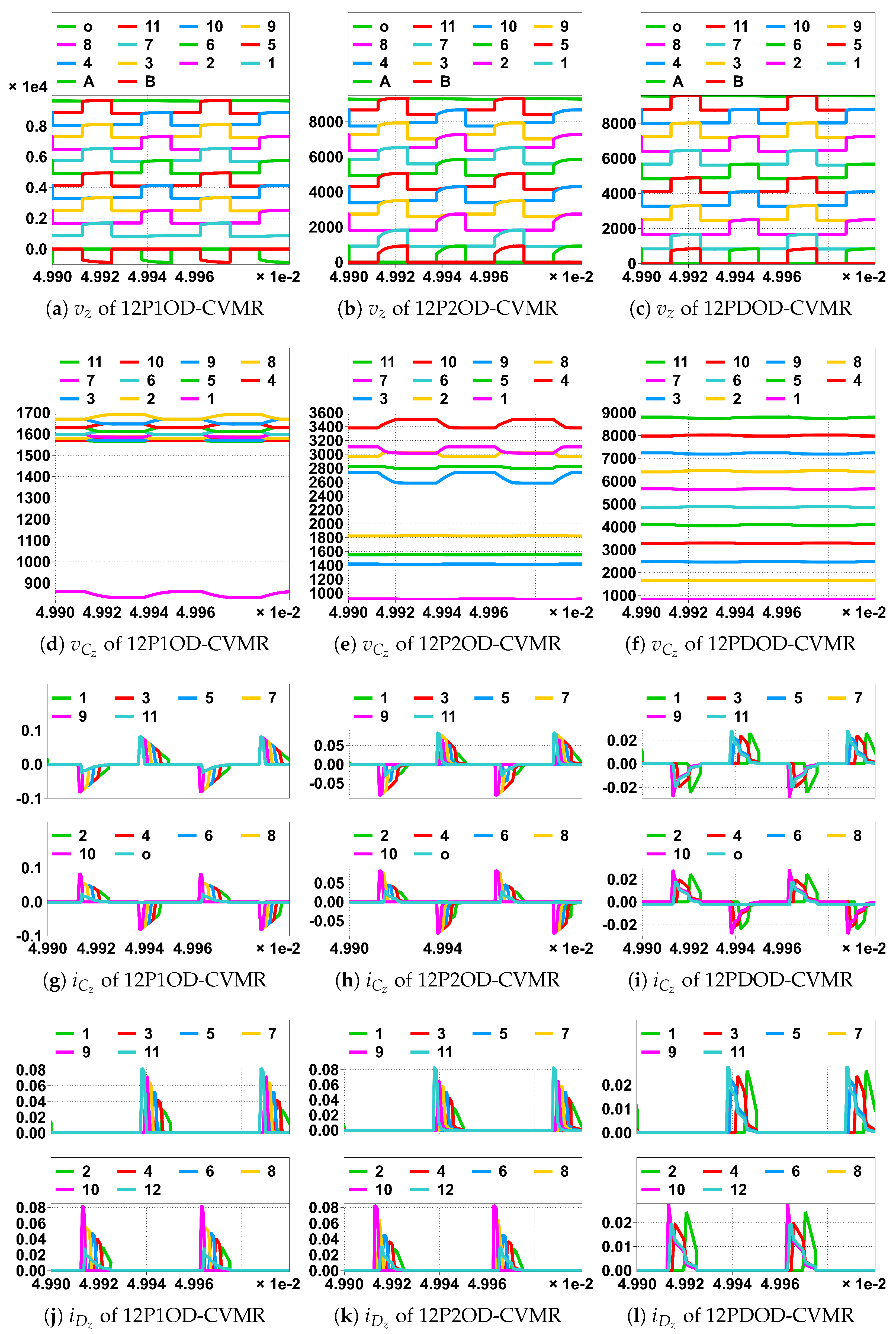
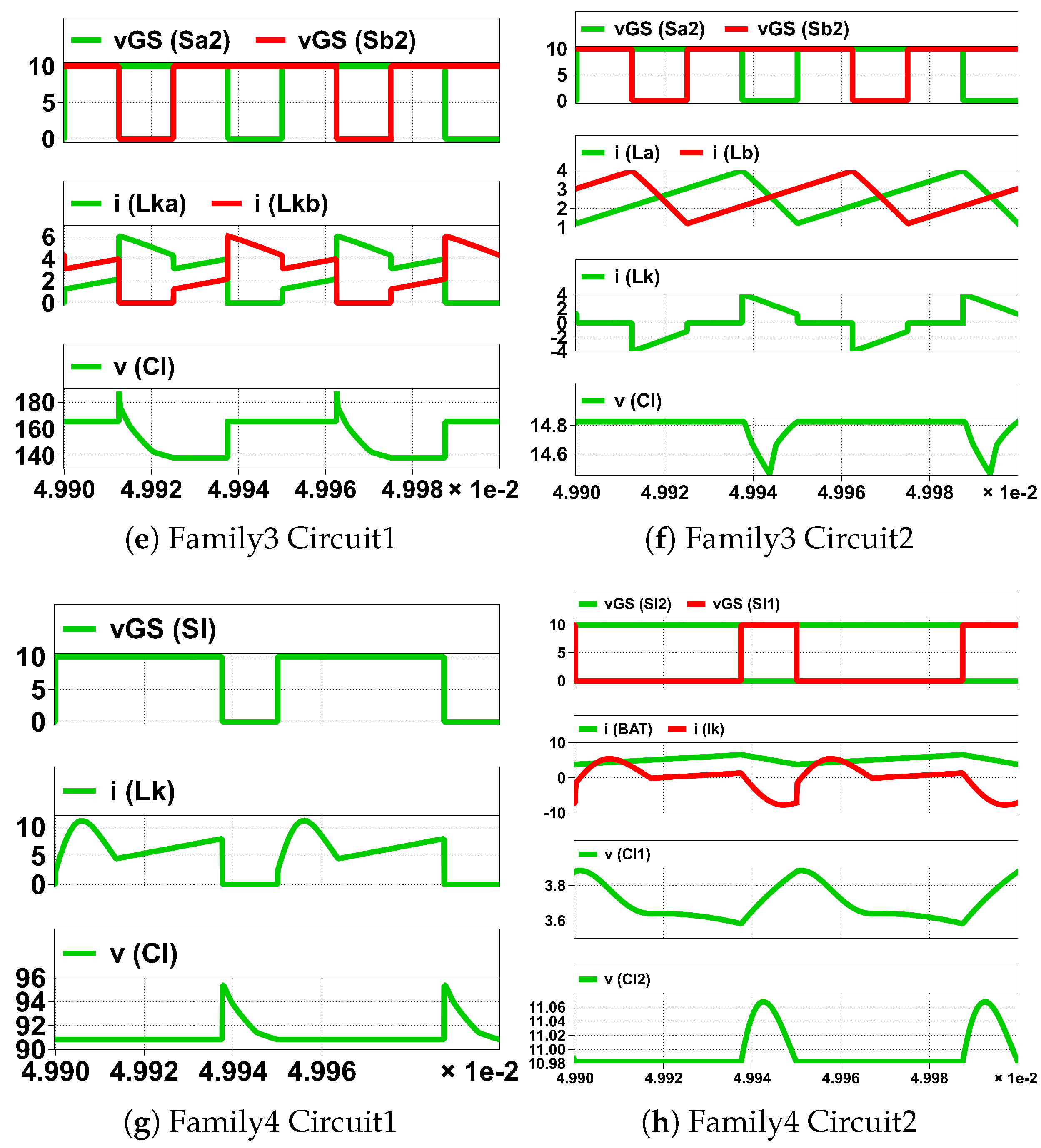
Figure 10.
Simulation of HGSME of the UHGH converters. In horizontal scale ×1e-2 means , unit is Second.
Figure 10.
Simulation of HGSME of the UHGH converters. In horizontal scale ×1e-2 means , unit is Second.
Figure 11.
Family1 Circuit2 modes.
Figure 11.
Family1 Circuit2 modes.
Figure 12.
Family2 Circuit1 modes.
Figure 12.
Family2 Circuit1 modes.
Figure 13.
Family2 Circuit2 modes.
Figure 13.
Family2 Circuit2 modes.
Figure 14.
Family3 Circuit1 modes.
Figure 14.
Family3 Circuit1 modes.
Figure 15.
Family3 Circuit2 modes.
Figure 15.
Family3 Circuit2 modes.
Figure 16.
Family4 Circuit1 modes.
Figure 16.
Family4 Circuit1 modes.
Figure 17.
Family4 Circuit2 modes.
Figure 17.
Family4 Circuit2 modes.
Figure 18.
Simulation of CVMR part of the UHGH converters of Family2; (legend number is the value of z). In horizontal scale ×1e-2 means , unit is Second.
Figure 18.
Simulation of CVMR part of the UHGH converters of Family2; (legend number is the value of z). In horizontal scale ×1e-2 means , unit is Second.
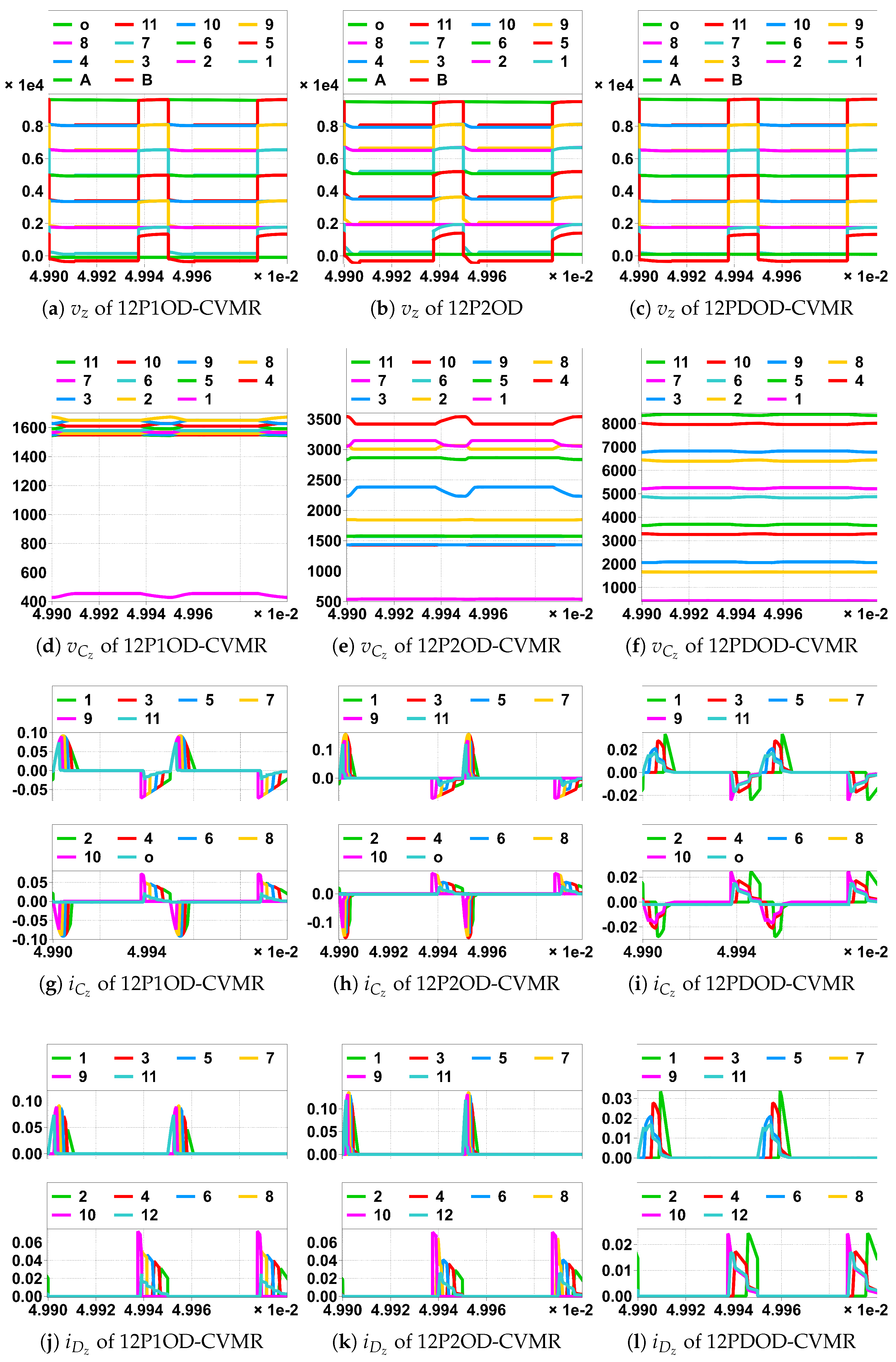
Figure 19.
Simulation of CVMR part of the UHGH converters of Family4; (legend number is the value of z). In horizontal scale ×1e-2 means , unit is Second.
Figure 19.
Simulation of CVMR part of the UHGH converters of Family4; (legend number is the value of z). In horizontal scale ×1e-2 means , unit is Second.
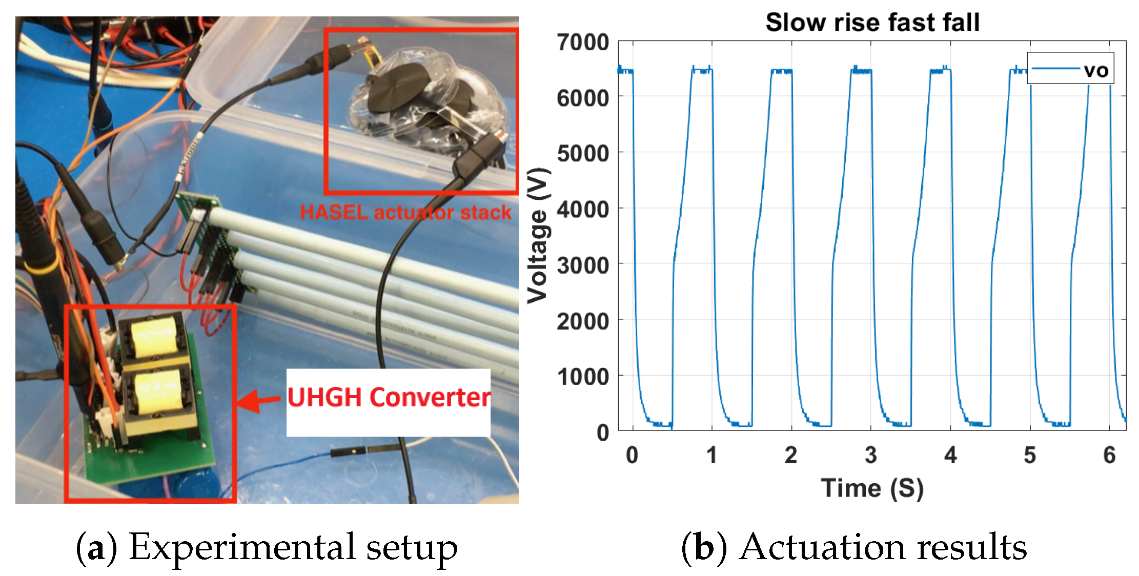
Figure 20.
Demonstration of a UHGH converter with HASEL.
Figure 20.
Demonstration of a UHGH converter with HASEL.
Table 1.
KCL to relate different in 12P(N)OD-CVMR.
Table 1.
KCL to relate different in 12P(N)OD-CVMR.
| | |
|---|
| Curr. Enters | Curr. Enters | Curr. Enters | Curr. Enters | Curr. Enters | Curr. Enters |
|---|
| | | | | | |
| | | | | |
| | | | | |
| | | | | |
| | | | | |
| | | | | |
Table 2.
KVL to relate different .
Table 2.
KVL to relate different .
| | |
|---|
| Curr. Enters | Curr. Enters | Curr. Enters | Curr. Enters | Curr. Enters | Curr. Enters |
|---|
| | | | | |
| | | | | |
| | | | | |
| | | | | |
| | | | | |
| | | | | |
Table 3.
of 12P(N)OD-CVMR obtained through KVL.
Table 3.
of 12P(N)OD-CVMR obtained through KVL.
| N | |
|---|
| 1 | |
| 2 | |
| ∞ | |
Table 4.
, , , and of flying Caps. in 12P1OD-CVMR.
Table 4.
, , , and of flying Caps. in 12P1OD-CVMR.
| Cap. | 12P1OD-CVMR |
|---|
| | | | |
|---|
| 6 | | | |
| 5 | | | |
| 5 | | | |
| 4 | | | |
| 4 | | | |
| 3 | | | |
| 3 | | | |
| 2 | | | |
| 2 | | | |
| 1 | | | |
| 1 | | | |
| 1 | | | |
Table 5.
, , , and of flying Caps. in 12P2OD-CVMR.
Table 5.
, , , and of flying Caps. in 12P2OD-CVMR.
| Cap. | 12P2OD-CVMR |
|---|
| | | | |
|---|
| 1 | | | |
| 1 | | | |
| 5 | | | |
| 4 | | | |
| 1 | | | |
| 1 | | | |
| 3 | | | |
| 2 | | | |
| 1 | | | |
| 1 | | | |
| 1 | | | |
| 1 | | | |
Table 6.
, , , and of flying Caps. in 12PDOD-CVMR.
Table 6.
, , , and of flying Caps. in 12PDOD-CVMR.
| Cap. | 12PDOD-CVMR |
|---|
| | | | |
|---|
| 1 | | | |
| 1 | | | |
| 1 | | | |
| 1 | | | |
| 1 | | | |
| 1 | | | |
| 1 | | | |
| 1 | | | |
| 1 | | | |
| 1 | | | |
| 1 | | | |
| 1 | | | |
Table 7.
Effective capacitance seen at the input node of 12P(N)OD-CVMR.
Table 7.
Effective capacitance seen at the input node of 12P(N)OD-CVMR.
| Figure 2b | | | |
| Figure 2c | | | |
| Figure 3b | | | |
| Figure 3c | | | |
| Figure 4b | | | |
| Figure 4c | | | |
Table 8.
Approximate theoretical analysis of the UHGH converters.
Table 8.
Approximate theoretical analysis of the UHGH converters.
| Conv. | | Avg. Curr. Ind. | Avg. Volt. Cap. | SW. Volt. | HVW Volt. |
|---|
| Family1 |
| Figure 5a | | | NA | | |
| Figure 5b | | | NA | | |
| Family2 |
| Figure 6a | | | | | |
| Figure 6b | | | | | |
| Family3 |
| Figure 7a | | | | | |
| Figure 7b | | | | | |
| Family4 |
| Figure 8a | | | | | |
| Figure 8b | | | | | |
Table 9.
Simulation Results of the HGSME of the UHGH converters.
Table 9.
Simulation Results of the HGSME of the UHGH converters.
| Conv. | Ind. (uH) | Avg. Ind. Curr. (A) | Cap. (uF) | Avg. Cap. Volt. (V) |
|---|
| Family1 |
| Figure 5a | | | NA | NA |
| Figure 5b | | | NA | NA |
| Family2 |
| Figure 6a | | | | |
| Figure 6b | | | | |
| Family3 |
| Figure 7a | | | | |
| Figure 7b | | | | |
| Family4 |
| Figure 8a | | | | |
| Figure 8b | | ; | | ; |
Table 10.
Composition of the circuit.
Table 10.
Composition of the circuit.
| Part Name | Part Number | Rating | PPU ($) | WPU (Oz) |
|---|
| Micro-controller | TMS320f28379D | | 14.56 | 0.09 |
| Half-bridge driver | UCC27201DR | 120 V, 3 A | 0.756 | 0.00256 |
| Low-side driver | IX4427NTR | 34 V, 1.5 A | 0.35 | 0.019 |
| Decoup. Cap. | C0805C105K3RAC7210 | 25 V, 1 uF | 0.22 | 0.0002 |
| Boot-strap capacitor | C0805C104K3RACTU | 25 V, 0.1 uF | 0.037 | 0.0002 |
| C2012X5R1V226M125AC | 35 V, 22 uF | 0.285 | 0.0002 |
| SIRA20DP-T1-RE3 | 25 V, 63 A | 0.56 | 0.018 |
| XF0757-EF25R-A | 1:100 | 1.85 | 1.8 |
| GAP3SLT33-214 | 3.3 kV, 0.3 A | 7.3 | 0.0035 |
| IXTY02N120P | 1.2 kV, 0.2 A | 0.66 | 0.08 |
| GP02-40-E3/73 | 5 kV, 0.25 A | 0.14 | 0.012 |
| HVCC153Y6P202MEAX | 2 nF, 15 kV | 2.17 | 0.237 |
| 2225WC223KAT1A | 22 nF, 2.5 kV | 1.66 | 0.02481 |
| HV2225Y332KXmathV | 3.3 nF, 5 kV | 1.14 | 0.044446 |
| HVCC153Y6P202MEAX | 2 nF, 15 kV | 2.17 | 1.659 |
Table 11.
Comparison with [
33].
Table 11.
Comparison with [
33].
| Conv. Capabilities | [33] | This |
|---|
| Max. Op. Volt. (kV) | 5 | 7 |
| Max. Op. Curr. (mA) | 0.15 | 5 |
| Max. Op. Pow. (W) | 0.75 | 25 |
| Pow. Density (W/in3) | 0.06 | 0.4 |
| Pow. Density (W/g) | 0.0125 | 0.15 |
| Cost (USD) | 390 | 70 |
| Pow. Density (W/$) | 0.002 | 0.36 |
Table 12.
Qualitative comparison of the UHGH converters.
Table 12.
Qualitative comparison of the UHGH converters.
Table 13.
Comparison of output voltages of different HGSMEs and s of different CVMRs of the UHGH converters.
Table 13.
Comparison of output voltages of different HGSMEs and s of different CVMRs of the UHGH converters.
| Conv. | N | | | | | | | | | | | | | | |
|---|
| Families 1 (Figure 5), 2 (Figure 6) and 3 (Figure 7) | ∞ | 0.8 | 0.8 | 0.8 | 1.6 | 2.4 | 3.2 | 4 | 4.8 | 5.6 | 6.4 | 7.2 | 8 | 8.8 | 9.6 |
| 2 | 0.9 | 0.9 | 0.9 | 1.8 | 2.5 | 3.5 | 1.5 | 1.5 | 3 | 3 | 1.4 | 1.4 | 2.7 | 9.3 |
| 1 | 0.9 | 0.9 | 0.9 | 1.7 | 1.6 | 1.6 | 1.6 | 1.6 | 1.6 | 1.6 | 1.6 | 1.6 | 1.6 | 9.6 |
| Family 4 (Figure 8) | ∞ | 0.4 | 1.4 | 0.4 | 1.6 | 2 | 3.2 | 3.6 | 4.8 | 5.2 | 6.4 | 6.8 | 8 | 8.4 | 9.6 |
| 2 | 0.5 | 1.3 | 0.5 | 1.8 | 2.4 | 3.4 | 1.6 | 1.6 | 3.1 | 3 | 1.4 | 1.4 | 2.8 | 9.5 |
| 1 | 0.4 | 1.2 | 0.4 | 1.6 | 1.6 | 1.6 | 1.6 | 1.6 | 1.6 | 1.6 | 1.6 | 1.5 | 1.5 | 9.6 |


