
Electrolytic Recovery of Indium from Copper Indium Gallium Selenide Photovoltaic Panels: Preliminary Investigation of Process Parameters

Abstract
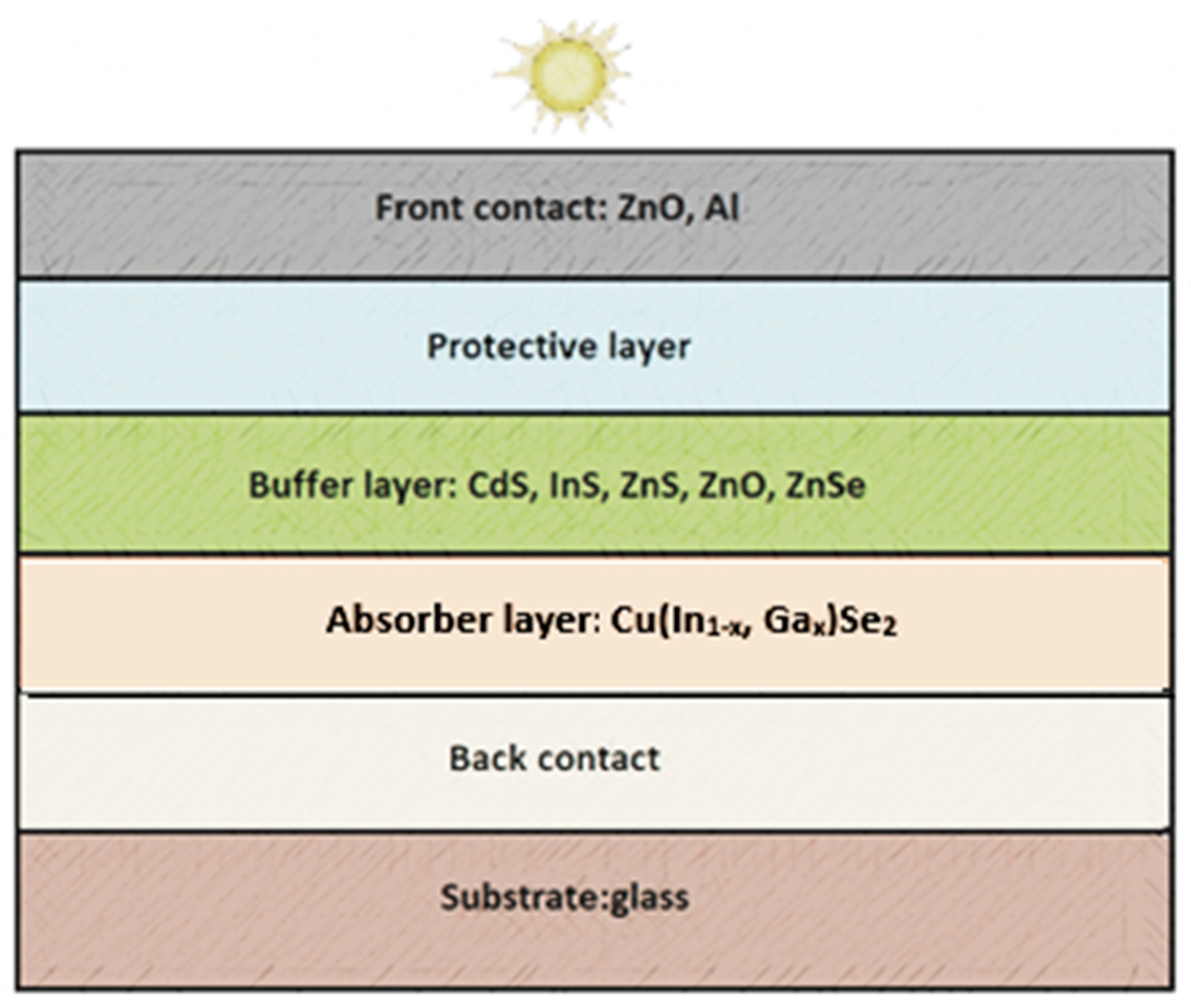
1. Introduction
- 65–75% glass (by weight);
- 10–15% polymer layers (e.g., EVA, back contact);
- 5–10% metals such as aluminum, molybdenum, and copper;
- <2% semiconducting layer, which includes copper, indium, gallium, and selenium;
- Indium content typically ranging from 100 to 300 ppm, depending on thickness and manufacturer specifications.
- -
- Minimizing carrier loss: The buffer layer helps minimize carrier recombination, which can occur at the interface between the absorber layer and the current-collecting layer. Recombination is the process where charge carriers (electrons and holes) combine and lose their energy, which is undesirable as it affects the efficiency of solar energy conversion.
- -
- Improving electrostatic balance: The buffer layer helps maintain electrostatic balance between the absorber layer and the current-collecting layer, which is crucial for effective charge carrier transport.
- -
- Protection of the absorber layer: The buffer layer also serves a protective role, shielding the absorber layer from damage and the effects of atmospheric conditions.
- -
- Improving panel structure coherence: Adding a buffer layer can improve the coherence of panel structures, which is crucial for achieving uniform and efficient solar energy conversion.
2. Materials and Methods
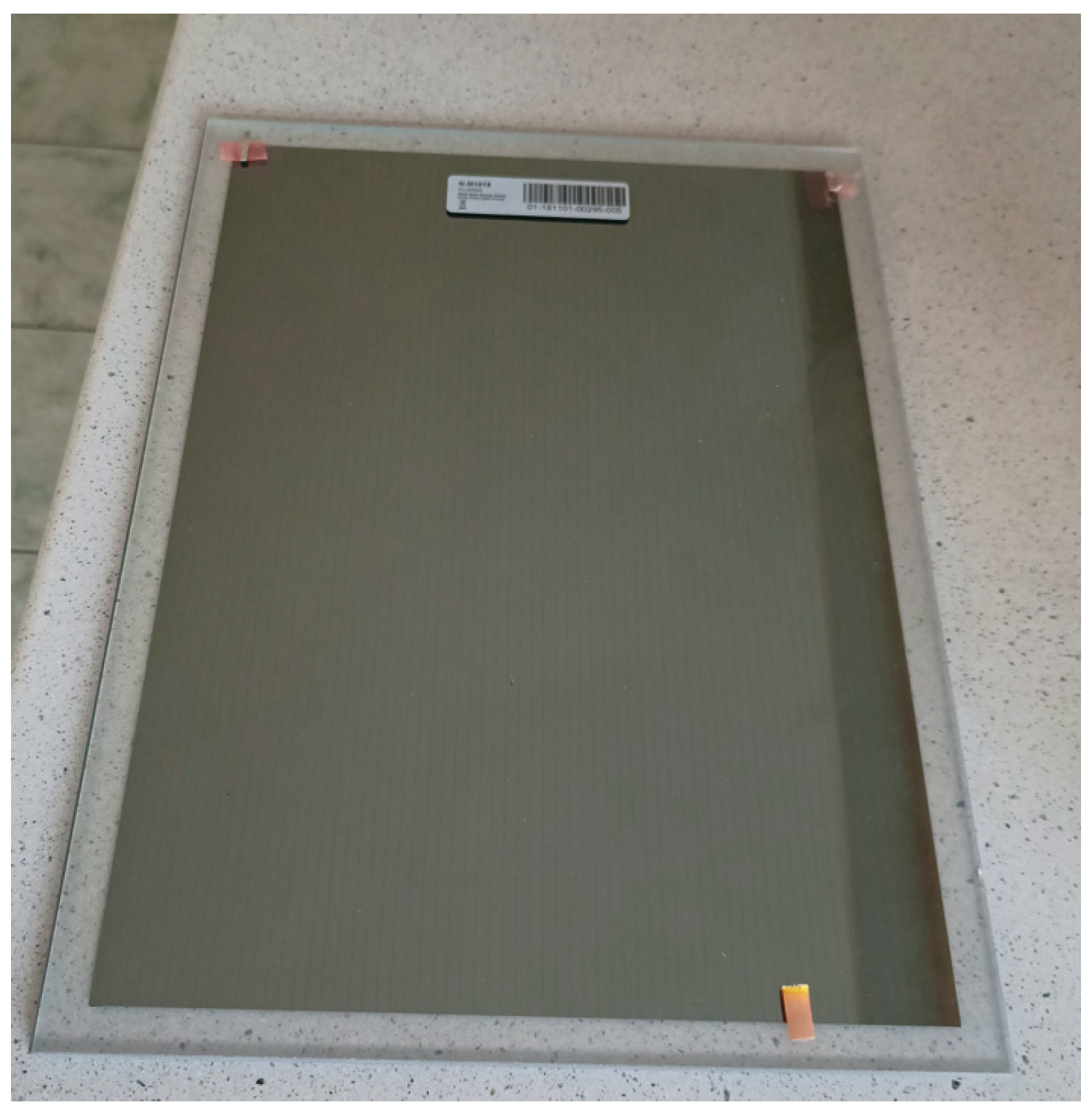
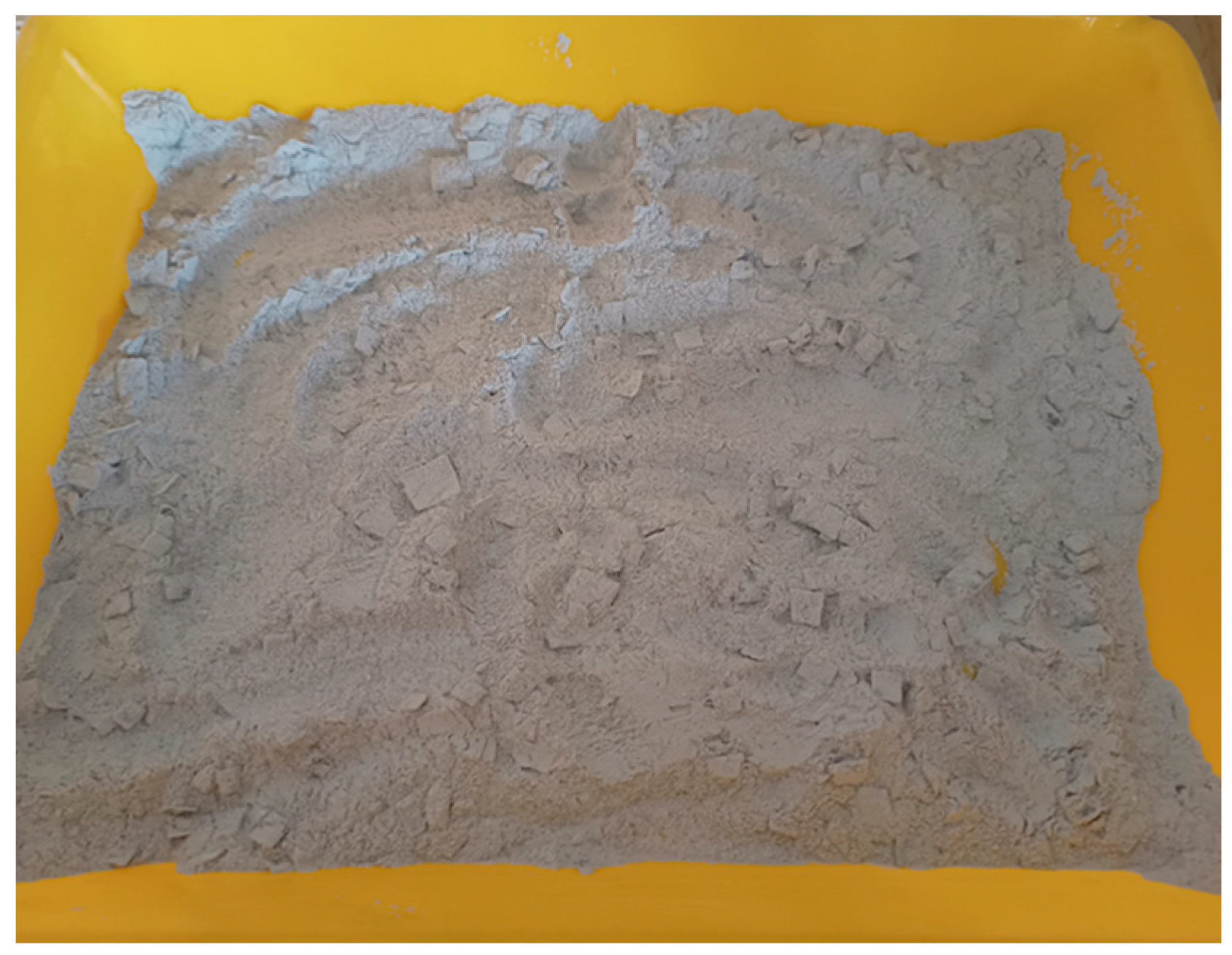
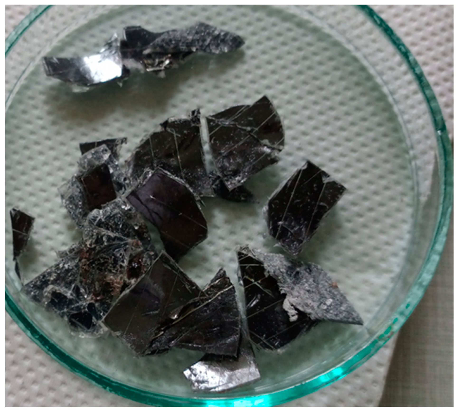
2.1. Preparation of the Photovoltaic Panel for Laboratory Studies
2.2. Inductively Coupled Plasma Mass Spectrometry (ICP-MS)
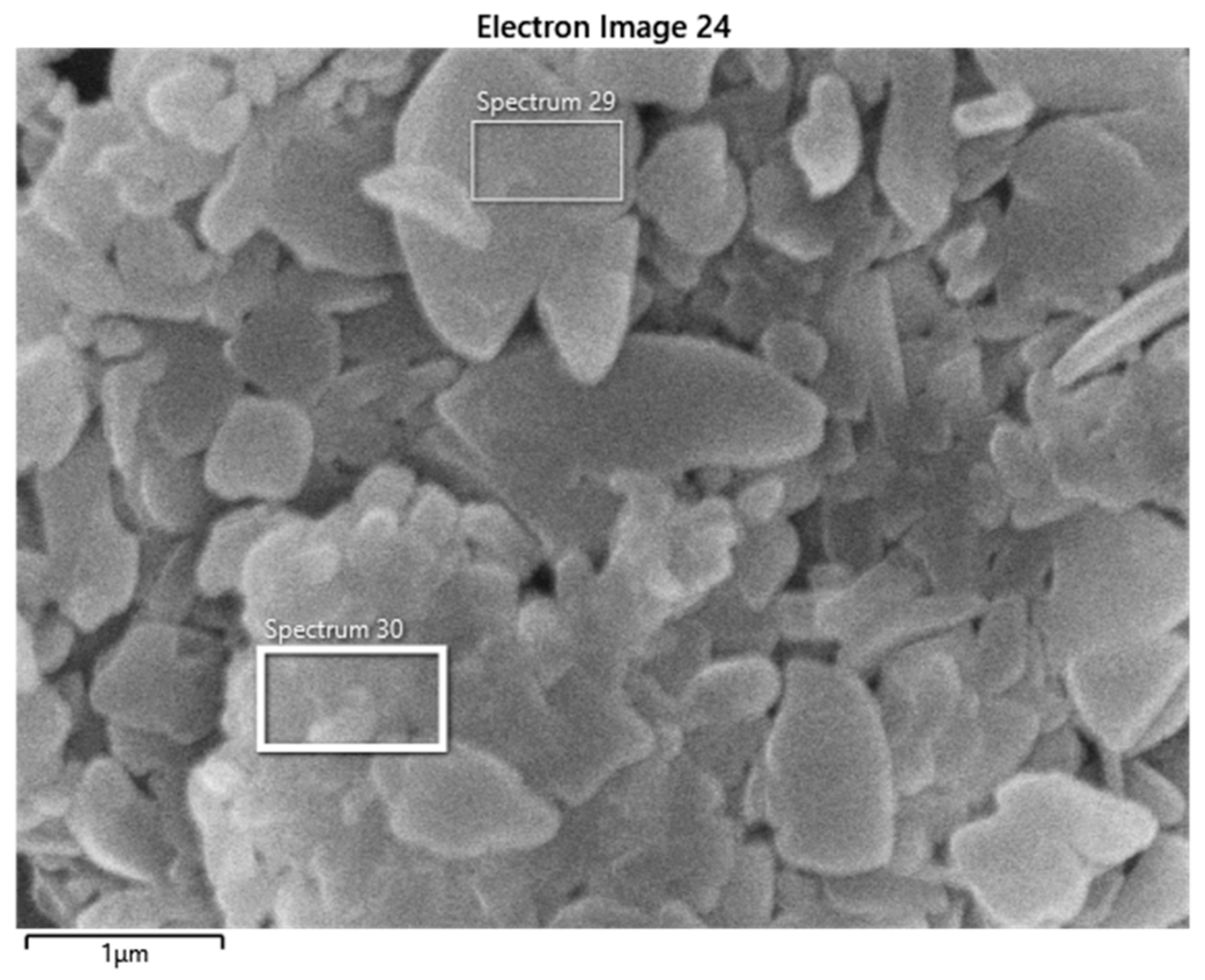
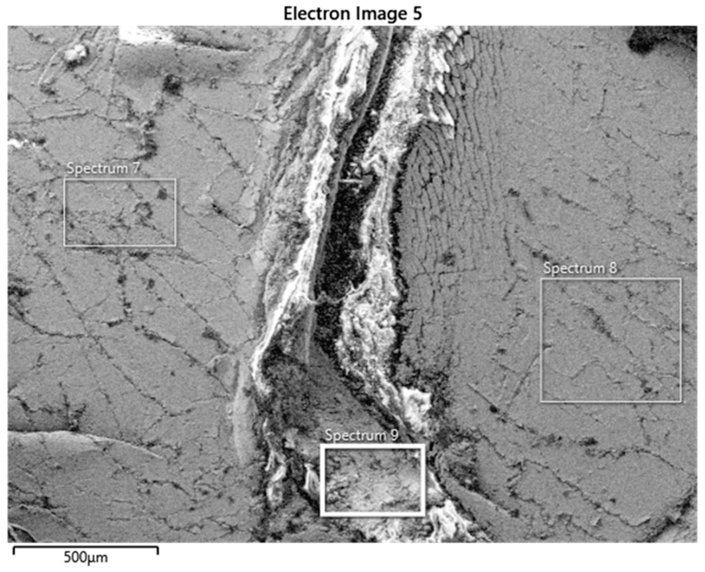
2.3. Scanning Electron Microscopy
- -
- Secondary Electrons (SE) detector used for imaging the surface morphology of materials.
- -
- Backscattered Electrons (BSE) detector utilized for imaging with chemical composition contrast.
- -
- Transmission Electron Detector (TED) employed for observing “thin” samples in transmission mode.
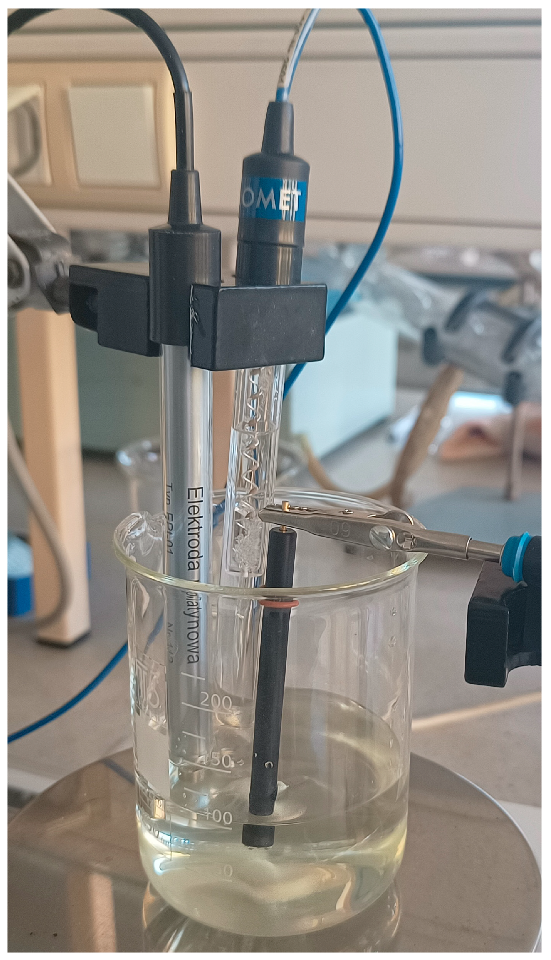
2.4. Electrolysis Operating Conditions
- -
- A chlorosilver electrode type RL-100 was used as a reference electrode. It contains a Ag/AgCl half-panel immersed in a non-exchangeable, potassium chloride solution saturated with silver chloride. The reference half-panel is shielded by an outer chamber filled with an intermediate (protective) solution, which is in contact with the sample under investigation via an external electrolytic connector. A 4.0 M potassium chloride solution is used as the intermediate solution.
- -
- A platinum electrode type EPt-01 served as the counter electrode. Its potential depends on the redox equilibrium in the solution. It cannot be used independently but rather in conjunction with a reference electrode with a potential largely independent of the composition of the solution under study. Both electrodes, when connected to a pH/millivoltmeter, form a redox potential measurement panel. The indicator element of the electrode is a platinum ring permanently attached to the end of the glass body.
- -
- A carbon electrode, specifically the Glassy Carbon Voltammetry Electrode (BASMF2012-1EA, Bioanalytical Systems, Inc. (BASi®), West Lafayette, IN, USA), was used as the working electrode. Its main advantages include temperature resistance, high hardness and durability, a wide potential window, and chemical stability.
- -
- H2O2 (30% concentration, Merck);
- -
- Concentrated HCl (high purity, 35–38%, ROMIL);
- -
- HNO3 (high purity, 67–69%, ROMIL);
- -
- 1 M HCl—prepared in the laboratory by dissolving concentrated HCl in deionized water;
- -
- 3 M HCl—prepared in the laboratory by dissolving concentrated HCl in deionized water;
- -
- 1 M HNO3—prepared in the laboratory by dissolving concentrated HNO3 in deionized water;
- -
- NH4Cl (analytical grade, POCH);
- -
- Indium beads, diam. 2–5 mm, 99.999% trace metals basis, Sigma Aldrich.
- -
- Ultrasonic bath with heating function up to 80 °C, SONOREX Bandelin;
- -
- Muffle furnace with temperature gradient setting capability in the range of 30–1800 °C;
- -
- Magnetic stirrer MS11 WIGO;
- -
- Analytical balance Mettler Toledo XP 205.
3. Results and Discussion
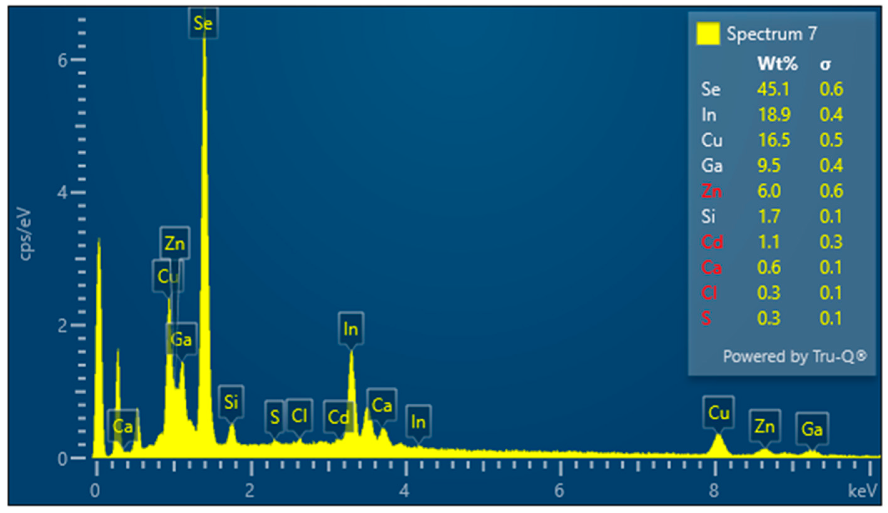
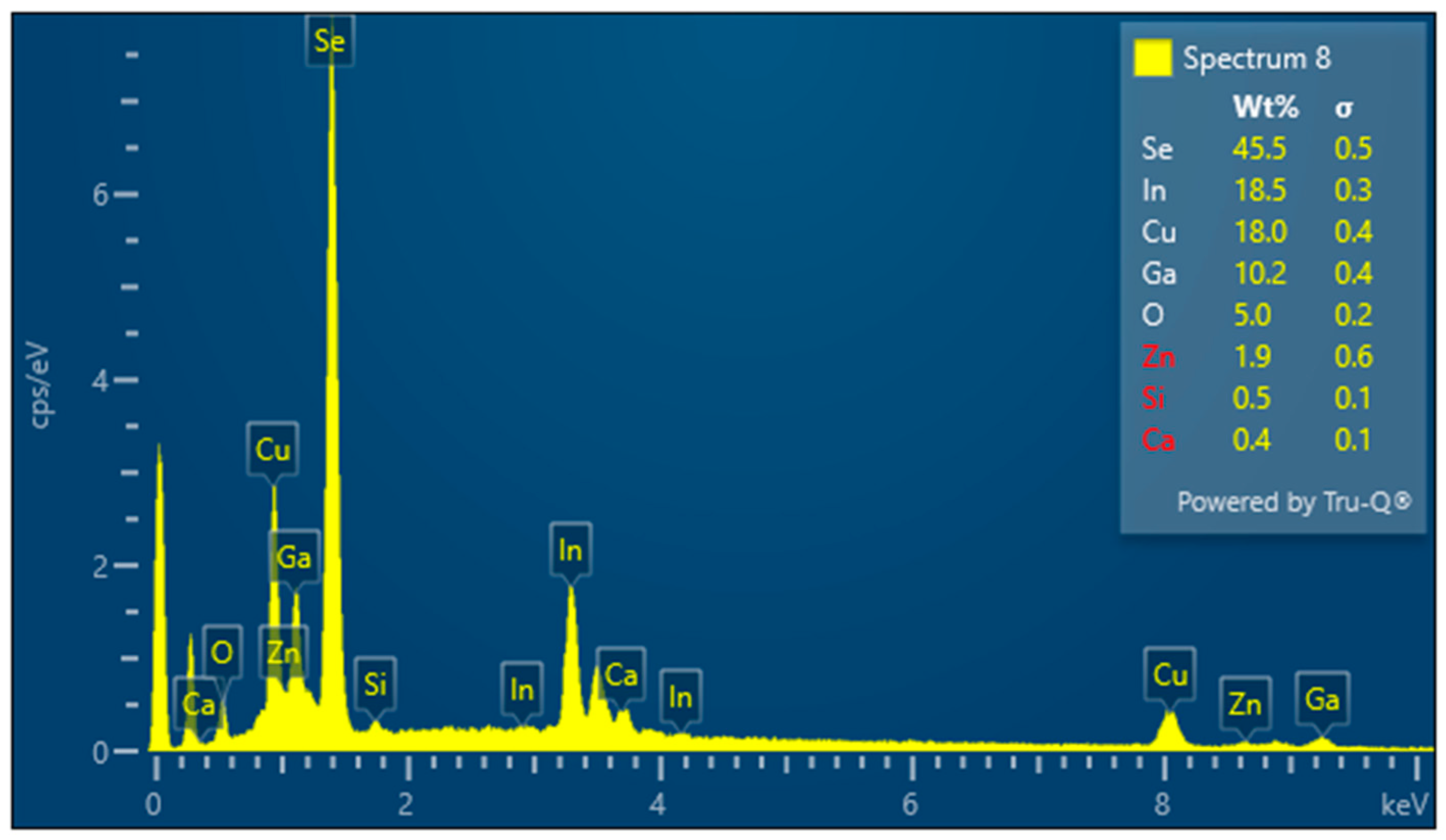
3.1. Indium Content Analysis in Averaged Panel Samples Versus Samples from the Absorbing Layer
3.2. Preparation of Panel Samples for Electrolysis
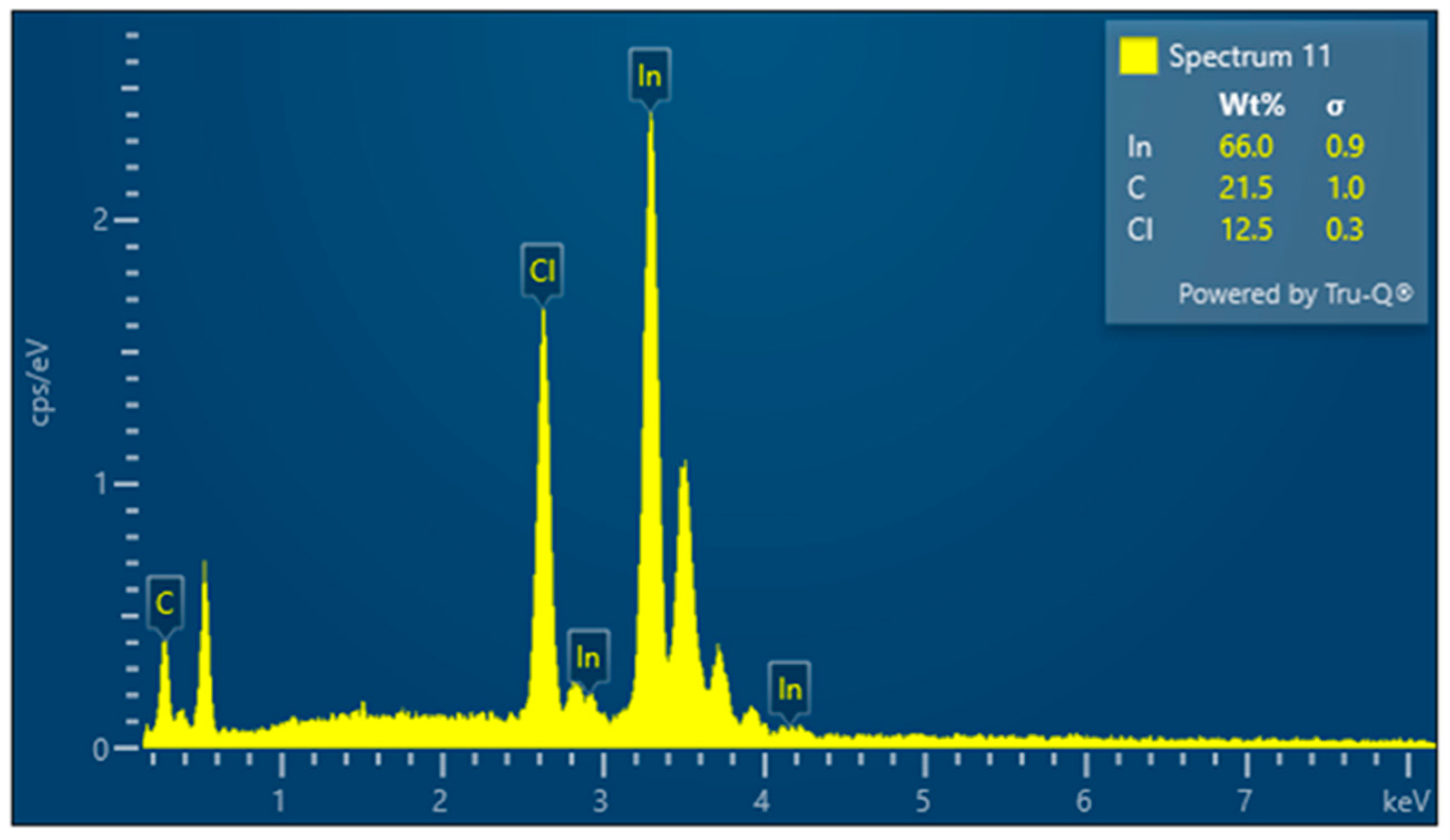
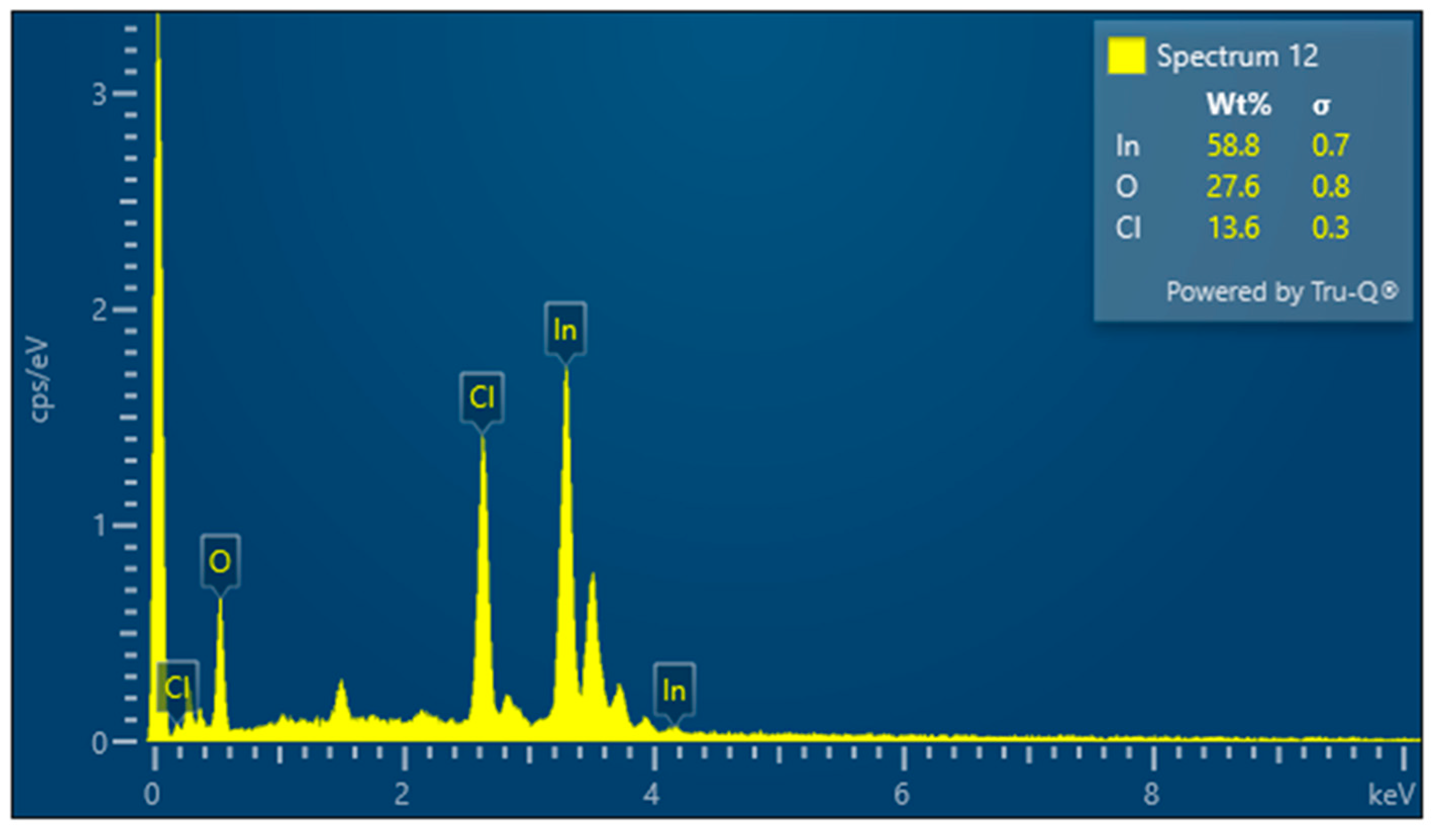
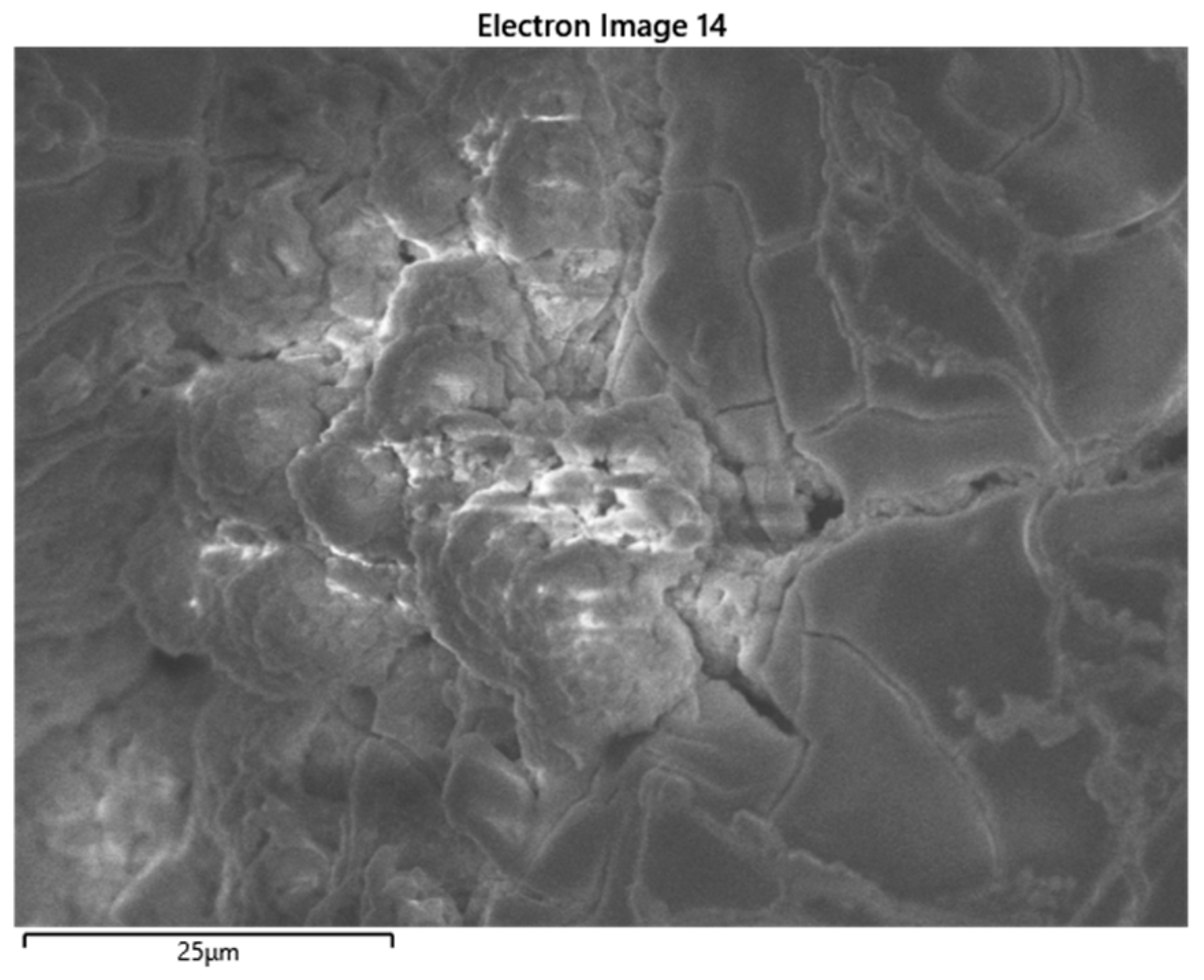
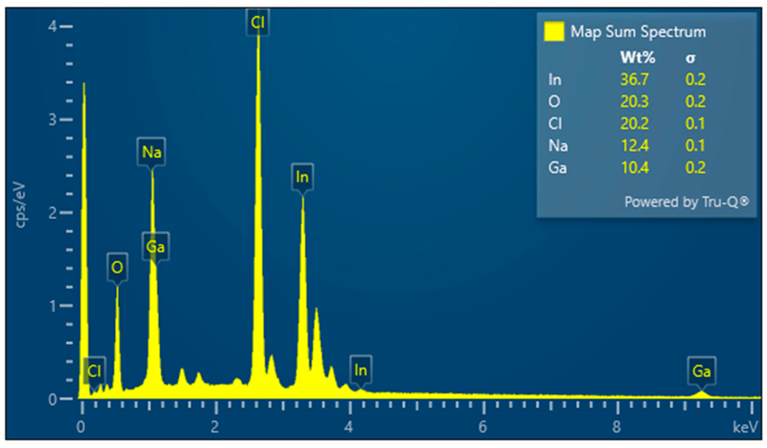
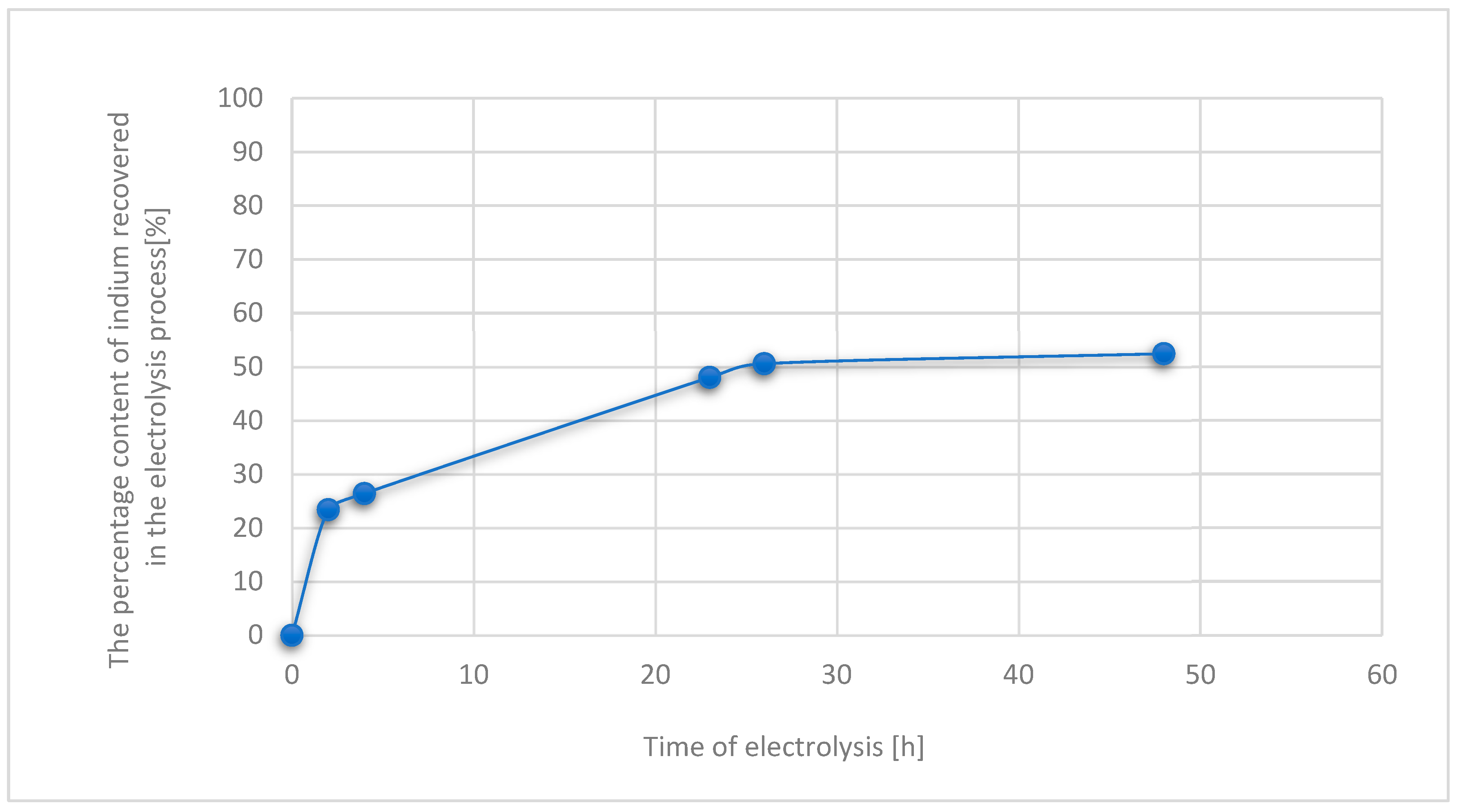
3.3. Results for Samples Deposited on the Electrode
4. Conclusions
Author Contributions
Funding
Data Availability Statement
Conflicts of Interest
Abbreviations
| CIGS | Copper indium gallium selenide panel |
| ICP-MS | Inductively Coupled Plasma Mass Spectrometry |
| SEM | Scanning Electron Microscopy |
| SE | Secondary Electrons detector |
| BSE | Backscattered Electrons detector |
| TED | Transmission Electron Detector |
| LCDs | liquid crystal displays |
| LEDs | light-emitting diodes |
| RF | radio frequency |
References
- Li, X.; Ma, B.; Wang, C.; Hu, D.; Lü, Y.; Chen, Y. Recycling and recovery of spent copper—Indium—Gallium—Diselenide (CIGS) solar cells: A review. Int. J. Min. Met. Mater. 2023, 30, 989–1002. [Google Scholar] [CrossRef]
- Shamim, S.M.; Islam, S.; Huq, M.F.; Al Jobair, M. Design, performance analysis and efficiency optimization of copper indium gallium selenide (CIGS) solar cell. Eur. Sci. J. ESJ. 2015, 11. Available online: https://eujournal.org/index.php/esj/article/view/5133 (accessed on 11 April 2025).
- Kuczyńska-Łażewska, A.; Klugmann-Radziemska, E.; Witkowska, A. Recovery of Valuable Materials and Methods for Their Management When Recycling Thin-Film CdTe Photovoltaic Modules. Materials 2021, 14, 7836. [Google Scholar] [CrossRef] [PubMed] [PubMed Central]
- Isherwood, P. Reshaping the Module: The Path to Comprehensive Photovoltaic Panel Recycling. Sustainability 2022, 14, 1676. [Google Scholar] [CrossRef]
- Petroli, P.A.; Camargo, P.S.S.; de Souza, R.A.; Veit, H.M. Assessment of Toxicity Tests for Photovoltaic Panels: A Review. Curr. Opin. Green Sustain. Chem. 2024, 47, 100885. [Google Scholar] [CrossRef]
- PW Consulting. CIGS Solar Panels Market; PW Consulting Chemical & Energy Research Center: 9 February 2025. Available online: https://pmarketresearch.com/chemi/cigs-solar-panels-market/ (accessed on 11 April 2025).
- European Commission. Critical Raw Materials Resilience: Charting a Path Towards Greater Security and Sustainability; COM(2023) 221 final; European Commission: Brussels, Belgium, 2023. Available online: https://ec.europa.eu/info/publications/critical-raw-materials-resilience-charting-path-towards-greater-security-and-sustainability_en (accessed on 11 April 2025).
- Amato, A.; Beolchini, F. End-of-Life CIGS Photovoltaic Panel: A Source of Secondary Indium and Gallium. Prog. Photovolt. Res. Appl. 2018, 27, 229–236. [Google Scholar] [CrossRef]
- Philipps, S.; Warmuth, W. Photovoltaics Report; Fraunhofer ISE and PSE Projects GmbH: Last Updated: 29 July 2024. Available online: https://www.ise.fraunhofer.de/en/publications/studies/photovoltaics-report.html (accessed on 9 April 2025).
- Zhao, C.; Yu, S.; Tang, W.; Yuan, X.; Zhou, H.; Qi, T.; Zheng, X.; Ning, D.; Ma, M.; Zhu, J.; et al. Advances in CIGS Thin Film Solar Cells with Emphasis on the Alkali Element Post-Deposition Treatment. Mater. Rep. Energy 2023, 3, 100214. [Google Scholar] [CrossRef]
- Theocharis, M.; Tsakiridis, P.E.; Kousi, P.; Hatzikioseyian, A.; Zarkadas, I.; Remoundaki, E.; Lyberatos, G. Hydrometallurgical Treatment for the Extraction and Separation of Indium and Gallium from End-of-Life CIGS Photovoltaic Panels. Mater. Proc. 2021, 5, 51. [Google Scholar] [CrossRef]
- Rocchetti, L.; Beolchini, F. Recovery of Valuable Materials from End-of-Life Thin-Film Photovoltaic Panels: Environmental Impact Assessment of Different Management Options. J. Clean. Prod. 2015, 89, 59–64. [Google Scholar] [CrossRef]
- Li, M.; Widijatmoko, S.D.; Wang, Z.; Hall, P. A Methodology to Liberate Critical Metals in Waste Solar Panel. Appl. Energy 2023, 337, 120900. [Google Scholar] [CrossRef]
- Li, X.; Ma, B.; Hu, D.; Zhao, Q.; Chen, Y.; Wang, C. Efficient Separation and Purification of Indium and Gallium in Spent Copper Indium Gallium Diselenide (CIGS). J. Clean. Prod. 2022, 339, 130658. [Google Scholar] [CrossRef]
- White, S.J.O.; Shine, J.P. Exposure Potential and Health Impacts of Indium and Gallium, Metals Critical to Emerging Electronics and Energy Technologies. Curr. Environ. Health Rep. 2016, 3, 459–467. [Google Scholar] [CrossRef]
- Mufti, N.; Amrillah, T.; Taufiq, A.; Sunaryono; Aripriharta; Diantoro, M.; Zulhadjri; Nur, H. Review of CIGS-Based Solar Cells Manufacturing by Structural Engineering. Sol. Energy 2020, 207, 1146–1157. [Google Scholar] [CrossRef]
- Moradi, M.; Teimouri, R.; Saadat, M.; Zahedifar, M. Buffer layer replacement: A method for increasing the conversion efficiency of CIGS thin film solar panels. Optik 2017, 136, 222–227. [Google Scholar] [CrossRef]
- Fthenakis, V. Sustainability of Photovoltaics: The Case for Thin-Film Solar Cells. Renew. Sustain. Energy Rev. 2009, 13, 2746–2750. [Google Scholar] [CrossRef]
- Wang, J.; Feng, Y.; He, Y. Advancements in Recycling Technologies for Waste CIGS Photovoltaic Modules. Nano Energy 2024, 128, 109847. [Google Scholar] [CrossRef]
- Available online: https://tradingeconomics.com/commodity/ (accessed on 11 April 2025).
- Gustafsson, A.M.K. Recycling of CIGS Solar Cell Waste Materials. Ph.D. Thesis, Chalmers University of Technology, Gothenburg, Sweden, 2014. Available online: https://publications.lib.chalmers.se/records/fulltext/203661/203661.pdf (accessed on 11 April 2025).
- Pang, S.; Yan, Y.; Wang, Z.; Wang, D.; Li, S.; Wei, K. Enhanced Separation of Different Layers in Photovoltaic Panel by Mi-crowave Field. Sol. Energy Mater. Sol. Cells 2021, 230, 111213. [Google Scholar] [CrossRef]
- Gustafsson, A.M.; Björefors, F.; Steenari, B.M.; Ekberg, C. Investigation of an Electrochemical Method for Separation of Copper, Indium, and Gallium from Pretreated CIGS Solar Cell Waste Materials. Sci. World J. 2015, 2015, 494015. [Google Scholar] [CrossRef] [PubMed] [PubMed Central]
- Gu, S.; Fu, B.T.; Dodbiba, G.; Fujita, T.; Fang, B.Z. Promising approach for recycling of spent CIGS targets by combining electrochemical techniques with dehydration and distillation, ACS Sustain. Chem. Eng. 2018, 6, 6950. [Google Scholar]
- Liu, F.-W.; Cheng, T.-M.; Chen, Y.-J.; Yueh, K.-C.; Tang, S.-Y.; Wang, K.; Wu, C.-L.; Tsai, H.-S.; Yu, Y.-J.; Lai, C.-H.; et al. High-yield recycling and recovery of copper, indium, and gallium from waste copper indium gallium selenide thin-film solar panels. Sol. Energy Mater. Sol. Cells 2022, 241, 111691. [Google Scholar] [CrossRef]
- Teknetzi, I.; Holgersson, S.; Ebin, B. Valuable metal recycling from thin film CIGS solar cells by leaching under mild conditions. Sol. Energy Mater. Sol. Cells 2023, 252, 112178. [Google Scholar] [CrossRef]
- Hu, D.; Ma, B.; Li, X.; Lv, Y.; Zhang, W.; Chen, Y.; Wang, C. Efficient separation and recovery of gallium and indium in spent CIGS materials. Sep. Purif. Technol. 2022, 282, 120087. [Google Scholar] [CrossRef]
- Marchetti, B.; Corvaro, F.; Giacchetta, G.; Polonara, F.; Cocci Grifoni, R.; Leporini, M. Double Green Process: A Low Environmental Impact Method for Recycling of CdTe, a-Si, and CIS/CIGS Thin-Film Photovoltaic Modules. Int. J. Sustain. Eng. 2018, 11, 173–185. [Google Scholar] [CrossRef]
- Teknetzi, I.; Click, N.; Holgersson, S.; Ebin, B. An Environmentally Friendly Method for Selective Recovery of Silver and ITO Particles from Flexible CIGS Solar Cells. Sustain. Mater. Technol. 2024, 39, e00844. [Google Scholar] [CrossRef]
- Padoan, F.C.S.M.; Altimari, P.; Pagnanelli, F. Recycling of End-of-Life Photovoltaic Panels: A Chemical Prospective on Process Development. Sol. Energy 2019, 177, 746–761. [Google Scholar] [CrossRef]
- Bae, D. A Statistical Approach to Scaling Up of CIGS PV Cells: Quantitative Analysis of Composition Uniformity within and between the Samples. Mater. Sci. Semicond. Process. 2023, 164, 107626. [Google Scholar] [CrossRef]
- Bulińska, S.; Sujak, A.; Pyzalski, M. Sustainable Management of Photovoltaic Waste Through Recycling and Material Use in the Construction Industry. Materials 2025, 18, 284. [Google Scholar] [CrossRef]
- Gerold, E.; Antrekowitsch, H. Advancements and Challenges in Photovoltaic Cell Recycling: A Comprehensive Review. Sustainability 2024, 16, 2542. [Google Scholar] [CrossRef]


| Potential [V] | Stirring Speed | Experiment Duration |
|---|---|---|
| −0.902 | 500 rpm | 12–72 h, dependent on the concentration of In in the solution |
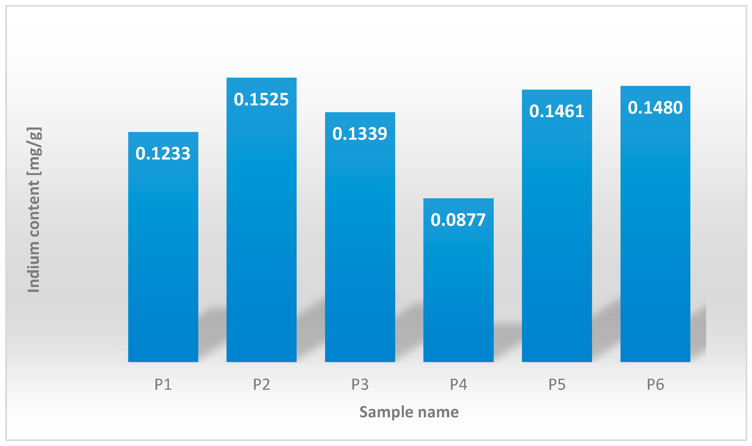
| The Sample Designation | Indium [mg/g CIGS Panel] |
|---|---|
| P1 | 0.1233 |
| P2 | 0.1525 |
| P3 | 0.1339 |
| P4 | 0.0877 |
| P5 | 0.1461 |
| P6 | 0.1480 |
| The minimum value | 0.0877 |
| The maximum value | 0.1525 |
| The median | 0.1400 |
| The arithmetic mean | 0.1319 |
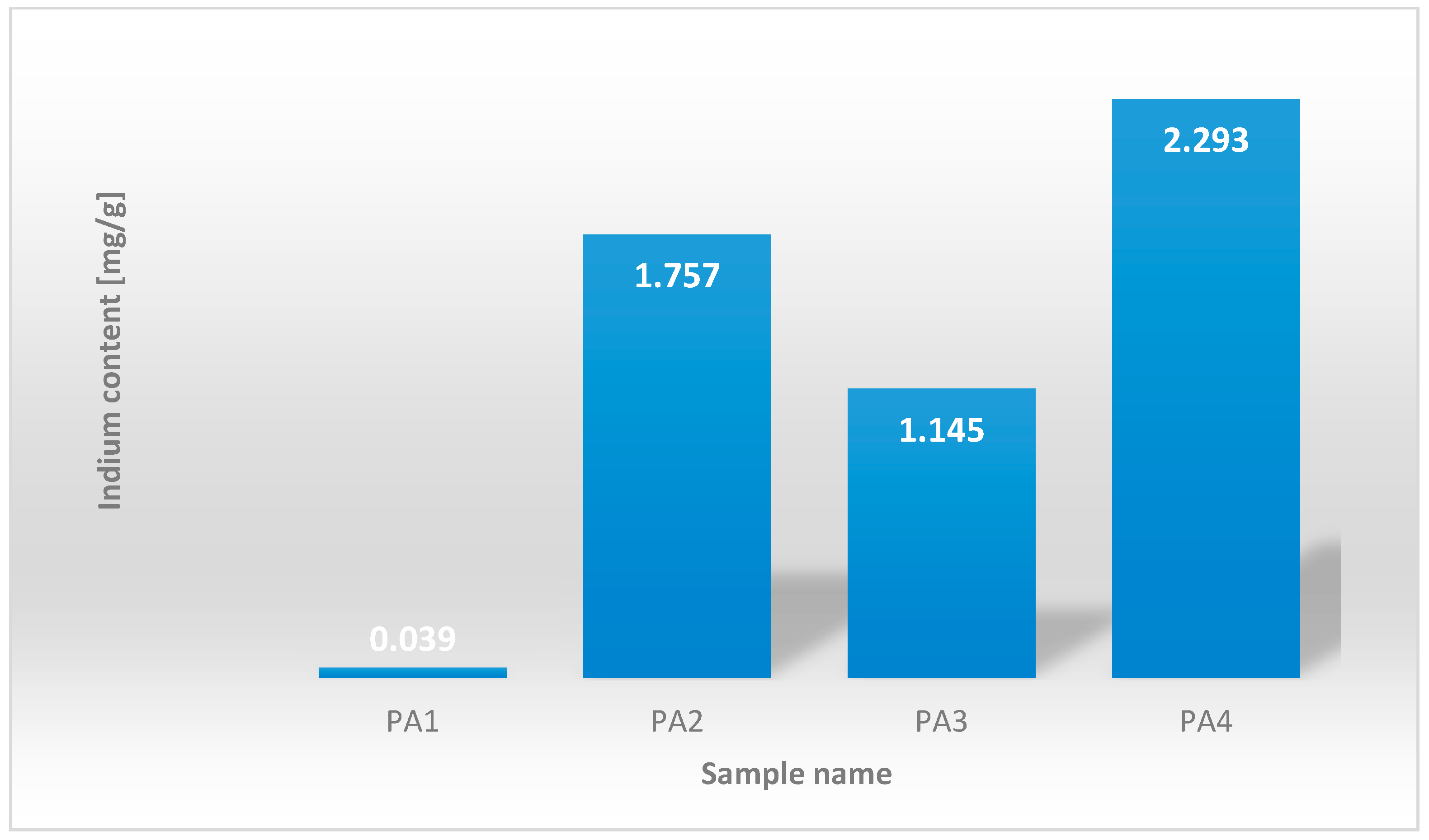
| The Sample Designation | Indium [mg/g of CIGS Panel] |
|---|---|
| PA1 | 0.039 |
| PA2 | 1.757 |
| PA3 | 1.145 |
| PA4 | 2.293 |
| The minimum value | 0.039 |
| The maximum value | 2.293 |
| The median | 1.451 |
| The arithmetic mean | 1.309 |
| Solution Symbol | Preparation of the Solutions |
|---|---|
| R1 | 15 g of CIGS panel sample 460 mL of 3 M HCl 4 × 10 mL of H2O2 Mixed in an ultrasonic bath at 80 °C Washing time: 4 h The eluate was transferred to a 500 mL flask |
| R2 | 15 g of CIGS panel sample 1 g of indium 460 mL of 3 M HCl 4 × 10 mL of H2O2 Mixed in an ultrasonic bath at 80 °C Washing time: 4 h The eluate was transferred to a 500 mL flask |
Disclaimer/Publisher’s Note: The statements, opinions and data contained in all publications are solely those of the individual author(s) and contributor(s) and not of MDPI and/or the editor(s). MDPI and/or the editor(s) disclaim responsibility for any injury to people or property resulting from any ideas, methods, instructions or products referred to in the content. |
© 2025 by the authors. Licensee MDPI, Basel, Switzerland. This article is an open access article distributed under the terms and conditions of the Creative Commons Attribution (CC BY) license (https://creativecommons.org/licenses/by/4.0/).
Share and Cite
Gajec, M.; Król, A.; Holewa-Rataj, J.; Kukulska-Zając, E.; Kuchta, T. Electrolytic Recovery of Indium from Copper Indium Gallium Selenide Photovoltaic Panels: Preliminary Investigation of Process Parameters. Recycling 2025, 10, 86. https://doi.org/10.3390/recycling10030086
Gajec M, Król A, Holewa-Rataj J, Kukulska-Zając E, Kuchta T. Electrolytic Recovery of Indium from Copper Indium Gallium Selenide Photovoltaic Panels: Preliminary Investigation of Process Parameters. Recycling. 2025; 10(3):86. https://doi.org/10.3390/recycling10030086
Chicago/Turabian StyleGajec, Monika, Anna Król, Jadwiga Holewa-Rataj, Ewa Kukulska-Zając, and Tomasz Kuchta. 2025. "Electrolytic Recovery of Indium from Copper Indium Gallium Selenide Photovoltaic Panels: Preliminary Investigation of Process Parameters" Recycling 10, no. 3: 86. https://doi.org/10.3390/recycling10030086
APA StyleGajec, M., Król, A., Holewa-Rataj, J., Kukulska-Zając, E., & Kuchta, T. (2025). Electrolytic Recovery of Indium from Copper Indium Gallium Selenide Photovoltaic Panels: Preliminary Investigation of Process Parameters. Recycling, 10(3), 86. https://doi.org/10.3390/recycling10030086