Article

Effect of Solvent Pre-Treatment on the Leaching of Copper During Printed Circuit Board Recycling

by
Ahmed Tarek Ismail Mohamed
1,
Giuliana Schimperna
2,
Gianluca Cantoni
2,
Francesca Demichelis
3,
Debora Fino
3,
Sara Perucchini
2,
Francesca Rubertelli
2 and
Francesco Laviano
3,4,*
1
Department of Energy, Politecnico di Torino, 10129 Turin, Italy
2
Eni SpA—Renewable, New Energies and Material Science Research Center, 28100 Novara, Italy
3
Department of Applied Science and Technology, Politecnico di Torino, 10129 Turin, Italy
4
INFN—Sez. Torino, 10125 Torino, Italy
*
Author to whom correspondence should be addressed.
Recycling 2025, 10(3), 80; https://doi.org/10.3390/recycling10030080
Submission received: 28 February 2025 / Revised: 15 April 2025 / Accepted: 22 April 2025 / Published: 1 May 2025

Abstract

:
Printed circuit boards (PCBs) are fundamental components of electronic devices, acting as an important source of various valuable metals such as copper, gold, and silver. Efficient recycling methods that offer high recovery rates are essential to the full reutilization of these materials. Hydrometallurgical leaching is a prominent technique for metal recovery, but its efficiency can be significantly enhanced through solvent pre-treatment. In this study, an experimental analysis of the material composition of different categories of PCBs is presented. In addition, the study evaluates the influence of particle size on the subsequent copper leaching process and the efficiency of copper recovery. These investigations aim to better understand the material composition of PCBs and propose an optimized material recovery technique. The study finds that there are significant variances among the different categories of PCBs investigated, allowing a more informed handling process of WEEE. This research suggests that solvent pretreatment using DMSO for PCB particle sizes between 5.6 mm and 2 mm would be a good optimization technique, mitigating the drawbacks of treating fine particles while maintaining appealing recovery efficiency.

1. Introduction

Printed circuit boards (PCBs) lie at the heart of modern electronic devices, working as connecting paths between electronic components and as a skeletal support. Estimates of the economic value of materials found in Waste Electrical and Electronic Equipment (WEEE) are almost €48 billion, with PCBs containing 40% of these materials [1]. Found in every electronic device, a PCB is a multilayer substrate with copper layers in addition to solder masks and silkscreens. Fiberglass-reinforced epoxy resin (FR4) is typically used for the fabrication of the substrate, offering mechanical strength and insulation. Moreover, phenolic resin and polyimide are also used depending on the application’s requirements [2,3]. The traces, which are the conductive pathways, are made of copper due to its high conductivity.
A high-efficiency material recovery process is crucial from both an economic perspective and a legislative one, especially in the EU, where many of the materials found within WEEE are on the list of critical raw materials, which recently added copper and nickel among them [4,5,6].
The complex composition of PCBs, combining metals, resins, and other materials, makes the recycling process complicated. To mitigate the effect of this complex composition, PCBs are usually size-reduced (typically by shredding or milling) to enable higher-efficiency metal extraction [7]. The efficiency of the subsequent treatment processes is highly dependent on the particle size after size reduction [4,5,6,7].
One of the most common treatment methods for waste PCBs is hydrometallurgical leaching [8], a process that dissolves metals from solid matrices using aqueous solutions to recover them. This method allows high selectivity to extract valuable metals from complex mixtures, making it highly suitable for recycling PCBs with their complex structures. To perform the leaching process, first, the waste PCBs are crushed and ground to reduce their size, increasing the exposed surface area available for chemical reactions during leaching [2]. Acids, alkalis, and complexing agents are then used for the chemical attack. Common leaching agents used for copper recovery processes are sulfuric acid, nitric acid, and ammonia [9,10,11]. The efficiency of the extraction process depends, among other factors, on the temperature, pH, and concentration of the leaching agent, as well as the agitation [12,13,14].
A recent approach to improving the efficiency of hydrometallurgical treatment is adding a chemical pretreatment phase using a solvent after the mechanical reduction of the size of the waste PCBs [15]. The process aims to swell or decompose the resin matrix in PCBs, depending on the organic solvent used, exposing the embedded metal layers, which increases the surface area of metals, consequently improving the efficiency of the leaching process [16]. Moreover, solvent pretreatment was reported as a method for the debromination of plastics found in waste PCBs, as well as other WEEE types [17,18,19,20,21].
Numerous studies have investigated the use of different organic solvents for PCB pretreatment, including but not limited to the use of N-methyl-2-pyrrolidone (NMP) [22], Dimethylformamide (DMF) [23], dimethylacetamide (DMA) [24], and dimethyl sulfoxide (DMSO) [20]. These studies evaluate the factors affecting the efficiency of the pretreatment process, such as the operating temperature, duration of exposure, solvent concentration, and treated particle size. The different pretreatment methods, as well as the optimized conditions for each method, are summarized in Table 1.
DMSO has demonstrated the effective delamination of PCB fragments under specific conditions, such as controlled temperatures (60–170 °C) and solid-to-liquid ratios, with optimal results achieved for smaller particle sizes [22,25,26]. However, in all attempts, the experiments were conducted on relatively large particle sizes rather than powdered PCBs. Furthermore, DMSO presents significant health risks due to its ability to penetrate the skin and the toxicity of its vapors [23].
DMA and DMF have shown promise in treating larger PCB fragments, avoiding the fine crushing process that often leads to metal loss in smaller fractions [24,27]. However, another challenge faced when handling such large pieces of PCBs is the presence of through holes and pins on the PCB, which hinder the swelling process. DMF stands out for its low health risks, ease of regeneration, and compatibility with brominated resins, making it a safer alternative to some solvents [23].
NMP is a strong solvent for PCB treatment, achieving effective resin removal in comparative studies; however, its carcinogenic and reproductive health risks pose significant drawbacks [22,23].
Other techniques also include the use of supercritical fluids, which are considered more eco-friendly and have been effective in removing the organic materials from crushed RAM PCBs at around 300 °C [28,29,30,31]. However, the stability of brominated epoxy resins above 250 °C remains a concern due to potential pollutant emissions [23].
In addition to environmental and efficiency considerations, several patents have proposed innovative approaches, such as multistage treatment processes involving combinations of oxidizing agents, leaching agents, and organic solvents [32,33,34,35].
The advantages of using different pretreatment techniques are the optimization of recovery rates and the mitigation of the challenges posed by varying PCB compositions. In addition, solvent pretreatment reduces the energy used during the treatment process by eliminating the need for extensive mechanical pretreatment, as well as favoring the environmental aspect of the PCB waste handling process.
A more profound inspection of the reported studies shows the lack of information on the effect of solvent pretreatment on the leaching process at fine particle sizes in the micron grade. Such understanding of the impact of solvent pretreatment on small particle sizes is important since most studies on the hydrometallurgical treatment of PCBs had favorable results at particle sizes in micron grade [8,36,37,38,39]. However, PCB treatment using fine particles comes with dust-generation hazards and particle loss [27].
Another gap was also highlighted by [40], which reported that studies focus mainly on the analysis of the dissolved brominated epoxy resin and the regeneration techniques and seldom investigate the effects of swelling on metal leaching and the change in the properties of the treated PCB.
Moreover, an in-depth understanding of PCBs and their material composition is essential for an informed approach to PCB treatment. One recent study investigated the PCB extracted from computers, laptops, and TVs and compared their material content [41]. Furthermore, they compared the different particle size groups and the prevalence of the materials within these groups based on their liberation after grinding, allowing for targeted material recovery with higher efficiency. As a result, they reported that general metals such as copper, zinc, and aluminum are found in coarse fractions between 0.18 and 0.25 mm, while precious metals and rare earth metals (REM) are present in finer sizes. The results complement those from another study, which also studied the metal content of PCBs from computers, laptops, mobile phones, and TVs [42]. It also investigated the best-performing digestion methods for sample preparation and analysis, concluding that the use of strong acids such as hydrogen fluoride (HF) specified in the USEPA 3052 method ensures the effective dissolution of metals embedded within a silica matrix, as in the case of PCBs. These studies, although insightful, leave a gap regarding our knowledge of the material variation among the PCBs extracted from the same WEEE type, such as personal computers.
Based on the identified gaps in the literature, this study aims to investigate the effect of solvent pretreatment on the efficiency of the subsequent leaching process, evaluating how particle size influences recovery rates to optimize the process conditions. Additionally, the study seeks to address the critical question of material variation across different categories and models of PCBs, offering new insights into a largely underexplored area. The research follows an experimental approach to investigate the research questions and evaluate the optimized particle size for solvent pretreatment on a lab scale.
The novelty of this research lies in exploring the swelling of intermediate particle sizes during the solvent pretreatment of motherboard PCBs using DMSO to optimize the conditions, thus mitigating the risks of handling finer particles as well as increasing the copper recovery efficiency to exceed that reached when treating larger particle sizes. Another contribution of this research is that the information obtained from the analysis of the material composition of the different categories of PCBs would allow a more informed decision on whether the separation of PCBs when treating them is justifiable or whether the material variation among the different categories and models is insignificant. The data can also be used to promote more precise calculations in the case of being inserted in calculation models. These areas of novelty fulfill the study objectives to develop an in-depth understanding of PCBs of different categories and find the optimized treatment conditions using the solvent pretreatment method.
The subsequent section reports the results obtained from the analysis of the samples and outlines important relations and comparisons among the different samples analyzed and treated. In Section 3, the paper discusses the materials analyzed and the preparation of the samples for both the analytical analysis of the component material, as well as the investigation of the effect of solvent pretreatment on the selected particle sizes. Finally, Section 4 concludes the key outcomes of this study.

2. Results and Discussion

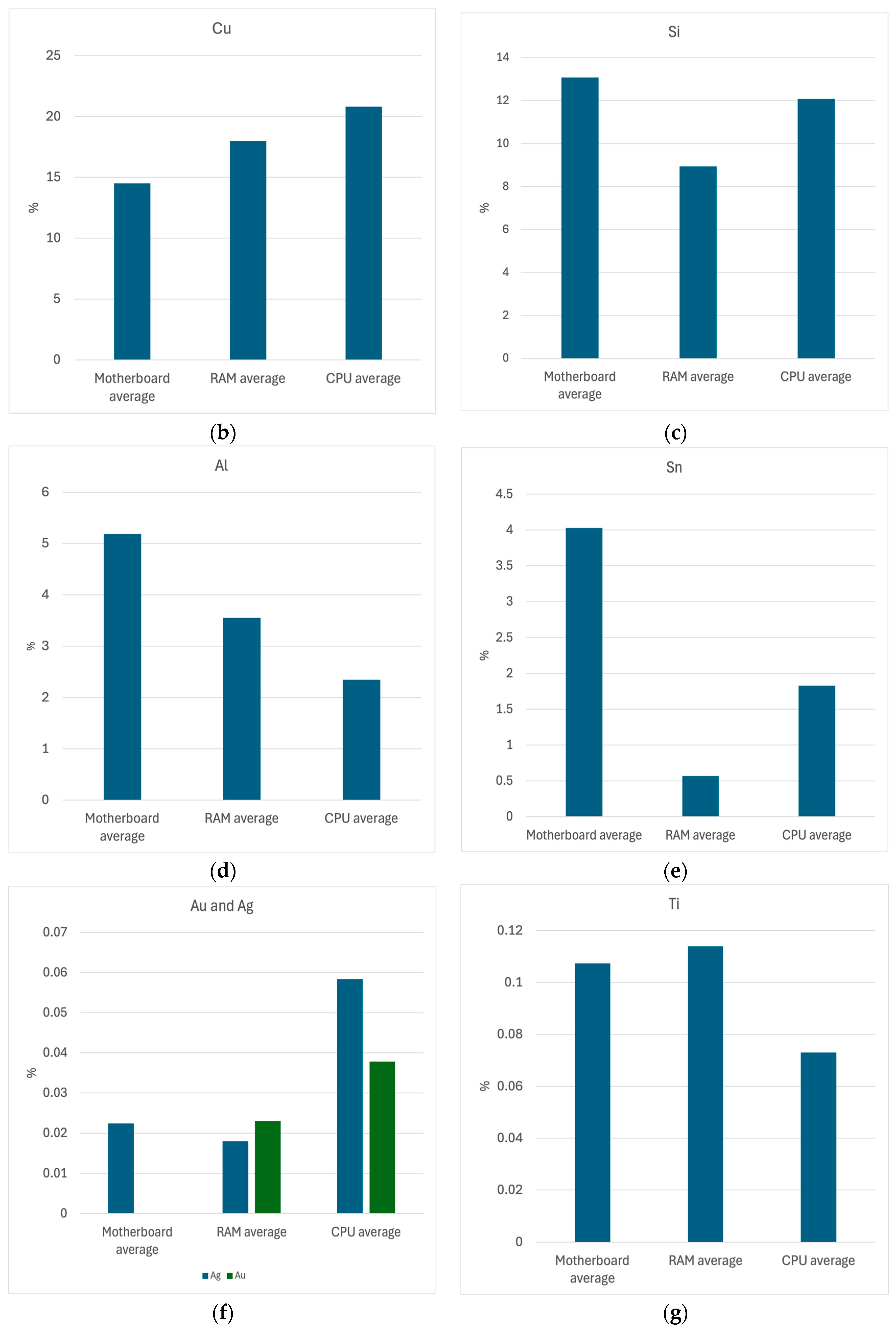
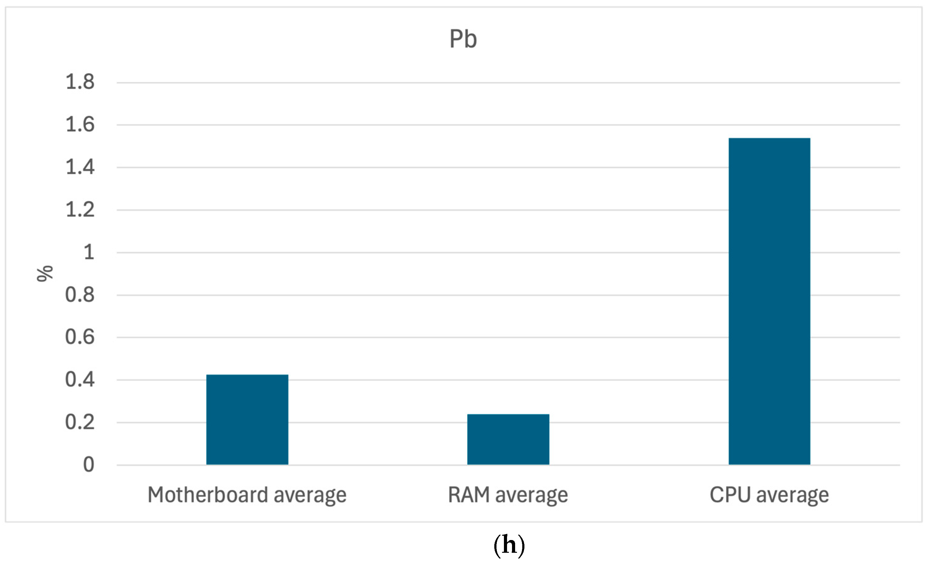
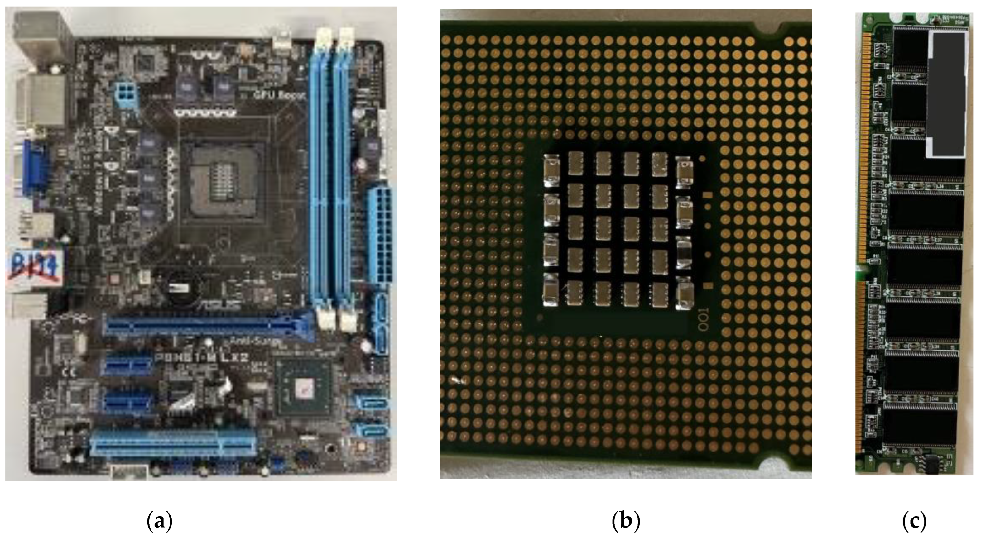
2.1. Characterization of the Various Categories of PCBs

The data obtained from the investigation of the three different types of PCBs bridge the gap in our knowledge about the differences in the composition between the various types of PCBs. To ensure the data is valuable, it is essential to compare the average content of materials that are economically important or present in large quantities. The average material composition of the three PCB types, based on the XRF analysis data, shows that all three types primarily contain the same materials: copper, silicon, tin, calcium, and aluminum, as shown in Figure 1a.
For these dominant materials, ANOVA tests were carried out. The tests reveal that both copper and silicon are statistically representative and that there is no difference among the three PCB categories, i.e., F < Fcritical. As for tin, aluminum, and calcium, the ANOVA tests have opposite results, meaning that they are not statistically representative, with F > Fcritical. This is especially interesting since the pretreatment and leaching section of this study is focused on copper, thus confirming the representativeness of the results obtained hereafter.
Regarding the presence of copper, which is the most prevalent material in all three analyzed types, CPUs and chipsets are the richest in copper with an average percentage of 20.8%, followed by RAMs at 17.8%, with motherboards showing the lowest amount at only 14.5%, as shown in Figure 1b.
Silicon is most abundant in motherboards, accounting for 13%, although it is present in similar quantities in both RAMs and CPUs, as shown in Figure 1c. In contrast, motherboards are a significant source of aluminum and tin. As shown in Figure 1d, the average aluminum content in motherboards is nearly double that of CPUs and 1.5 times greater than in RAMs. For tin, as depicted in Figure 1e, motherboards are particularly rich, followed by CPUs, which contain approximately half the tin content of motherboards, and RAM, which has a relatively low tin content.
A detailed analysis of the average individual material compositions reveals that CPUs and chipsets are particularly enriched in copper, gold, and silver, while also exhibiting elevated levels of lead. As shown in Figure 1f, the gold content in CPUs and chipsets is approximately twice the average amount found in RAMs, and the silver content is nearly three times higher than that in motherboards, with an even greater disparity when compared to RAMs. The presence of titanium in RAMs and motherboards is worth noting given the importance of titanium as a critical raw material within the EU, as shown in Figure 1g, especially in the case of motherboards, which although contain less than that of the RAMs in terms of quantity, are actually higher since motherboards are usually heavier in weight than RAMs.
Finally, the average lead content in CPUs and chipsets is eightfold that in RAMs and sixfold the average found in motherboards, as shown in Figure 1h. This underlines the importance of correctly treating CPUs and chipsets and employing extra protective procedures to safeguard both the workers and the environment, especially since such elevated levels also surpass those allowed by European regulations. A detailed analysis of each category of the PCBs studied is provided in the supplementary material [43,44].

2.2. Effect of Solvent Pretreatment of Waste PCBs Using DMSO

Waste PCBS were first analyzed to determine their material composition and allow for a better understanding of the effect of the subsequent pretreatment and leaching process. The composition of the waste motherboard PCB mixture goes hand in hand with the discussed results in the previous section. The detailed characterization is shown in Table 2.

2.2.1. Effect of Pretreatment on the Organic Element

The inspection of the pretreated motherboard PCBs using DMSO showed that the organic part, made of resin and glass fibers, is separated from the metals. This swelling effect is seen in both Group 1 with particle sizes between 8 mm and 5.6 mm and Group 2 with particle sizes between 5.6 mm and 2 mm. However, for Group 3 with particle sizes of less than 400 μm, the swelling effect is not visually detectable by eye inspection. Images of the pretreated samples from Group 2 before and after are shown in Figure 2a and b, respectively, and those of Group 3 before and after are shown in Figure 2c and d, respectively.
Further analysis of the treated sample groups was carried out to assess the effect of DMSO on the organic. The calcination process is performed under the conditions mentioned in Section 3.3 as part of the sample preparation process for the chemical analysis.
The analysis of all three category groups showed limited to no change in the organic content loss before and after the solvent treatment, as expected from the solvent pretreatment phase using DMSO. For instance, Group 1 had a weight loss percentage representing the organic content equal to 26.7% and 28% before and after treatment, respectively. Similar behavior was exhibited by both Groups 2 and 3, where Group 2 had an organic content of 26.8% and 27% before and after solvent treatment, respectively, while Group 3 had an organic content of 21.8%, which remained constant during the solvent treatment process. This confirmed the results seen visually in Figure 2, which shows that the resin is swollen, liberating the metal particles; however, the resin is not removed. The swelling of the material during the solvent pretreatment phase, along with the release of metal particles, improves the leaching efficiency, as discussed in the following section.
Similarly, the analysis of the inorganic components in the samples, before and after solvent pretreatment, exhibits negligible changes. This stability can be attributed to the heterogeneous nature of the samples.

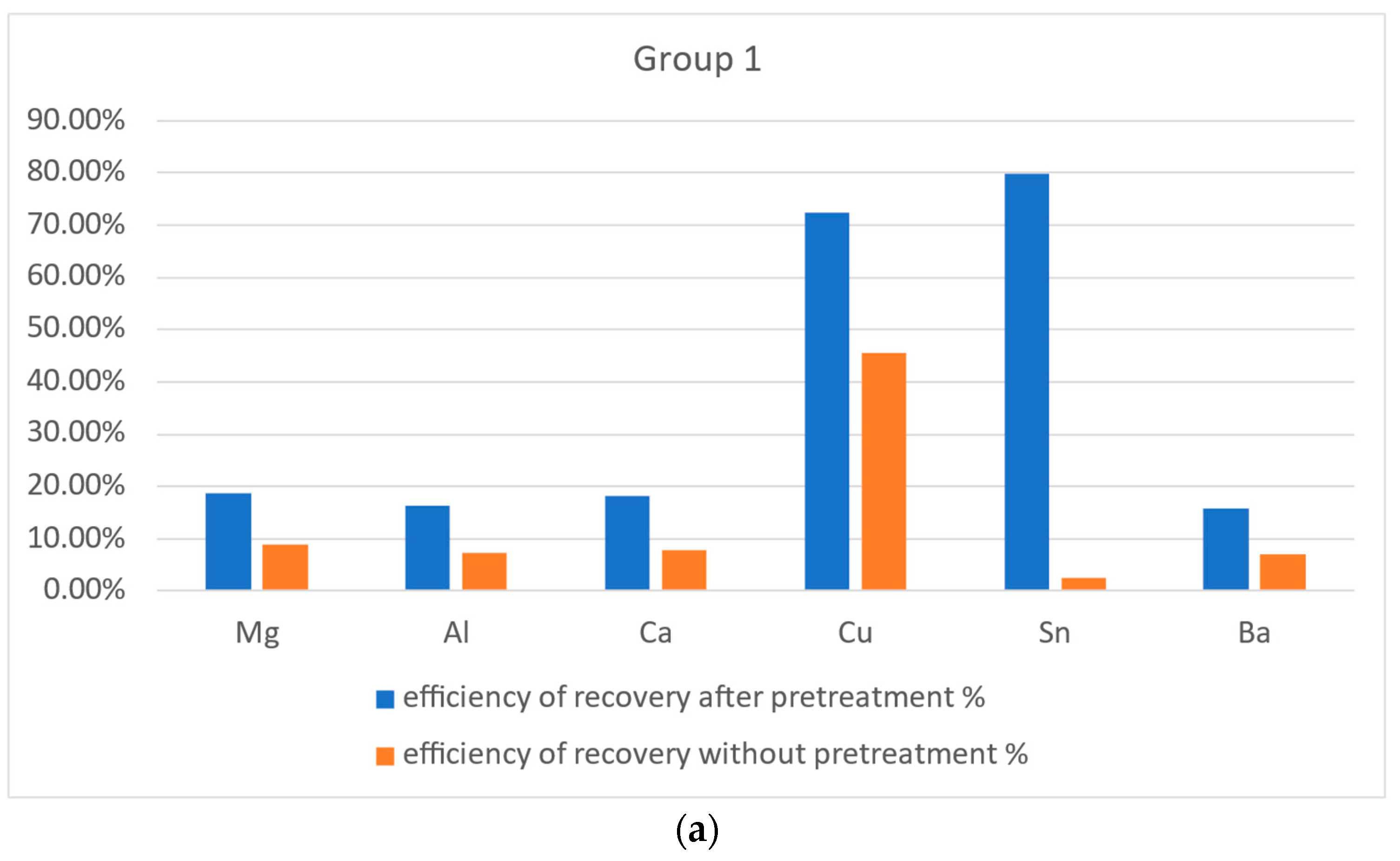
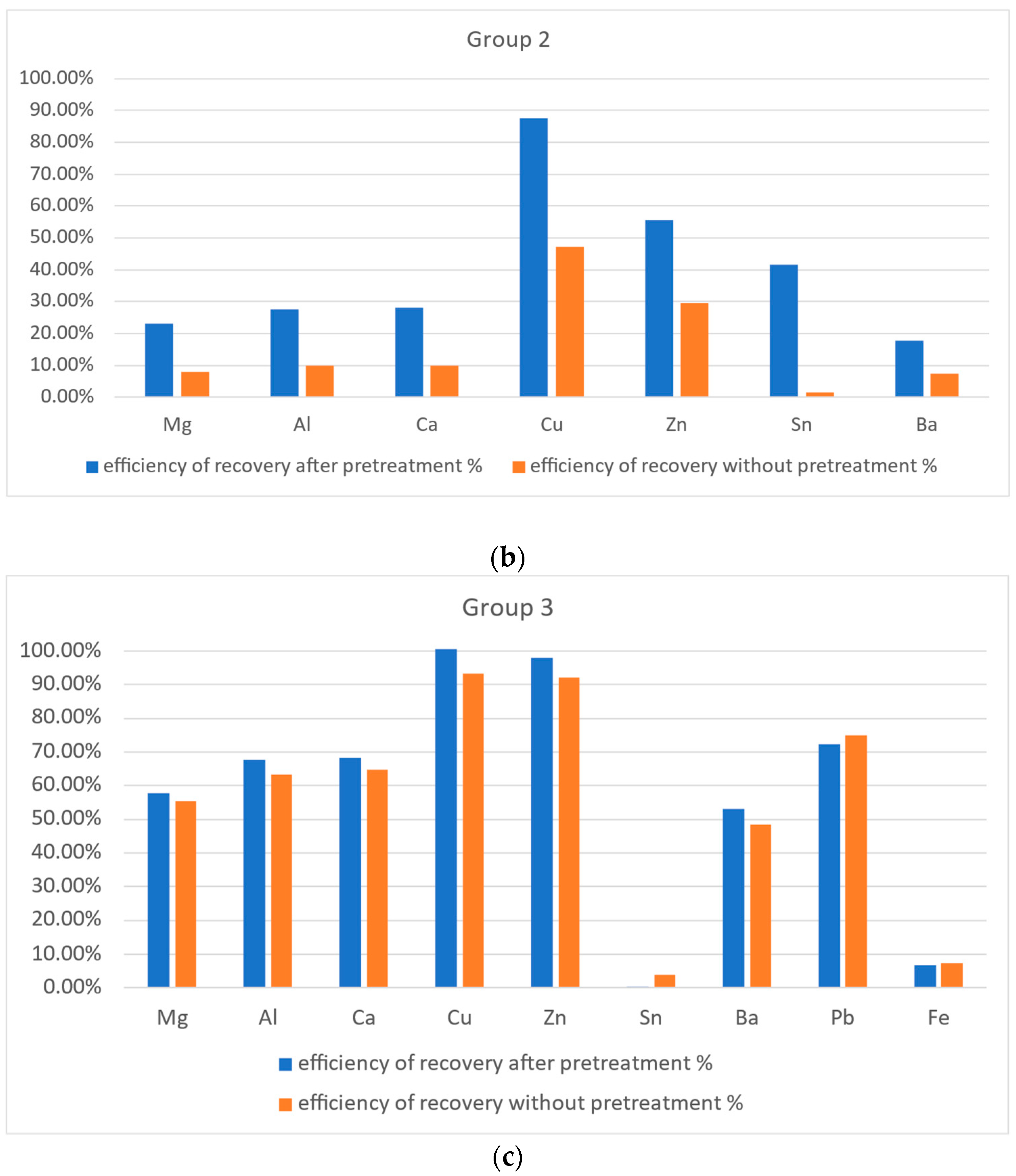
2.2.2. Effect of Pretreatment on Copper Extraction Efficiency During Leaching

During the preparation of the experiment, different agitation speeds were tested. Agitation between 400 and 510 rpm was empirically found to be best and was subsequently used to carry out leaching experiments. This optimized agitation speed was based on the speed that allowed constant and smooth spinning of the magnetic stirring anchor without any disturbances to the flow. Regarding the copper recovery efficiency for the three sample groups, a significant improvement was noted in the case of solvent-treated samples. For instance, in the case of Group 1, the extraction efficiency rises from 45.5% without solvent treatment to 72.4% after being subjected to solvent treatment. In the case of Group 2, the copper recovery efficiency improved from 47.3% to 87.65% after the sample was treated with DMSO before the leaching process. Finally, for Group 3, the improvement in copper recovery efficiency during the leaching process is less staggering, yet it rises from 93.24% to a 100% copper recovery.
The results obtained go hand in hand with the literature regarding the hypothesis that pretreatment using DMSO as a solvent improves the copper recovery efficiency during leaching. Moreover, they provide a deeper understanding of the relationship between particle size and solvent treatment. In that case, the effect of solvent treatment is more visible on larger particle sizes than on fine grains, which can be seen from the almost 30% increase in efficiency in the case of larger particles (Group 1 and Group 2) compared to the 7% increase in case of fine grains (Group 3), in which case the additional use of resources might not be fully justifiable.
The ICP analysis also showed an increase in the efficiency of recovery of other metals present during the leaching process using nitric acid. The increase also followed the same trend as copper, where the effect of solvent treatment was more evident in larger-sized particles (Group 1 and Group 2) than in finer-sized particles (Group 3). The results are shown in Figure 3. In Figure 3a, the recovery efficiency is almost doubled in the case of magnesium, aluminum, calcium, and barium. For tin, the efficiency increases 40-fold. For Group 2, the efficiency doubles for zinc and triples for magnesium, aluminum, calcium, and barium, with tin experiencing a dramatic 40-fold increase, as shown in Figure 3b. Finally, for Group 3, with its finer particle size, as shown in Figure 3c, the trend is less drastic, with efficiencies improving slightly, showing the limited impact of solvent treatment on the leaching process.

3. Materials and Methods

3.1. Materials Collection and Preparation

Waste PCBs were obtained from personal computers used at the Politecnico di Torino, Italy. The retrieved PCBs were 9 motherboards, 10 Random Access Memories (RAMs), and 11 Central Processing Units (CPUs) and chipsets. The PCBs were mostly produced between 2001 and 2011.
The electronic components mounted on the PCBs were desoldered and removed manually via the indirect heating of the PCBs to fuse the soldering and ease the dismounting of the components, leaving the stripped PCB base, which is a substrate sandwich of glass fibers, metals, and resin. The CPU and RAM were cut manually into 1 cm wide strips and then reduced in size using a universal mill in preparation for their analysis. As for the motherboards, a counter-rotating blade mill was first used to reduce the size of the particles to 5.6 mm. Then, further pulverization of the motherboard PCBs was carried out following the same procedure for the CPU and RAM. At each stage, the particle size was checked using sieves to ensure a homogeneous particle size among the samples. The sieves used were 8 mm, 5.6 mm, and 2 mm. In Figure 4, the samples of the different analyzed PCBs are shown. Each sampled PCB was categorized into one of three categories in the scope of this study. Then, the weight of the stripped PCB was measured and the year of production was researched in the cases where it could be identified. To evaluate the effect of pretreatment on copper leaching, the sourced motherboards were all mixed during the shredding process to guarantee a good blend together and were then used for pretreatment and leaching. The material composition was characterized both before and after the treatment processes, identifying the materials contained in each sample and at each change, which allowed us to compare the effect of the pretreatment on leaching.

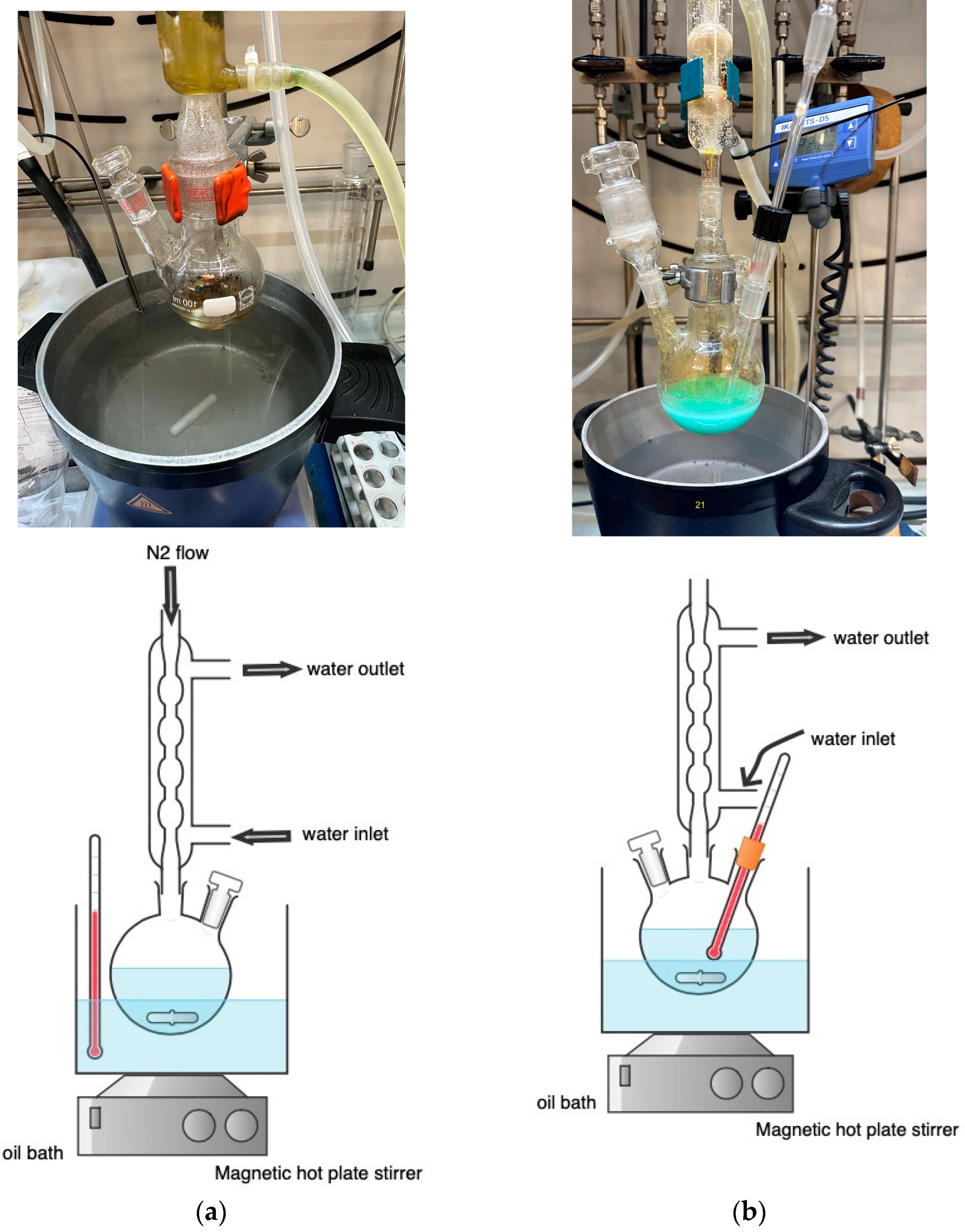
3.2. Pre-Treatment and Leaching Method

The pretreatment phase was applied with the aim of swelling the resin and liberating the metals for the subsequent leaching phase. The optimized pretreatment conditions were those reported by [25] for a particle size of 1–1.5 cm2, which uses DMSO, 1:2 (w/v) at 90 °C for 60 min under constant N2 flow. Those conditions were chosen as they do not require a long heating time at elevated temperatures. The agitation for the process was established at 400–460 rpm using a heating magnetic stirrer. After the pretreatment, the sample was left to dry overnight in a vacuum furnace at 35 °C. Then, part of the sample was taken for analysis following the previously elaborated process for the ICP and XRF and the rest of the sample was used for leaching.
The leaching process, as established by [36], uses nitric acid (HNO3) with a concentration of 3 M and 75 g/L pulp density at 75 °C for 120 min. The chemicals used for the solvent pretreatment and the leaching process were all of lab grade.
The experimental setup for both the solvent pretreatment and the leaching process can be seen in Figure 5a, and Figure 5b, respectively. For the solvent pretreatment process, a double-necked round bottom flask was connected to the top of the cooling system using running water and the N2 flow in an open system setup. The flask was immersed in a hot oil bath with temperature control. Regarding the leaching process, a triple-necked round bottom flask of 250 mL was connected to the top of the cooling system using running water in an open system setup. One of the side openings was fitted with a thermometer for temperature control and the other was used to add the sample. The flask was also immersed in a hot oil bath, like the setup of the solvent pretreatment.
The investigation of the effect of solvent pretreatment on the efficiency of leaching was carried out on 3 different particle size ranges; the first group (hereafter referred to as Group 1) had a particle size between 8 mm and 5.6 mm, the second group (hereafter referred to as Group 2) had a particle size between 5.6 mm and 2 mm, and the final group (hereafter referred to as Group 3) contained fine particles with sizes of less than 400 μm. These size groups were chosen based on the gap identified in the literature where the finest particle size of PCBs to be studied for pretreatment was 6 mm [22]. Thus, the first group was large and covered what has been performed in the literature. Group 2 was chosen as it is an intermediate between the fine particle size and the large size reported in the literature. Group 3 was chosen to compare the difference between a powder state and a coarser particle size, which does not suffer from the hazards of handling fine powders. For each group, a sample was prepared and then a part was analyzed to obtain the material content of the untreated sample. Next, the part was pretreated with a subsequent analysis of part of the sample to study the effect of solvent pretreatment. Finally, the pretreated sample underwent leaching and was then analyzed. To study the effect of solvent pretreatment, a part of the originally prepared untreated sample for each group was taken and directly treated by the established leaching process, allowing a comparison of the results with those that underwent pretreatment. A visual representation of the experiments can be seen in Figure 6.

3.3. Analytical Methods

The sampled PCBs were analyzed using Inductively Coupled Plasma Optical Emission Spectrometry (ICP-OES), Inductively Coupled Plasma Mass Spectrometry (ICP-MS), and X-ray fluorescence spectroscopy (XRF- Axion, Panalytical). For the analysis, the samples were prepared using the previously mentioned process until a fine powder was obtained.
In addition, statistical analysis of the different PCB categories was carried out using the data analysis extension of Excel V.16.89.1, and ANOVA (Analysis-Of-Variance) tests were performed to evaluate the linear correlations among the materials found in the different categories of PCBs, considering only the ones with values F greater than Fcritical as significant.

4. Conclusions

The objectives established for this study were to investigate the effect of solvent pretreatment on the efficiency of the subsequent leaching process, optimizing the process conditions. This study offers a better understanding of the role that particle size plays in the efficiency of material recovery using DMSO as a solvent pretreatment, bridging the gap in the literature. Although fine particle sizes such as in Group 3 have higher copper recovery efficiency even without the pretreatment step, this method continues to demonstrate favorable results, especially with larger particle sizes, which may help eliminate the need for pulverization and lower the amount of material lost during the pulverizing and transportation process. However, there remains a set of challenges that require further improvements, such as solvent recovery and reuse and the scaling of the current solvent treatment method from the lab scale to an industrial scale. Finally, although DMSO is considered a green solvent, it is not completely eco-friendly. Ongoing research is investigating the use of other green solvents, such as ionic liquids, as alternatives.
This study also investigates the different categories of PCBs and the extent of variation in the material composition among the different categories and models, which helps to better target the extraction of those materials and improve the material recovery rates. The results obtained also show through the ANOVA tests carried out that the different categories are statistically representative when it comes to copper and silicon; however, this is not valid for aluminum, tin, and calcium. The study is in line with the goals of a green circular economy, encouraging urban mining and supporting the recent EU Critical Raw Materials act. The results show that silicon, copper, calcium, and aluminum have an overall dominance in the composition of the different categories and models, despite being present in various percentages.
For future work, we aim to deepen the understanding of the changes undergone by raw materials during the pretreatment and leaching phases by studying the microstructure of the PCBs at each phase. Further scaling up of the study from the lab scale to bench and pilot scales is also planned so as to continue assessing the feasibility of this method on an industrial scale.

Supplementary Materials

The following supporting information can be downloaded at: https://www.mdpi.com/article/10.3390/recycling10030080/s1, Figure S1. The relation between the motherboard weight in grams and the present unit market price in Euros of the motherboards was analyzed. The code of each PCB includes its year of production; Figure S2. The relation between copper content in % and the present unit market price in Euros of the motherboards was analyzed. The code of each PCB includes its year of production; Figure S3. The relation between silver content in % and the unit price of the motherboards in Euros; Figure S4. The material composition of the 9 analyzed motherboard PCBs. The production years of motherboards are indicated between brackets and the thickness of size of the bars represent the amount of material percentage in the sample; Figure S5. Material composition of the 10 analyzed RAM and the average material content. The year of production of each analyzed RAM is shown between parenthesis and the size of the bar represents the material presence within the sample; Figure S6. Visualization of the impact of gold and silver content on the current unit price of the RAM in Euros; Figure S7. Visualization of the relation between the tin content in the analyzed RAMs and their current unit price in Euros; Figure S8. Visualization of the trends in material content of the analyzed RAM showing the fluctuations and unsteady trends. In figure (a) the material content is shown on a log scale while in (b) the graph represents the content percentage of each material; Figure S9. Graphical representation of the material content of the four most present materials in the analyzed RAM samples. The graph is shown in log scale of the content percentage of each material; Figure S10. The material composition of the 11 analyzed CPUs and chipsets; Figure S11. Graphical representation of the gold and silver content in the different analyzed CPUs and chipsets; Table S1. The material composition of the 9 analyzed motherboard PCBs using XRF; Table S2. Material composition of the 10 analyzed RAM PCBs using XRF; Table S3. The material composition of the 11 analyzed CPUs and chipsets using XRF.

Author Contributions

Conceptualization, A.T.I.M., G.S. and F.R.; methodology, A.T.I.M., G.S. and F.R.; software, A.T.I.M.; validation, A.T.I.M., G.S. and F.R.; formal analysis, A.T.I.M., G.S. and F.D.; investigation, S.P. and G.C.; resources, A.T.I.M., G.S., S.P. and G.C.; data curation, A.T.I.M., S.P. and G.C.; writing—original draft preparation, A.T.I.M. and F.D.; writing—review and editing, F.D. and F.L.; visualization, A.T.I.M. and F.D.; supervision, F.L., D.F. and F.R.; project administration, F.L., D.F. and F.R.; funding acquisition, F.L. All authors have read and agreed to the published version of the manuscript.

Funding

This research was funded by Eni S.p.A. and the NODES project, which received funding from the MUR–M4C2 1.5 of PNRR funded by the European Union—Next Generation EU (grant agreement no. ECS00000036).

Data Availability Statement

The original contributions presented in this study are included in the article/supplementary material. Further inquiries can be directed to the corresponding author.

Acknowledgments

A.T.I.M. and F.L. acknowledge financial support by Eni S.p.A.

Conflicts of Interest

Author Giuliana Schimperna, Gianluca Cantoni, Sara Perucchini and Francesca Rubertelli were employed by the company Eni SpA. The remaining authors declare that the research was conducted in the absence of any commercial or financial relationships that could be construed as a potential conflict of interest.

Abbreviations

CPUCentral Processing Unit
DMA Dimethylacetamide
DMF Dimethylformamide
DMSO Dimethyl sulfoxide
ICP-MSInductively Coupled Plasma Mass Spectrometry
ICP-OESInductively Coupled Plasma Optical Emission Spectrometry
NMP N-methyl-2-pyrrolidone
PBDE Polybromodiphenylethers
PC Personal computer
PCBPrinted circuit Boards
RAMRandom Access Memory
REMRare-earth metals
TBBPA Tetrabromobisphenol A
WEEE Waste Electrical and Electronic Equipment
XRFX-ray fluorescence spectroscopy

References

  1. Kumar, A.; Holuszko, M.; Crocce, D.; Espinosa, R. E-waste: An overview on generation, collection, legislation and recycling practices. Resour. Conserv. Recycl. 2017, 122, 32–42. [Google Scholar] [CrossRef]
  2. Cui, J.; Zhang, L. Metallurgical recovery of metals from electronic waste: A review. J. Hazard. Mater. 2008, 158, 228–256. [Google Scholar] [CrossRef] [PubMed]
  3. Hall, W.J.; Williams, P.T. Separation and recovery of materials from scrap printed circuit boards. Resour. Conserv. Recycl. 2007, 51, 691–709. [Google Scholar] [CrossRef]
  4. European Commission. A New Circular Economy Action Plan for a Cleaner and More Competitive Europe; European Commission: Brussels, Belgium, 2020. Available online: https://eur-lex.europa.eu/legal-content/EN/TXT/?uri=CELEX:52020DC0098 (accessed on 5 November 2024).
  5. European Commission. Critical Raw Materials. Available online: https://single-market-economy.ec.europa.eu/sectors/raw-materials/areas-specific-interest/critical-raw-materials_en (accessed on 29 October 2024).
  6. European Parliament. Directive 2012/19/EU on Waste Electrical and Electronic Equipment (WEEE); European Parliament: Brussels, Belgium, 2012; pp. 38–71. Available online: https://eur-lex.europa.eu/legal-content/EN/TXT/?uri=CELEX:32012L0019 (accessed on 2 July 2024).
  7. Priya, A. Management of Electronic Waste: Resource Recovery, Technology and Regulation; Wiley: Hoboken, NJ, USA, 2023; Available online: https://www.wiley.com/en-us/Management+of+Electronic+Waste%3A+Resource+Recovery%2C+Technology+and+Regulation-p-9781119894339 (accessed on 16 January 2024).
  8. Oke, E.A.; Potgieter, H. Recent chemical methods for metals recovery from printed circuit boards: A review. J. Mater. Cycles Waste Manag. 2024, 26, 1349–1368. [Google Scholar] [CrossRef]
  9. Trinh, H.B.; Kim, S.; Lee, J. Selective Copper Recovery by Acid Leaching from Printed Circuit Board Waste Sludge. Metals 2020, 10, 293. [Google Scholar] [CrossRef]
  10. Liu, J.C.; Kao, T.-H. Extraction of Cu and Pb from printed circuit board sludge using ammonia solutions. Water Sci. Technol. 2003, 47, 167–172. [Google Scholar] [CrossRef]
  11. Kumar, M.; Lee, J.-C.; Kim, M.-S.; Jeong, J.; Yoo, K. Leaching of metals from waste printed circuit boards (WPCBs) using sulfuric and nitric acids. Environ. Eng. Manag. J. (EEMJ) 2014, 13, 2601–2607. [Google Scholar] [CrossRef]
  12. Ilyas, S.; Anwar, M.A.; Niazi, S.B.; Afzal Ghauri, M. Bioleaching of metals from electronic scrap by moderately thermophilic acidophilic bacteria. Hydrometallurgy 2007, 88, 180–188. [Google Scholar] [CrossRef]
  13. Birloaga, I.; De Michelis, I.; Ferella, F.; Buzatu, M.; Vegliò, F. Study on the influence of various factors in the hydrometallurgical processing of waste printed circuit boards for copper and gold recovery. Waste Manag. 2013, 33, 935–941. [Google Scholar] [CrossRef]
  14. Tuncuk, A.; Stazi, V.; Akcil, A.; Yazici, E.Y.; Deveci, H. Aqueous metal recovery techniques from e-scrap: Hydrometallurgy in recycling. Miner. Eng. 2012, 25, 28–37. [Google Scholar] [CrossRef]
  15. Oke, E.A.; Potgieter, H. Discarded e-waste/printed circuit boards: A review of their recent methods of disassembly, sorting and environmental implications. J. Mater. Cycles Waste Manag. 2024, 26, 1277–1293. [Google Scholar] [CrossRef]
  16. Cui, J.; Forssberg, E. Mechanical recycling of waste electric and electronic equipment: A review. J. Hazard. Mater. 2003, 99, 243–263. [Google Scholar] [CrossRef]
  17. Charitopoulou, M.A.; Papadopoulou, L.; Achilias, D.S. Removal of Bromine from Polymer Blends with a Composition Simulating That Found in Waste Electric and Electronic Equipment through a Facile and Environmentally Friendly Method. Polymers 2023, 15, 709. [Google Scholar] [CrossRef]
  18. Guo, X.; Peng, S.; Jiang, L.; Mo, X.; Zhu, Y.; Liu, Y.; Cai, K.; Song, Q. Removal of polybrominated diphenyl ethers in high impact polystyrene (HIPS) from waste TV sets. Environ. Sci. Pollut. Res. 2022, 29, 59317–59327. [Google Scholar] [CrossRef]
  19. Schlummer, M.; Popp, L.; Trautmann, F.; Zimmermann, D.; Maurer, A. Recovery of bromine and antimony from WEEE plastics. In Proceedings of the 2016 Electronics Goes Green 2016+ (EGG), Berlin, Germany, 6–9 September 2016; IEEE: Piscataway Township, NJ, USA; pp. 1–5. [Google Scholar] [CrossRef]
  20. Zhu, P.; Chen, Y.; Wang, L.Y.; Zhou, M.; Zhou, J. The separation of waste printed circuit board by dissolving bromine epoxy resin using organic solvent. Waste Manag. 2012, 33, 484–488. [Google Scholar] [CrossRef] [PubMed]
  21. Council, B.; Haarman, A.; Fedato, S.; Holt, A. Brominated Flame Retardants and the Circular Economy of WEEE Plastics State of Play. 2023. Available online: https://www.bsef.com/wp-content/uploads/2023/09/Brominated-Flame-Retardants-and-the-Circular-Economy-of-WEEE-Plastics.pdf (accessed on 19 January 2024).
  22. Wath, S.B.; Katariya, M.N.; Singh, S.K.; Kanade, G.S.; Vaidya, A.N. Separation of WPCBs by dissolution of brominated epoxy resins using DMSO and NMP: A comparative study. Chem. Eng. J. 2015, 280, 391–398. [Google Scholar] [CrossRef]
  23. Verma, H.R.; Singh, K.K.; Mankhand, T.R. Dissolution and separation of brominated epoxy resin of waste printed circuit boards by using di-methyl formamide. J. Clean. Prod. 2016, 139, 586–596. [Google Scholar] [CrossRef]
  24. Verma, H.R.; Singh, K.K.; Mankhand, T.R. Delamination mechanism study of large size waste printed circuit boards by using dimethylacetamide. Waste Manag. 2017, 65, 139–146. [Google Scholar] [CrossRef]
  25. Zhu, P.; Chen, Y.; Wang, L.; Qian, G.; Zhang, W.; Zhou, M.; Zhou, J. Dissolution of Brominated Epoxy Resins by Dimethyl Sulfoxide To Separate Waste Printed Circuit Boards. Environ. Sci. Technol. 2013, 47, 2654–2660. [Google Scholar] [CrossRef]
  26. Zhu, P.; Chen, Y.; Wang, L.Y.; Qian, G.R.; Zhou, M.; Zhou, J. A novel approach to separation of waste printed circuit boards using dimethyl sulfoxide. Int. J. Environ. Sci. Technol. 2013, 10, 175–180. [Google Scholar] [CrossRef]
  27. Kang, K.D.; Ilankoon, I.; Chong, M.N.; Wu, T.Y. Exfoliation of coarse printed circuit boards using dimethylacetamide: Production of copper concentrates. Miner. Eng. 2023, 191, 107963. [Google Scholar] [CrossRef]
  28. Preetam, A.; Modak, A.; Jadhao, R.; Naik, S.N.; Pant, K.K.; Kumar, V. A comprehensive study on the extraction of transition metals from waste random access memory using acetic acid as a chelating solvent. J. Environ. Chem. Eng. 2022, 10, 2213–3437. [Google Scholar] [CrossRef]
  29. Calgaro, C.O.; Schlemmer, D.F.; Bassaco, M.M.; Dotto, G.L.; Tanabe, E.H.; Bertuol, D.A. Supercritical extraction of polymers from printed circuit boards using CO2 and ethanol. J. CO2 Util. 2017, 22, 307–316. [Google Scholar] [CrossRef]
  30. Sanyal, S.; Ke, Q.; Zhang, Y.; Ngo, T.; Carrell, J.; Zhang, H.; Dai, L.L. Understanding and optimizing delamination/recycling of printed circuit boards using a supercritical carbon dioxide process. J. Clean. Prod. 2013, 41, 174–178. [Google Scholar] [CrossRef]
  31. de Souza, G.B.M.; Pereira, M.B.; dos Santos, L.F.; Alonso, C.G.; Jegatheesan, V.; Cardozo-Filho, L. Management of waste printed circuit boards via supercritical water technology. J. Clean. Prod. 2022, 368, 133198. [Google Scholar] [CrossRef]
  32. Suslavich, B.T.; Das, A.; Young, C.A. Chemical Liberation of Waste Printed Circuit Boards. WO2022178235A1, 25 August 2022. Available online: https://patents.google.com/patent/WO2022178235A1/en (accessed on 23 September 2024).
  33. Kaifua, su. Method for Non-Incineration and Non-Cyanation Treatment of Waste Printed Circuit Boards. JP5766305B2, 19 August 2015. Available online: https://patents.google.com/patent/JP5766305B2/en (accessed on 23 September 2024).
  34. Torres Marques, A.; Da Silva Monteiro Bastos, M.M.; Marques Martelo, L.; Soares De Sousa, P.M.; Relvas Vieira Dias, A.C.; Guerreiro Alves Arroja, L.M. Eco-Friendly Method for Recycling Electronic Waste. WO2022123438A1, 16 June 2022. Available online: https://patents.google.com/patent/WO2022123438A1/en (accessed on 23 September 2024).
  35. Ma, L.; Shi, Y.; Wang, Q.; Liang, X.; Li, Z.; Liu, L. Method for Harmless Treatment and Resource Comprehensive Recovery of Circuit Board. CN103084369A, 8 May 2013. Available online: https://patents.google.com/patent/CN103084369A/en (accessed on 23 September 2024).
  36. Dutta, D.; Panda, R.; Kumari, A.; Goel, S.; Jha, M.K. Sustainable recycling process for metals recovery from used printed circuit boards (PCBs). Sustain. Mater. Technol. 2018, 17, e00066. [Google Scholar] [CrossRef]
  37. Vijayaram, R.; Nesakumar, D.; Chandramohan, K. Copper Extraction from the Discarded Printed Circuit Board by Leaching. Res. J. Eng. Sci. 2013, 2, 11–14. Available online: https://www.isca.in (accessed on 29 November 2023).
  38. Sethurajan, M.; van Hullebusch, E.D. Leaching and Selective Recovery of Cu from Printed Circuit Boards. Metals 2019, 9, 1034. [Google Scholar] [CrossRef]
  39. Silvas, F.P.C.; Jiménez Correa, M.M.; Caldas, M.P.K.; de Moraes, V.T.; Espinosa, D.C.R.; Tenório, J.A.S. Printed circuit board recycling: Physical processing and copper extraction by selective leaching. Waste Manag. 2015, 46, 503–510. [Google Scholar] [CrossRef]
  40. Kang, K.D.; Ilankoon, I.M.S.K.; Dushyantha, N.; Chong, M.N. Assessment of Pre-Treatment Techniques for Coarse Printed Circuit Boards (PCBs) Recycling. Minerals 2021, 11, 1134. [Google Scholar] [CrossRef]
  41. Priya, A.; Hait, S. Characterization of particle size-based deportment of metals in various waste printed circuit boards towards metal recovery. Clean. Mater. 2021, 1, 100013. [Google Scholar] [CrossRef]
  42. Priya, A.; Hait, S. Qualitative and quantitative metals liberation assessment for characterization of various waste printed circuit boards for recycling. Environ. Sci. Pollut. Res. 2017, 24, 27445–27456. [Google Scholar] [CrossRef] [PubMed]
  43. Baldé, C.P.; Kuehr, R.; Yamamoto, T.; McDonald, R.; D’Angelo, E.; Althaf, S.; Bel, G.; Deubzer, O.; Fernandez-Cubillo, E.; Forti, V.; et al. “The Global E-waste Monitor 2024”, Geneva/Bonn. 2024. Available online: https://www.itu.int/itu-d/sites/environment (accessed on 16 October 2024).
  44. The European Parliament, Directive 2011/65/EU of the European Parliament and of the Council of 8 June 2011 on the Restriction of the Use of Certain Hazardous Substances in Electrical and Electronic Equipment Text with EEA Relevance. 2011. Available online: https://eur-lex.europa.eu/legal-content/EN/TXT/?uri=CELEX:32011L0065 (accessed on 8 September 2018).
Figure 1. Comparison of the average content of some of the principal materials in different PCB types (Motherboards, CPUs, and RAMs): (a) the overall average composition of three types of PCBs; (b) the average content of copper in different PCB types; (c) the average content of silicon in different PCB types; (d) the average content of aluminum in different PCB types; (e) the average content of tin in different PCB types; (f) the average content of silver and gold in different PCB types; (g) the average content of titanium in different PCB types; and (h) the average content of lead in different PCB types.
Recycling 10 00080 g001aRecycling 10 00080 g001bRecycling 10 00080 g001c
Figure 2. Images of the solvent-pretreated PCB samples: (a) Group 2 with particle size between 5.6 mm and 2 mm before solvent pretreatment; (b) Group 2 with particle size between 5.6 mm and 2 mm after solvent pretreatment; (c) Group 3 with particle size less than 400 μm before solvent pretreatment; and (d) Group 3 with particle size less than 400 μm after solvent pretreatment.
Recycling 10 00080 g002
Figure 3. The effect of solvent treatment on the metal recovery efficiency for different particle sizes: (a) Group 1 with particle size between 8 mm and 5.6 mm; (b) Group 2 with particle size between 5.6 mm and 2 mm; and (c) Group 3 with particle size less than 400 μm.
Recycling 10 00080 g003aRecycling 10 00080 g003b
Figure 4. Samples of the different types of PCBs analyzed: (a) Motherboard PCB; (b) CPU; (c) RAM.
Recycling 10 00080 g004
Figure 5. Experimental setups for the (a) solvent pretreatment process and (b) leaching process.
Recycling 10 00080 g005
Figure 6. A diagram of the experiments carried out to assess the impact of the solvent pretreatment process.
Recycling 10 00080 g006
Table 1. Summary of the solvent pretreatment methods for waste PCBs.
Method UsedType of WEEEParticle SizeTemperatureDurationSolid-To-Liquid RatioReference
DMSOPC-Motherboard16 mm2145 °C60 min1:7Zhu et al. [20]
DMSOPC-Motherboard1–1.5 cm290 °C60 min1:2Zhu et al. [25]
DMSOPC-Motherboard1–1.5 cm2135 °C10 min1:2Zhu et al. [25]
DMSOPC-Motherboard2–3 cm290 °C90 min1:2Zhu et al. [25]
DMSOPC-Motherboard2–3 cm2135 °C20 min1:2Zhu et al. [25]
DMSOPC-Motherboard15–20 mm2170 °C30 min1:2Zhu et al. [26]
DMSOPC motherboard6 mm90 °C90 min1:2Wath et al. [22]
DMAPC-Motherboard1 cm2160 °C75 min1:10Dean Kang et al. [27]
DMAPC-Motherboard1 cm2160 °C150 min3:10Verma et al. [24]
DMAPC-Motherboard16 cm2160 °C420 min3:10Verma et al. [24]
DMFMix PCBs1 cm2135 °C240 min300 g/LVerma et al. [23]
NMPPC motherboard8 mm sieve100 °C90 min1:5Wath et al. [22]
Supercritical ethanolRAM PCB10–20 mm300 °C60 min1:20Preetam et al. [28]
Table 2. The detailed material composition of the waste motherboard PCB mixture used for the pretreatment and leaching tests.
MaterialAlBaBrCaCuFeMgNaPbSSiSnSrTiZnZr
Weight %4.60.60.19.512.70.10.20.20.50.213.33.20.10.20.030.01
Disclaimer/Publisher’s Note: The statements, opinions and data contained in all publications are solely those of the individual author(s) and contributor(s) and not of MDPI and/or the editor(s). MDPI and/or the editor(s) disclaim responsibility for any injury to people or property resulting from any ideas, methods, instructions or products referred to in the content.

