Article

Effect of Si-Based Anode Lithiation on Charging Characteristics of All-Solid-State Lithium-Ion Battery

by
Alexander S. Rudy
1,*,
Sergei V. Kurbatov
1,
Alexander A. Mironenko
1,
Victor V. Naumov
1,
Alexander M. Skundin
2 and
Yulia S. Egorova
1
1
Department of Nanotechnology in Electronics, Physical Faculty, P.G. Demidov Yaroslavl State University, Sovetskaya St., 14, 150003 Yaroslavl, Russia
2
Laboratory of Processes in Chemical Current Sources, Frumkin Institute of Physical Chemistry and Electrochemistry, 31, Leninskii prospect, 119071 Moscow, Russia
*
Author to whom correspondence should be addressed.
Batteries 2022, 8(8), 87; https://doi.org/10.3390/batteries8080087
Submission received: 17 June 2022 / Revised: 18 July 2022 / Accepted: 9 August 2022 / Published: 14 August 2022
(This article belongs to the Special Issue Lithium-Ion Battery Energy Storage Technology)

Abstract

:
The description of the design, manufacturing technology, and test results of thin-film solid-state lithium-ion batteries with a nanocomposite negative electrode Si@O@Al is given herein. This electrochemical system features the hike on the charging curve plateau, which is interpreted as the change from I–V of the Ti-Si@O@Al contact. The latter is due to the change in the type of silicon conductivity during lithiation, as a result of which the ohmic metal-semiconductor contact proves to be biased in the reverse direction, and the charging current is maintained by minority charge carriers. It is shown that the current-conducting component Si@O@Al is formed by a solid solution a-Si(Al), which has a p-type conductivity. The change in the type of conductivity occurs as a result of silicon compensation through lithiation. It was found that Si@O@Al is nonlinear conductor, which can be considered as a percolation cluster formed by amorphous silicon nanoparticles and molecular clusters of silicon dioxide. The height of the Schottky barrier of the Ti|a-Si(Al) contact and the electron affinity of the a-Si(Al) solid solution were estimated.

1. Introduction

All-solid-state thin-film lithium-ion batteries (SSLIB) comprise a separate and a very specific class of batteries [1]. Their appearance was prompted by the demand from the booming industry for microminiature devices, including portable electronics (smart cards, miniature smartphones, microelectromechanical systems (MEMS), wrist gadgets, RFID tags, etc.), medical technology (implantable devices, transdermal patches, and micro robots), and the Internet of Things (IoT). In the course of the further miniaturization of various gadgets, it became necessary to develop micro-batteries and embedded power supplies, i.e., micro-batteries located on the same crystal as the microelectronic devices per se. The difference between the latter and bare die batteries (for instance, CBC005 [2]) is that they are manufactured in the same technological process as the main device, for example, a microcircuit or an electromechanical system. Therefore, the manufacturing technology of the micro-battery must be compatible with that of the main device. This requirement imposes certain restrictions on both the manufacturing technology of the micro-battery and the materials used. That is why the technology behind SSLIBs’ manufacturing is completely different from that of conventional batteries and is mainly based on the magnetron deposition of functional layers.
All-solid-state thin-film batteries have appeared at the very end of the last century, and by now one can find several detailed reviews on this topic [3,4,5,6,7,8]. The first SSLIBs used metallic lithium as the negative electrode, which is extremely inconvenient, especially with respect to thin-film batteries. The reason is that lithium cannot be deposited by magnetron sputtering such as the rest of the SSLIB functional layers. To complete this, the thermal evaporation method is required, and accordingly, one more PVD unit. In addition, metallic lithium is extremely difficult to keep within the functional layer, and over time it penetrates into all the others, including the insulating SiO2 layers. A worthy substitute for lithium is silicon, which has the highest theoretical capacity regarding the reversible insertion of lithium. Nevertheless, a simple replacement of lithium with silicon is hardly possible for a number of reasons of a physical nature, which are widely known [1,9,10,11,12,13,14]. First of all, these are mechanical stresses arising from the introduction of lithium into the crystal lattice, which destroy silicon long before the maximal capacity is reached.
A simple way to overcome this obstacle, described in [15,16,17,18], is an artificial limitation of the capacity by the partial oxidation of silicon. This is achieved by the magnetron sputtering of silicon in an oxygen flow, resulting in the formation of the Si@O@Al nanocomposite. However, the electronic conductivity of such a composite is significantly lower than the conductivity of crystalline and even amorphous silicon (a-Si). To improve the conductivity, about 10 at.% aluminum is added to the Si@Al composite; as a result of which, a three-component nanocomposite material Si@O@Al is formed. The practical application of the Si@O@Al electrode in SSLIBs of various electrochemical systems revealed some features in the charging curves of these batteries. The most salient feature of these curves is the voltage hike in the galvanostatic charge mode, which occurs at a certain degree of lithiation of the negative electrode. It was suggested, and later confirmed experimentally, that the voltage hike is due to the compensation of the acceptor impurity Al by the donor impurity Li. Previously, it was believed that aluminum nanoparticles were only bridging amorphous silicon domains. Subsequent experiments revealed that aluminum impurity provides the hole conductivity of silicon, which is a necessary condition for the lithiation of the electrode to full depth. Thus, in the process of lithiation, the hole semiconductor is initially compensated, and then is doped with a donor impurity Li; as a result of which, the Si@O@Al contact with the Ti downconductor transforms from ohmic to rectifying and reverse-biased. The experimental and theoretical substantiation of these statements enables the main content of this work.
The hole conductivity of Si@O@Al is determined not only by the aluminum concentration, but also by the mode of magnetron deposition of the nanocomposite. Since different Si@O@Al deposition technologies have been used previously, the first item of the experimental section describes the latest technologies that have been used to fabricate Si@O@Al electrodes. The second item of the same section is devoted to the design of L i C o O 2 L i P O N S i @ O @ A l and L i x V 2 O 5 L i P O N S i @ O @ A l prototypes and their manufacturing. The third item presents the results of the prototypes’ testing, which reveals the feature of the charge curves in the form of a hike. In the first item of the discussion section, the structure of the Si@O@Al nanocomposite, various modes of Al insertion into the Si lattice, and the Al impurity contribution to the hole conductivity are considered. The second item explains the rise in downconductor-Si@O@Al resistance with Si@O@Al lithiation from the standpoint of the silicon band structure. It is shown that a change in the Si type of conductivity leads to an increase in the contact resistance and the appearance of a hike on the charge curve. The third item describes the experimental results proving the p-type conductivity of Si@O@Al, which confirms all the assumptions made earlier and the proposed mechanism for the hike formation on the charging curve.

2. Experimental

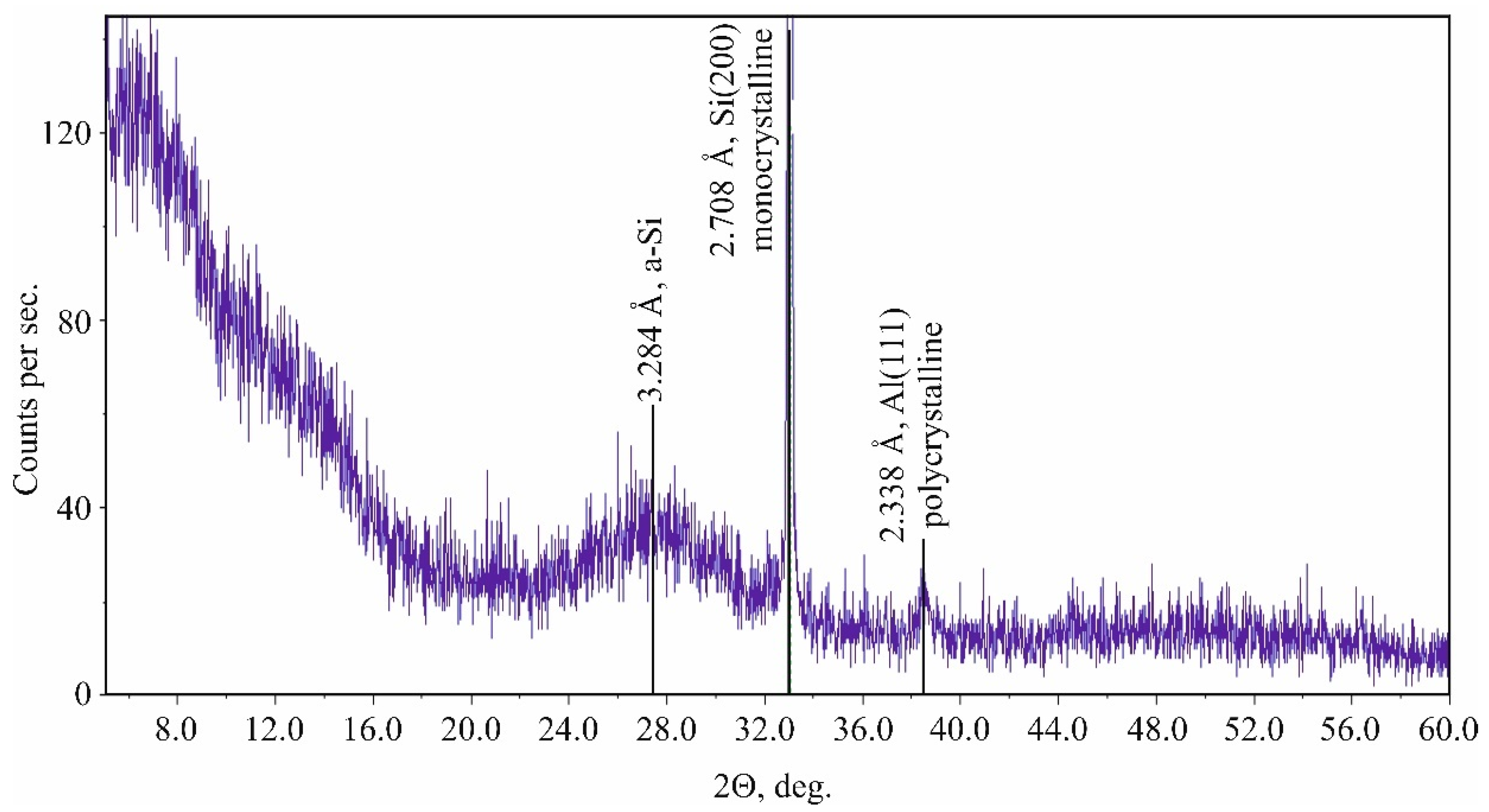
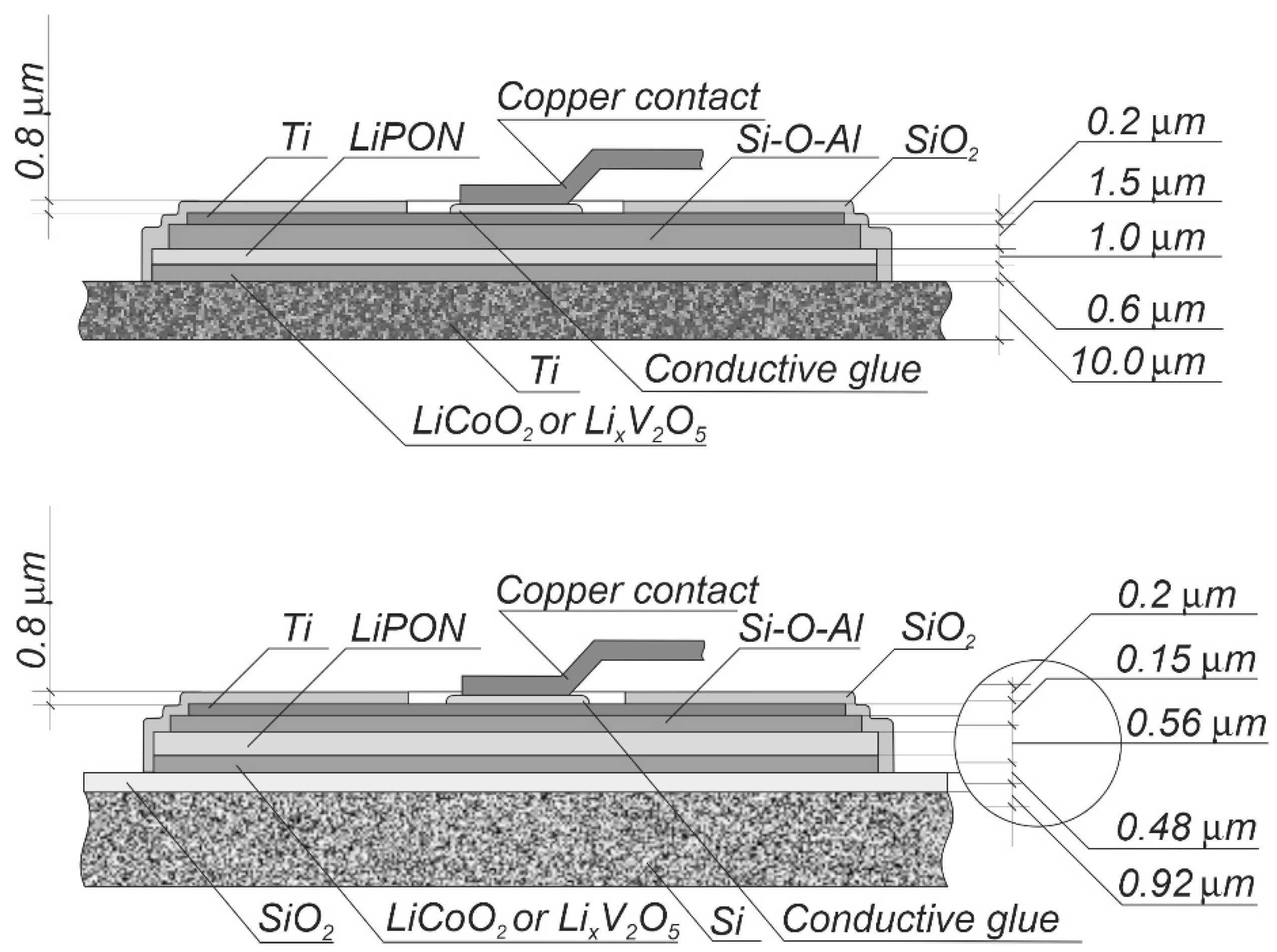
2.1. Si@O@Al Electrode Manufacturing and Characterization

The study of the morphology and of the elemental and phase composition, capacity, and conductivity of negative electrodes was carried out on samples in the form of thin Si@O@Al films deposited on titanium foil and silicon substrates. For Si@O@Al deposition, the following magnetron systems were used:
  • MVU TM Magna 10 (developed by JSC “Research Institute of Precision Machine Manufacturing”, Zelenograd, Russia), equipped with two magnetrons which were used for separate Si and Al depositions;
  • Oratorio 22 system (idem) equipped with four magnetrons connected in pairs.
The choice of the magnetron sputtering method was due to the fact that it provides a high deposition rate and efficient mixing of the sputtered substance at the atomic level. At a high rate of deposition and through good thermal contact with the substrate holder an amorphous silicon (a-Si) is formed, which is less susceptible to destruction under mechanical stress caused by lithium insertion. In the MVU TM Magna 10 system, electrodes were deposited by DC magnetron sputtering. A target made of alloy S i 0.9 A l 0.1 was installed on one magnetron, and a target made of pure aluminum was mounted on the other one. The power of the magnetron on the S i 0.9 A l 0.1 alloy target was constant and amounted to about 600 W, while the power on the aluminum target was switched alternatively from 50 to 200 W in automated regime. By this deposition mode, Si@O@Al films were obtained where layers enriched with aluminum alternated with layers in which the aluminum content was lower. Figure 1 shows the cleavage and surface of a multilayer film. Although Si@O@Al film has a columnar structure, shown in Figure 1, the columns themselves consist of alternating layers, which were well-resolved in Z-contrast regime.
The columnar structure of Si@O@Al promotes lithium diffusion through the entire electrode while layered structure enables a greater number of lithiation-delithiation cycles in liquid electrolytes. Experimental samples of multilayer electrodes demonstrated a capacity of about 2500 mA∙h/g (CLi = 11.3 × 1022 cm−3 or more than 2 Li atoms per Si atom) during 100 cycles [16] and even more. As will be shown below, in SSLIB, the lithium concentration in the electrode is tens of times less than in batteries with liquid electrolyte. Under these conditions, the multilayer electrode can be replaced by a homogeneous one without any loss of stability. Homogeneous electrodes were fabricated on an Oratorio 22 system as test structures for measuring the charge–discharge capacities. Since the manufacturing of homogeneous electrodes is significantly easier than that of multilayered electrodes (Table 1), this technology was adapted for the production of Si@O@Al electrode batches. These electrodes can be stored for years in the atmosphere and are used as blanks for SSLIBs’ manufacture. The technological parameters of Si@O@Al deposition are given in Table 1. In [15,16,17,18], this technology and Si@O@Al’s properties are described in more detail.
The elemental composition of Si@O@Al films was studied by energy dispersive analysis using INCAx-act (Oxford Instruments, Bristol, UK)—a console attachment to a Supra 40 electron microscope—and EDAX (Ametek Inc., Berwyn, Illinois, USA)—an attachment to the Quanta 3D 200i electron microscope with FIB. Table 2 shows the results of the elemental composition analysis for 15 samples of Si@O@Al films. For this analysis only uniform films were used, since the data on multilayer structures, especially at normal incidence of the electron beam, strongly depend on the beam’s penetration depth. To exclude the influence of the silicon substrate in homogenous films, the energy of the electron beam was as low as 5 keV.
The structure and phase composition of Si@O@Al films was studied by X-ray phase analysis on an ARL X’tra X-ray powder diffractometer (Thermo Fisher Scientific, Ecublens, Switzerland). Figure 2 shows the diffraction pattern of a Si@O@Al film on a silicon substrate, on which sharp peaks of a crystalline silicon substrate and a halo from amorphous silicon and nanocrystalline aluminum are clearly visible. Thus, the parameters of magnetron deposition given in Table 1 enable the deposition of Si@O@Al nanocomposite whose powder pattern contains no crystalline diffraction peaks, i.e. look as pattern of amorphous materials. Such materials are referred to as “X-ray amorphous”. The structure of this material and its electrical properties will be discussed below.
The Si@O@Al electrodes’ characterization was carried out in the galvanostatic mode in standard electrochemical test cells with lithium counter and reference electrodes. As the electrolyte, 1 M solution of lithium hexafluorophosphate (LiPF6) in a mixture of ethylene carbonate, diethyl carbonate, and dimethyl carbonate (1:1:1) was used. Figure 3 shows typical charging and discharging curves of a Si@O@Al electrode. As one can see, the composite electrode at relatively low currents can provide a discharge capacity (Cg) of about 2 A·h/g. This corresponds to a surface specific capacity C S = C g ρ h , where ρ 2   g / cm 3 is the film density and h is its thickness. With the usual thicknesses of the negative electrode (1−3 μm), the specific capacity yields CS = 0.4–1.2 mA·h/cm2. It is worth noting that the specific surface capacity Cs is a more important parameter than the gravimetric capacity Cg. An increase in the thickness of silicon-based thin-film electrodes is known to result in a decrease in their gravimetric capacity and in the worsening of their cyclability. Thus, in [19], a gravimetric capacity of 3.5 A·h/g was achieved on silicon films 50 nm thick, and this corresponds to a surface capacity of 0.035 mA·h/cm2. Films 150 nm thick demonstrated a gravimetric capacity of 2200 mA·h/g and a surface capacity of 0.066 mA·h/cm2. In [20], on films 1.5 and 3 µm thick, surface capacities of 0.06 and 0.01 mA·h/cm2 were achieved. The authors of [21] reported on 450 cycles with silicon films with a 340-nm thickness, and only 50 cycles with films of 3.6 µm thickness. Thus, the surface capacitance values obtained in the present work (due to the special structure of thin-film electrodes) are quite impressive.

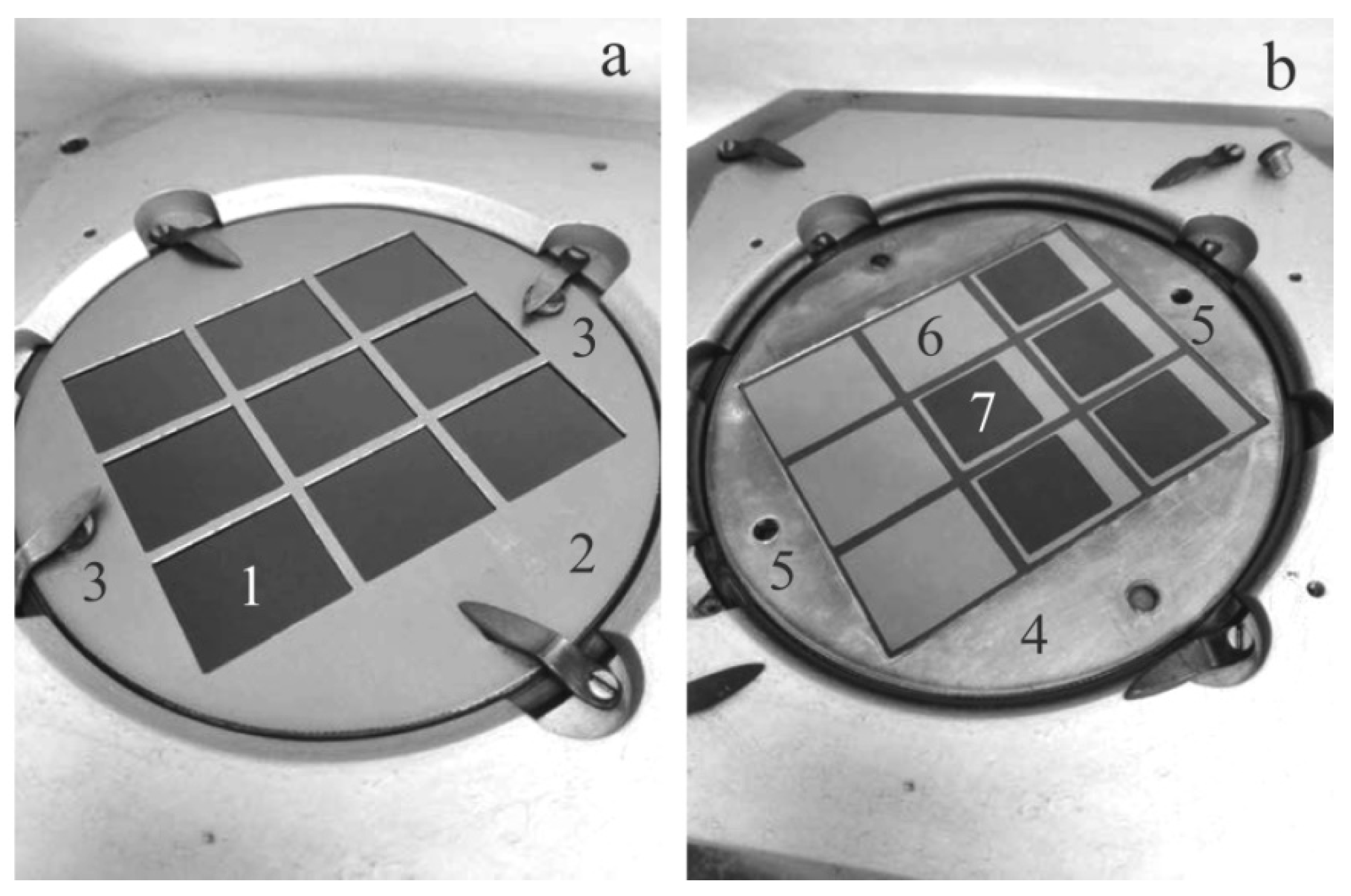
2.2. SSLIB Prototypes Manufacturing

An effect similar to the above described is observed when charging all-solid-state lithium-ion batteries. Unlike a cell with a liquid electrolyte, where the current collector is in contact with the electrolyte and the electrode at the same time, the SSLIB has a clear metal–electrode interface, which greatly facilitates the interpretation of the charging curves. To study the Ti|Si@O@Al contact characteristics, some prototypes of thin-film lithium-ion batteries were made. The electrochemical systems of the batteries L i C o O 2 L i P O N S i @ O @ A l and L i x V 2 O 5 L i P O N S i @ O @ A l differed only by the materials of positive electrode (cathode). Here, LiPON or “Lithium phosphor-oxynitride” is inorganic (ceramic) electrolyte whose composition could be approximately designated as Li3.3PO3.8N0.22. The constructive basis for all prototypes consisted of titanium foil 10 μm thick or a silicon wafer 460 μm thick. The design of titanium and silicon-based SSLIB prototypes is shown in Figure 4. Oтpицaтeльныe элeктpoды cocтaвa Si@O@Al Some functional layers of the SSLIB prototypes were deposited by the SCR-651 “Tetra” magnetron sputtering system. The main reason for the choice of this magnetron system was the possibility of RF sputtering of the cathode materials, which are wide-gap semiconductors and have a very poor conductivity. Sputtering of lithium orthophosphate targets for solid electrolyte deposition also required an RF magnetron. Moreover, this system has 4 magnetrons, which can significantly reduce the interoperative interval during which the lithium-containing functional layers are exposed to atmospheric air. Some of the SSLIBs were manufactured entirely on the SCR-651 “Tetra” system. For example, batteries, in which a lithium-containing electrode was deposited as the first layer, were manufactured only on the SCR-651 “Tetra”, since it was necessary to minimize the time of the lithium-containing electrode’s contact with the atmosphere. On the SCR-651 system, this time was several minutes, which was required to change the mask, while on other systems additional time is necessary to change the target.
To manufacture the SSLIB prototypes, mask technology was used. Rectangular substrates cut from titanium foil or silicon wafer were placed in a mask device, which was attached to a rectangular movable stainless steel substrate holder (Figure 5). The mask device itself consisted of a round mask (2) and a frame (4), which holds the rectangular substrate (1) in a fixed position towards the masks. All elements of the mask device and the copper substrate holder (located under the substrate) had holes (5) for alignment and were fastened to each other using guides (3). The entire structure, through a vacuum lock of the chamber, was placed on a movable substrate holder.
Before deposition, the vacuum chamber was evacuated by a turbomolecular pump to a residual pressure of 5 × 10 7 mbar. Argon (99.9995% purity) was used as a gas for plasma ignition and magnetron sputtering. In the case of L i C o O 2 and Si@O@Al films’ deposition, argon was mixed with oxygen (purity 99.5%). During the LiPON film deposition, the target was sputtered in a nitrogen atmosphere of 99.9999% purity. The substrate was placed above the target face down, and a movable shutter was placed between the target and the substrate. An RF voltage (13.56 MHz) of the required power was applied to the target. At the beginning of each layer’s deposition, the corresponding target was cleaned by sputtering onto the closed shutter, and a few seconds before its opening, an RF bias with a small constant component was applied to the substrate to activate its surface by weak ion bombardment. Immediately before opening the shutter, the bias was turned off. After depositing a film of the required thickness, the shutter was closed. The material deposition rate was calibrated by measuring the thickness of the test films’ cleavage using a Supra-40 high-resolution electron microscope (Carl Zeiss, Oberkochen, Germany).
The films were deposited at room temperature or under heating. In the first case, the copper substrate holder with the polished back side was pressed against the electrode-substrate holder. In the second case, another copper substrate holder with a blackened profiled rear side was heated by radiation from an electric furnace. The electric furnace was made of an Inconel electric heating tube element (Thermocoax, Paris, France) in the form of a spiral with a diameter of 100 mm. Furnace power (100 W) facilitated the heating of a standard silicon wafer to 550 °C, and a mask device up to 450 °C. The temperature was measured using a Type 810 controller (Eurotherm, Worthing, UK) with a platinum temperature sensor installed in the furnace. Heating of the substrate when depositing S i @ O @ A l | L i P O N | L i C o O 2 battery was expedient only when LiCoO2 was deposited in order to form a layer with a high content of the crystalline phase. On the contrary, to deposit LiPON, it was necessary to cool the substrate to hinder film crystallization. When the Si@O@Al layer was deposited, the technique of rapid deposition on a cold substrate was used to obtain a nanocomposite of the lowest possible density, containing blocks of amorphous silicon in which the dangling bonds are filled with aluminum and oxygen atoms. Before depositing the first (lower) electrode, the titanium substrate was treated in an aqueous solution containing 5% sulfuric and 4% hydrofluoric acids to form a surface relief improving the adhesion of the functional layer to the substrate. Immediately before the deposition of the functional layer, the substrate was subjected to ion bombardment cleaning.
The parameters of the targets’ sputtering and films’ deposition are given in Table 3. The ratio of the gas fractions in the mixtures is given in units of flow. In the case of Si@O@Al films’ deposition, the argon flow was the maximum possible setting, while the oxygen flow was the minimum one. A further decrease in the oxygen content in the film was possible only by increasing the power at the S i 0.9 A l 0.1 target magnetron, i.e., by increasing the rate of silicon deposition. Lithium-containing targets were sputtered at the maximum possible power, i.e., at such a power that any higher power setting would cause the targets cracking due to thermal expansion.

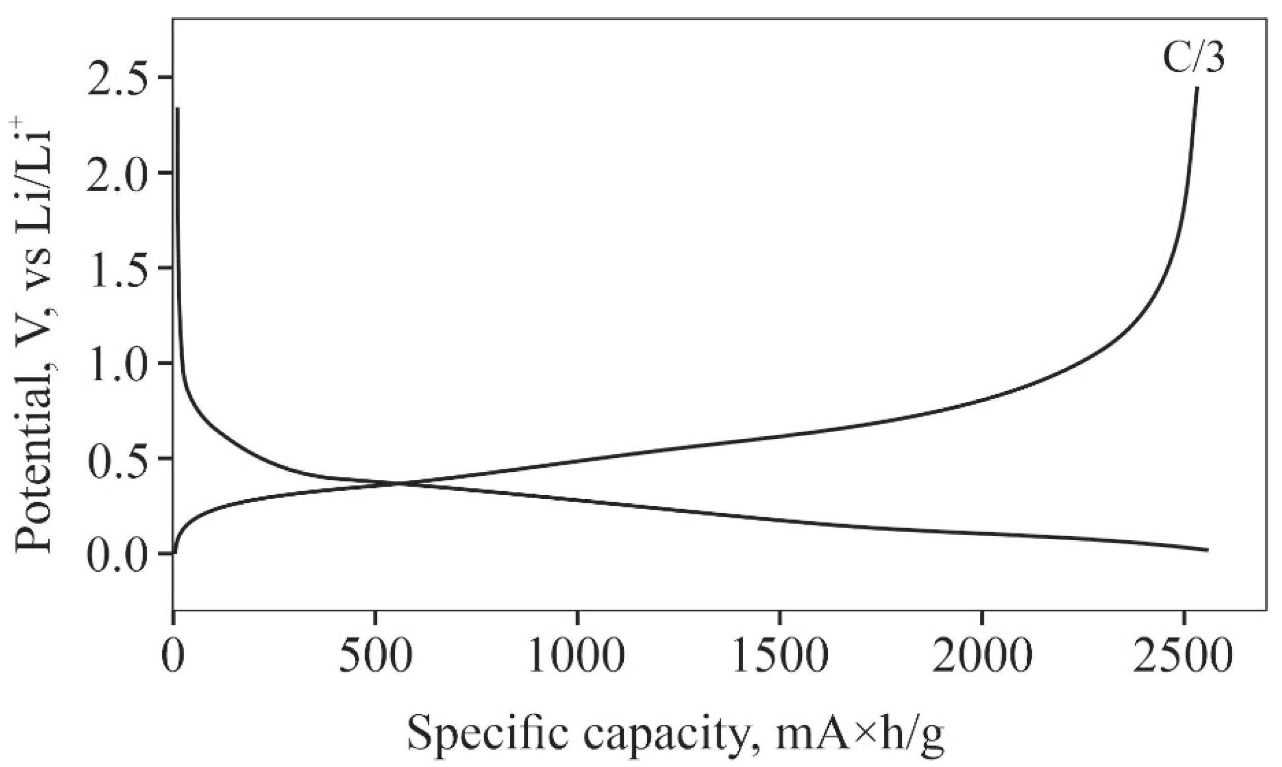
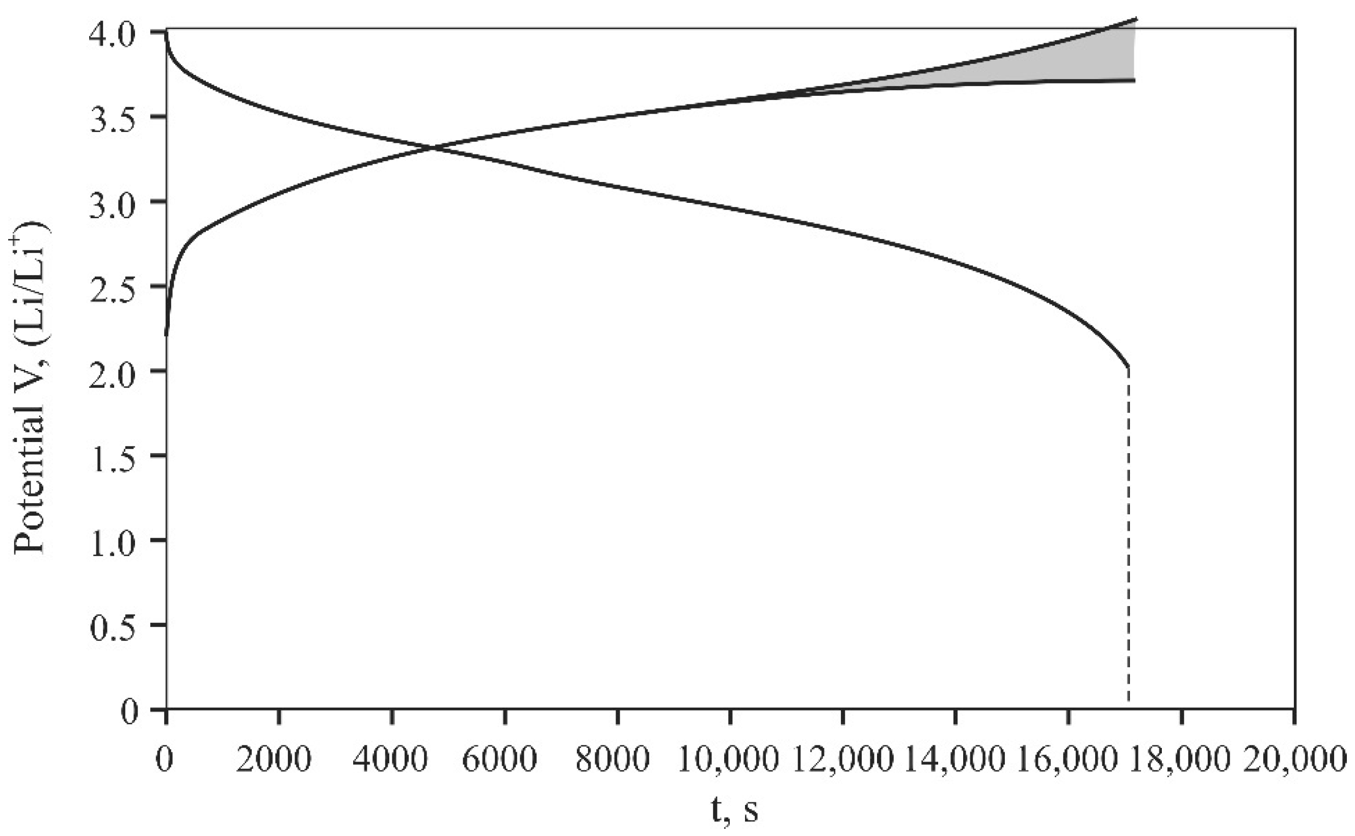
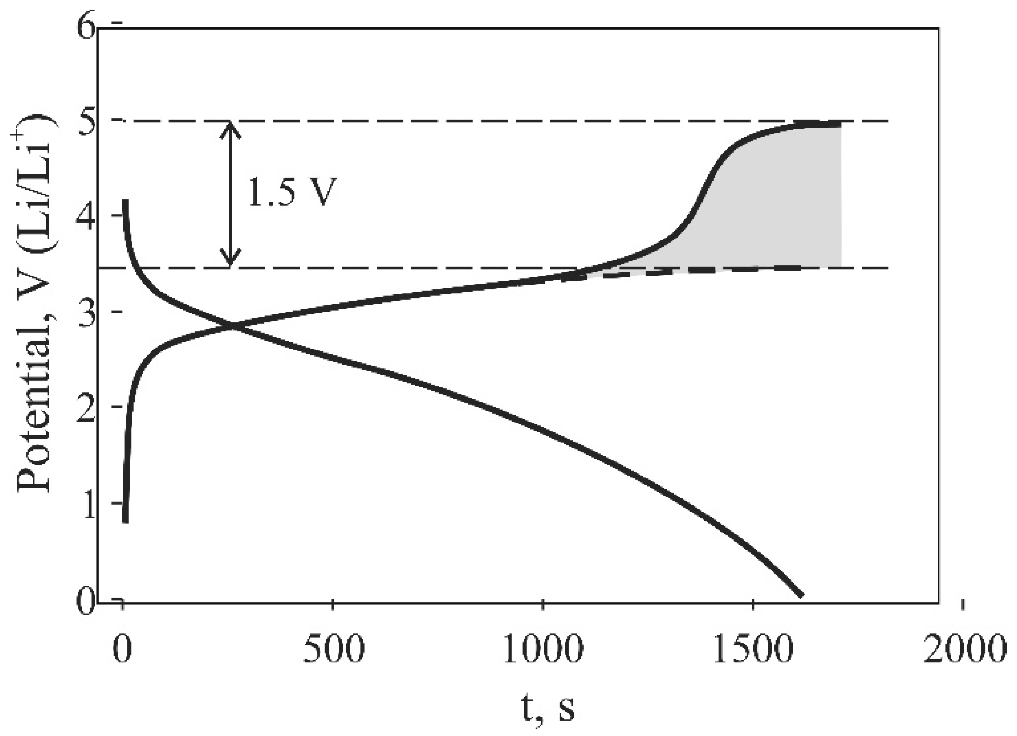
2.3. Features of Si@O@Al Electrodes Charging

The charge–discharge characteristics of the batteries were studied using the galvanostatic cycling method at various values of current and initial and final voltages. As a rule, the discharge current was equal to the charge current; in some experiments, these parameters were different. The studies were carried out using an automated charge–discharge complex AZRIVK-0.05 A-5 V (Booster, Saint Petersburg, Russia) and multichannel galvanostats-potentiostats P-20x8 and P-40x (Electrochemical Instruments, Chernogolovka, Russia). Figure 6 shows the charging and discharging curves of the T i | L i C o O 2 | L i P O N | S i @ O @ A l | T i battery in the settled mode (76th cycle) within the voltage range 0–4 V. The specific capacity of different batteries varied from 17 μA∙h/cm2 at a current of 3.5 μA/cm2 in a voltage window of 0.5–3.7 V up to 32.8 μA∙h/cm2 at a current of 7 μA/cm2 in a voltage window of 2.0–4.0 V. These data refer to the 30th test cycle.
A salient feature of the charging curve is a hike in a segment of 1100–1700 s (shaded area). Since the voltage window for lithium cobalt oxide batteries is limited to a value of 3.5 V, charging curves usually reveal only the beginning of the hike. Figure 6 shows the charging curve in a slightly wider voltage window of 0–4.2 V; therefore, the hike is more pronounced. Similar hikes were observed on the charge curves of the T i | L i V 2 O 5 | L i P O N | S i @ O @ A l | T i battery (Figure 7).

3. Discussion

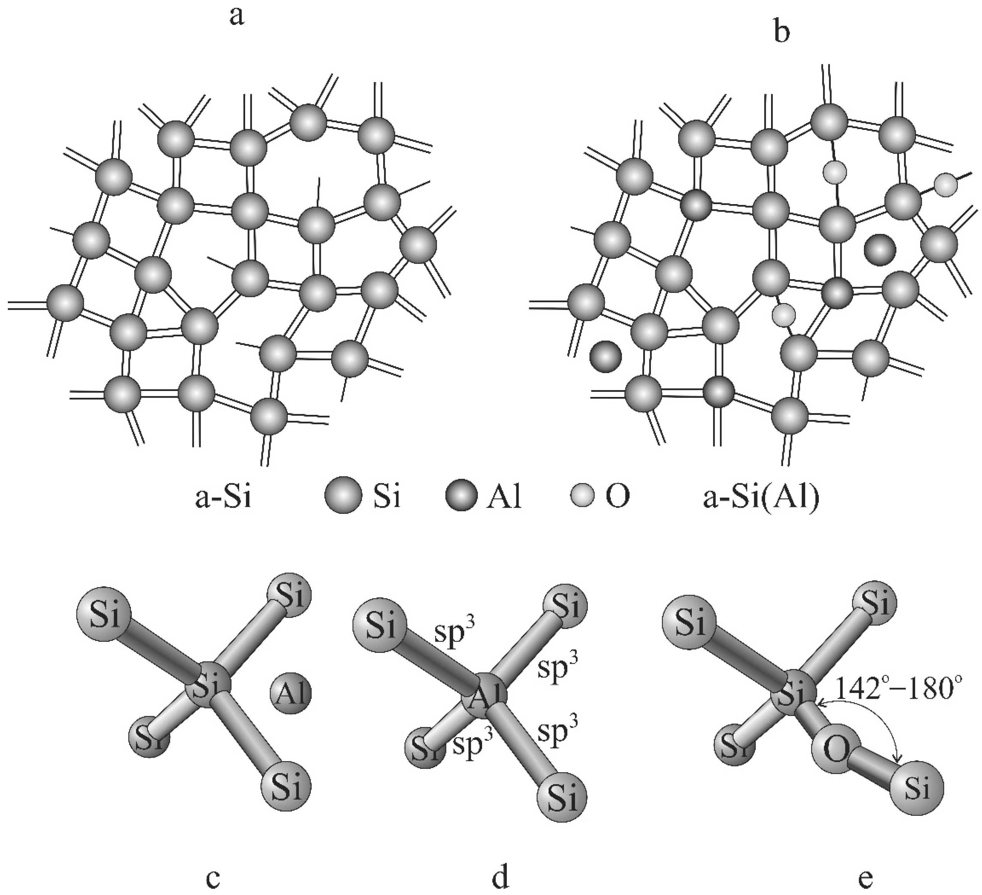
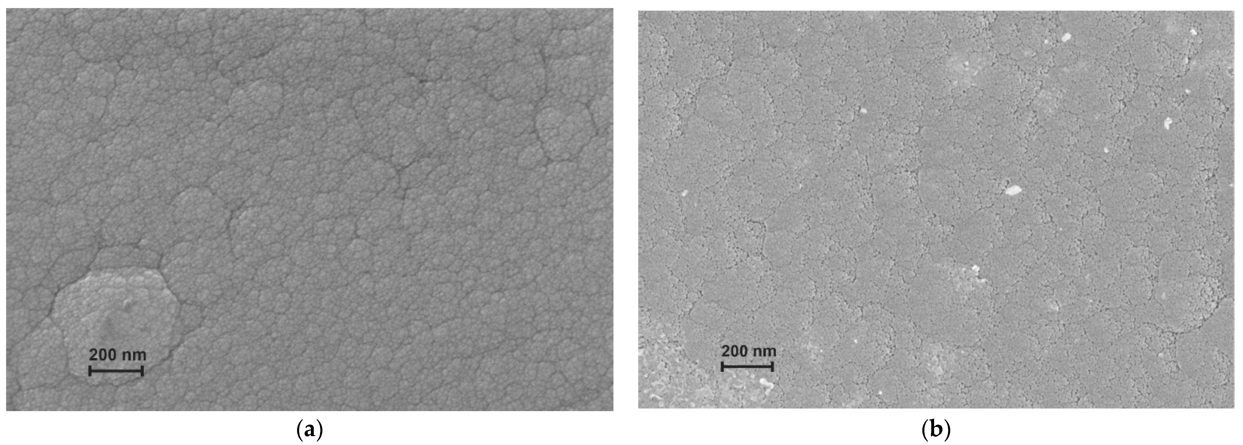
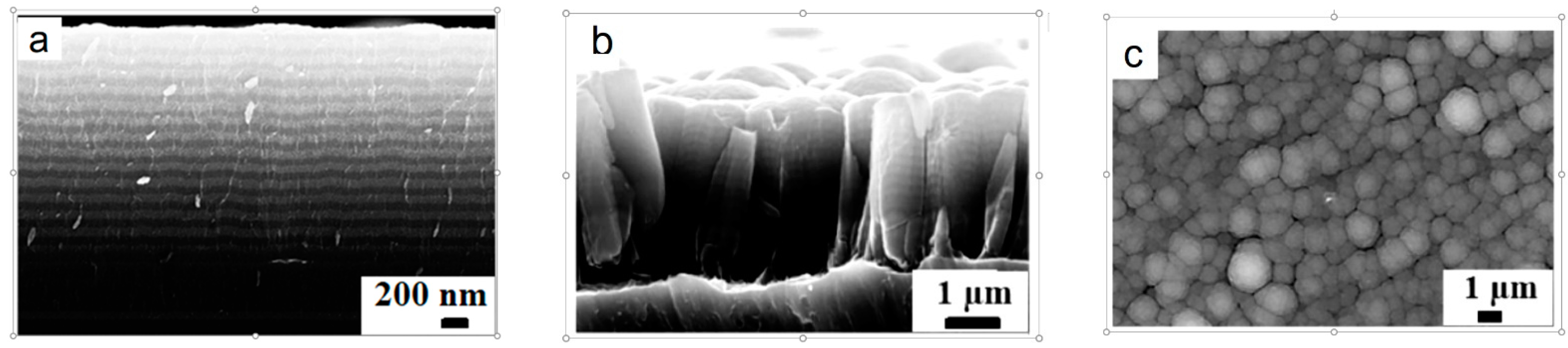
3.1. Structure and Electrical Properties of the Si@O@Al Nanocomposite

The hike formation on the charging curve is directly related to the structure and the elemental composition of the Si@O@Al nanocomposite, which consists of amorphous silicon (approximately 70%), oxygen (from 15% to 20%), and aluminum (from 10% to 15%, if the two targets, Si and Al, are sputtered). Unlike crystalline silicon, amorphous silicon can intercalate significantly more lithium without being destroyed [22,23,24]. If the density of crystalline silicon is 4.98 × 10 22   at . / cm 3 or 2.330   g / cm 3 , then amorphous silicon has a density of 4.90 × 10 22   at . / cm 3 or 2.285   g / cm 3 . It follows from a comparison of these parameters that the concentration of vacancies and voids in amorphous silicon is 8 × 10 20   a t . / c m 3 . Approximately the same values are given in [25]. Correspondingly, the same number of lithium atoms can be distributed in voids, practically without stresses in the lattice. This amount of lithium corresponds to the charge density 128   C / cm 3 = 35.6 × 10 3   A · h / cm 3 , which gives the specific capacity ~ 3.5   μ A · h / cm 2 at a Si@O@Al layer 1 µm thick. The actual capacity of individual SSLIB prototypes can be several times higher than this value.
It would seem that a-Si is ideal for making a negative electrode. However, this is not the case since the mobility of the charge carriers in amorphous silicon is very low and amounts to 2.0 × 10 8   m 2 ( V · s ) 1 at 300 K [26]. This value is comparable to the mobility of lithium ions in Si@O@Al 1.9 × 10 8   c m 2 / B · c [15], while for the normal operation of the electrode the mobility of the electrons or holes must exceed the mobility of lithium by orders of magnitude. The low mobility of the charge carriers in a-Si is due to the high concentration of structural defects and dangling bonds of silicon atoms. In terms of the band structure, this means a high density of states with a limited range of motion, which can capture electrons. Therefore, to obtain an electrode material with high conductivity, it is necessary to increase the concentration of charge carriers and passivate the dangling bonds. This is achieved by introducing additives of aluminum and oxygen.
During the electrode deposition by S i 0.9 A l 0.1 sputtering in an oxygen flow, silicon, aluminum, and oxygen mixes at the atomic level, and upon deposition, form the Si@O@Al nanocomposite (Figure 8b). The conductive basis of the nanocomposite is the a-Si(Al) solid solution, where Si is the solvent and Al is the solute. The concentration of the majority carriers (holes) depends on how the Al is introduced into the crystal lattice of amorphous silicon. The possible ways of introducing Al are shown in Figure 8. An Al atom can be located in voids or interstices of the crystal lattice without forming a chemical bond with silicon atoms (Figure 8c). In this case, the holes’ concentration does not change. In the second case, the Al atom passes from the ground state 3 s 3 p to an excited state 3 s 3 p , and capturing one more electron to the p-orbital from the neighboring silicon atom, forms an sp3-hybridized state (Figure 8d). In this case, a hole is generated in the valence band. In the sp3-hybridized state, electron density clouds of Al are directed to the tetrahedral vertices, just as in silicon, which allows the Al atom to be embedded in the Si crystal lattice, forming a substitutional solid solution a-Si(Al). Thus, the admixture of aluminum makes it possible not only to increase but also to regulate the conductivity of the nanocomposite electrode. It is important to note that in the state of phase equilibrium, the solubility of aluminum in silicon is very low and its maximum value, according to various data, ranges from 0.016 at. % to 0.038 at.%. Obtaining a higher concentration of aluminum in a-Si(Al) is possible only by PVD deposition.
While the mechanism for increasing the hole concentration is clear and consists in doping a-Si with aluminum, the mechanism for reducing the density of localized states remains unclear. On the one hand, this can be the same doping process, which proceeds according to the type of the low-temperature annealing of the silicon defects with lithium [27]. This mechanism is quite possible because aluminum has a high diffusion coefficient in silicon 10 14   c m 2 · s 1 [28]. Here, it should be clarified that in [28] diffusivity values were obtained for a very low concentrations and gradients due to the low solubility of aluminum in silicon. If one allows for the annealing of defects with aluminum, then along with the hole concentration, the degree of amorphous silicon ordering, and possibly the fraction of nanocrystalline silicon, should also increase. On the other hand, dangling bonds can be passivated by the so-called bridging oxygen (Figure 8e). Indeed, the length of the siloxane chain Si–O–Si is 3.28 Å, while the length of the Si–Si bond is 3.24 Å, which makes it possible to form Si–O–Si at the site of the defect. In this case, the angle between the bonds is 142.5° [29], i.e., the structural defect itself during the formation of the siloxane bond may be preserved. In other words, the passivation of dangling bonds with oxygen does not always lead to structure ordering, as in the case of aluminum. Another option for the passivation of dangling bonds can be the formation of molecular clusters (MC) of SiO2, which is more likely, given the high oxygen concentration of 15–20%. At the same time, MC SiO2, embedded in the a-Si(Al), disperses amorphous silicon, forming a percolation cluster. This is indicated by the varistor effect, which is clearly manifested when measuring the current-voltage (I–V) characteristics of Si@O@Al.
The assumption that the SiO2 domains do not reach the size of a nanoparticle, but most likely form an MC, is confirmed by the results of [30]. In this work, Si@O@Al films subjected to etching in a H F : N H 4 F : H 2 O solution were studied. The etching time of the films ranged from 5 to 30 min. The experimental samples treated in this way were studied by scanning electron microscopy (SEM) and energy dispersive microanalysis using a Supra 40 scanning electron microscope (Carl Zeiss, Oberkochen, Germany). The film surfaces before and after half an hour of etching are shown in Figure 9. In the presented images, there are no noticeable changes in the structure or the pores’ size caused by the etching. It should be clarified that Figure 9 shows different sections of the film, because the areas exposed to the electron beam were etched faster than the neighboring areas, so their repeated study by the SEM method gave a distorted idea of the surface modification by etching. An analysis of the elemental composition by the energy dispersive analysis, performed on a Supra 40 INCAx-act SEM attachment (Oxford Instruments, Yatton, UK), also did not reveal any change in the oxygen content. The oxygen concentration values were randomly distributed and belonged to the interval from 10.12 at.% to 10.85 at.%. However, the charge–discharge characteristics of the etched films differed markedly from the initial ones. They had a high specific capacity and withstood charge–discharge activity in a liquid electrolyte in the 10C mode for several cycles, after which they restored their characteristics. At the same time, these films were not very stable and degraded after 30–40 charge–discharge cycles. All of the above suggests that it is most likely that the oxygen atoms are distributed over the volume of the Si@O@Al nanocomposite in the form of MCs. When a film is etched in a solution of hydrofluoric acid and ammonium fluoride, only an insignificant part of the MC located on the pore surface is etched, which leads to an increase in the diffusion coefficient of lithium. These molecular clusters play a very important role in lithium transport, as they increase the area of grain boundaries along which lithium diffusion occurs. In the Si@O@Al nanocomposite, the diffusion coefficient of lithium amounts to 5 · 10 10   c m 2 s 1 [15].

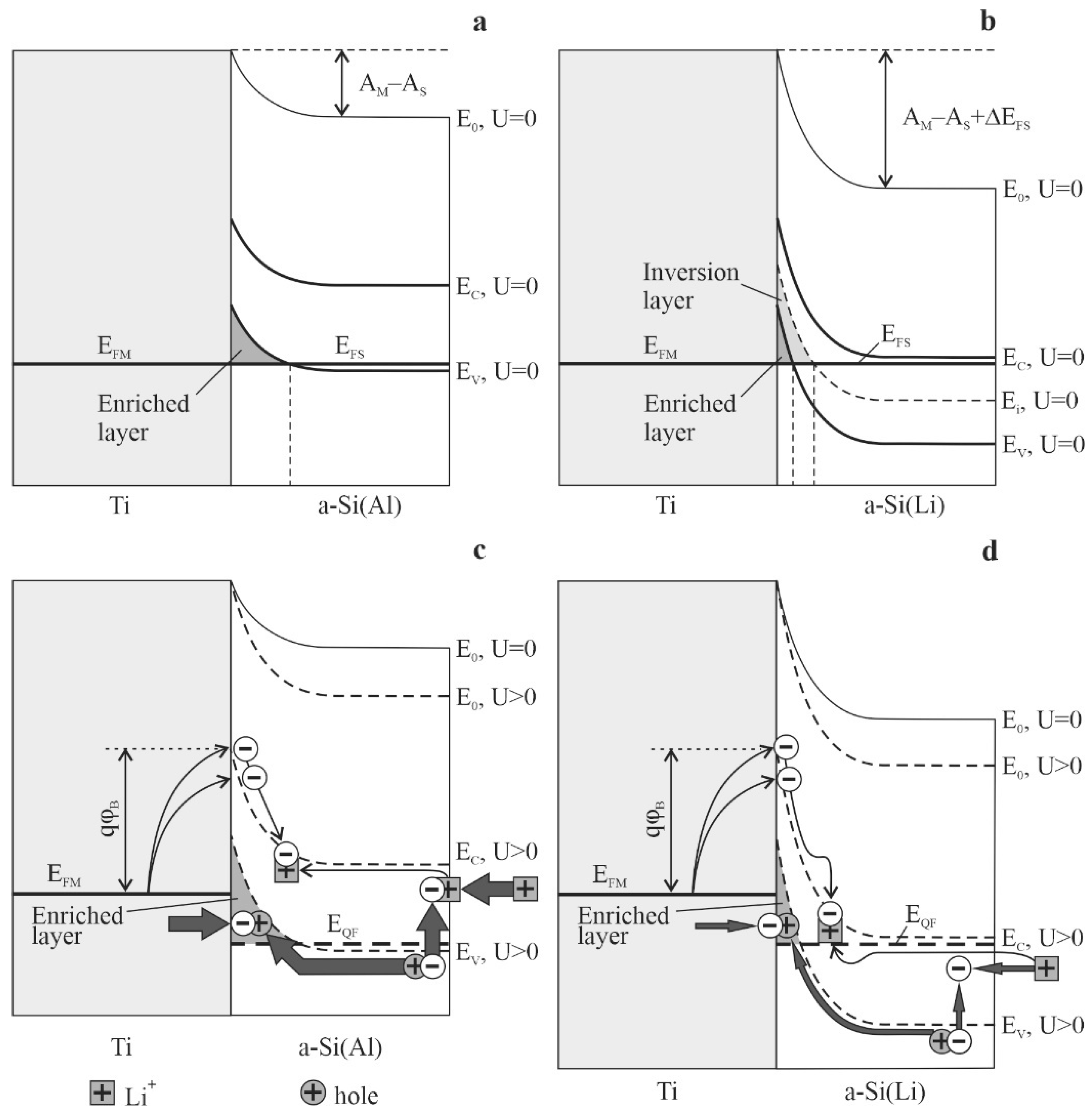
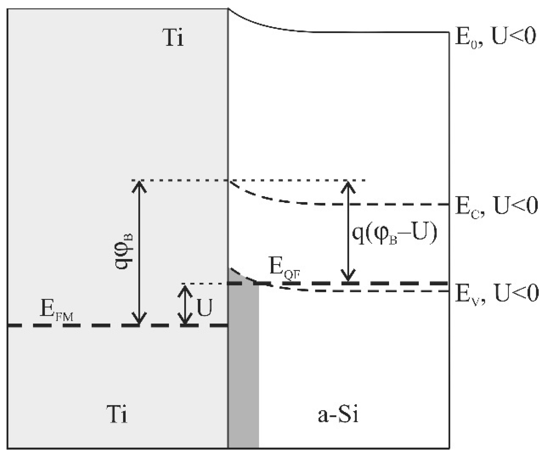
3.2. Model of Hike Formation during Lithiation of the Si@O@Al Electrode

At a qualitative level, the explanation of the potential hike at the charging curve upon lithiation of the Si@O@Al nanocomposite is as follows [31]. At a low lithium concentration, the solid solution α-Si(Al), which forms the conductive basis of the Si@O@Al nanocomposite, is a p-type semiconductor, and its contact with Ti is an ohmic one. The band structure of the Ti|α-Si(Al) junction at zero bias is shown in Figure 10a. The Fermi level in the a-Si(Al) system is settled near the hole mobility threshold EV. At a high lithium concentration, the α-Si(Al) transforms into α-Si(Li), where the symbols in parentheses denote the main dopant. Lithium atoms passivate the remaining dangling bonds, due to which the density of the localized states decreases, and the Fermi level moves to the electron mobility threshold EC. Accordingly, the zones in the volume move down relative to EFM by an amount of Δ E F S (Figure 10b). To the left of the point of Ei’s (the Fermi level of intrinsic semiconductor) intersection with the actual Fermi level, an inverse layer is formed, and to the left of the point of the intersection of EV with the EFS an enriched layer of holes appears.
When charging (Figure 10c), the junction is biased in the forward direction (i.e. when the minus is applied to the titanium), so the bands in the bulk of the semiconductor and the quasi-Fermi level in Figure 10c moves lower compared to Figure 10a. When charging, two types of charge carriers flow to Ti from the a-Si(Al) side: holes and lithium atoms. Figure 10c shows that most of the lithium ions are reduced near the Si@O@Al|LiPON interface, and a hole in the valence band is generated. Further, lithium atoms move deep into the negative electrode due to diffusion, while the electric current is created by holes that recombine with electrons at the interface with Ti, i.e. at the initial stage of charging, the current in the Si@O@Al electrode is the so-called recombination current. The electrons crossing the boundary from the side of the metal can be conditionally divided into two streams: electrons whose energy satisfies the condition ε E F M q φ B , and electrons with energy ε E V . The first flow is depicted in Figure 10c with a thin arrow, since the Schottky barrier has been overcome by electrons from the tail of the Fermi–Dirac distribution (this also includes electrons that overcome the barrier by tunneling). The value of this current is several orders of magnitude smaller than the recombination current, which is depicted by wide arrows.
As the lithium concentration increases, the acceptor impurity Al is compensated by the donor impurity Li, the Fermi level of the semiconductor rises to the electron mobility threshold EC, and the band structure acquires the form shown in Figure 10d. Now, the electrons become the majority carriers, and the Ti|a-Si(Li)) junction is consequently reverse-biased. In this case, the above-barrier and tunnel currents of the electrons from the metal do not undergo significant changes, so their value remains limited by the saturation current. At the same time, the hole current decreases significantly due to a decrease in the hole concentration and a decrease in the thickness of the enriched layer. Naturally, the resistance Ti|Si@O@Al junction raises relative to its value at the beginning of the charging, and to maintain the given galvanostatic mode, the galvanostat raises the voltage. This increase in voltage appears as a spike in the charging curve.

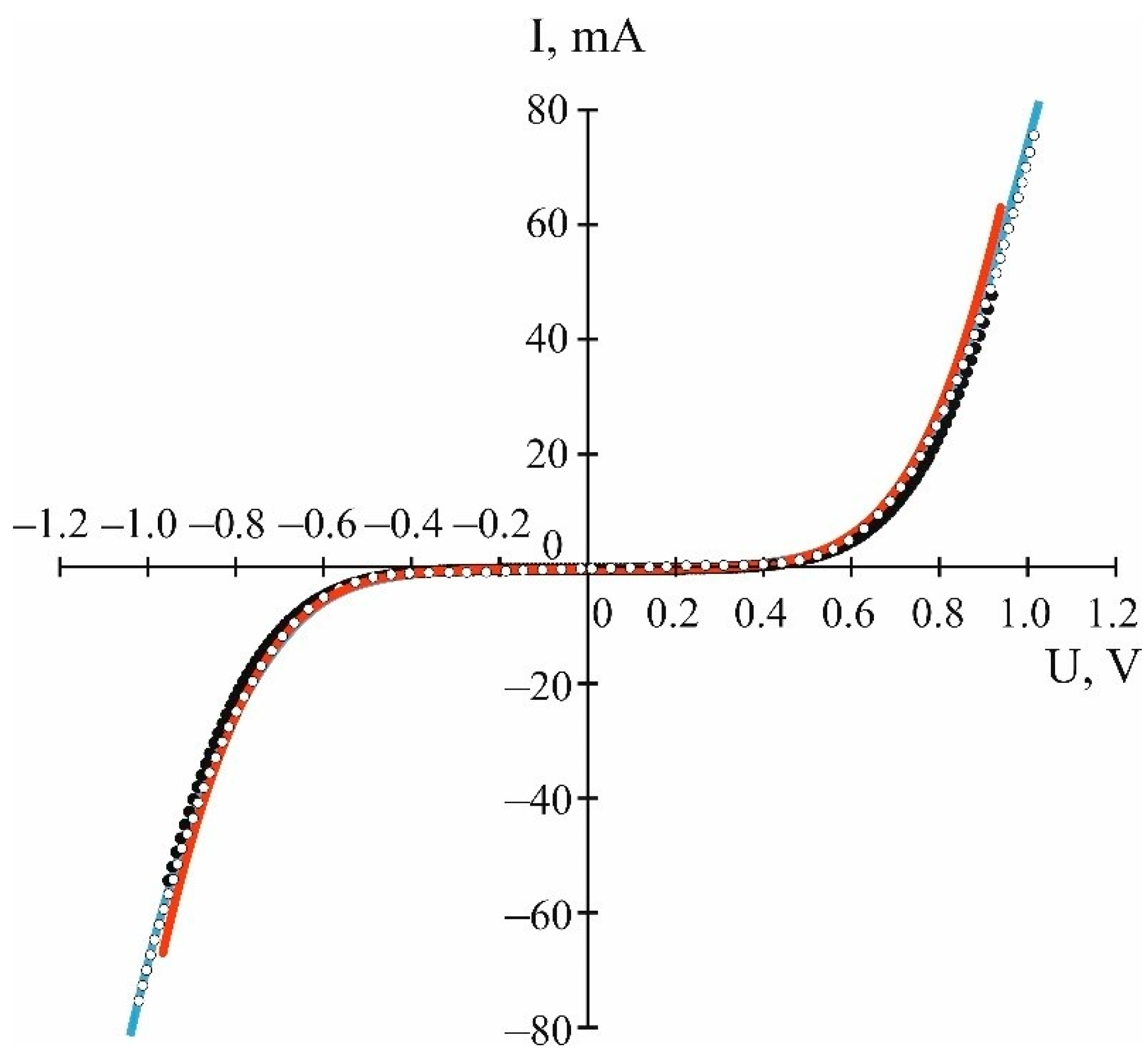
3.3. Experimental Confirmation of the Hole Conductivity of Si@O@Al

To experimentally confirm the hole conductivity of the a-Si(Al) solid solution, test structures Ti (200 nm)|Si@O@Al (180 nm)|Ti (200 nm) with an area of 1 × 1 cm2 were fabricated. In these structures, the Si@O@Al nanocomposite does not contain Li, while the concentration of the Al acceptor impurity is high enough to provide the noticeable holes’ concentration if it is really an a-Si(Al) substitutional solid solution. The I–V characteristics of the metal–semiconductor transition can serve as the confirmation of p-type conductivity. Since the work function of Ti is greater than the work function of a-Si(Al), the metal–semiconductor junction for an n-type semiconductor must be rectifying, and for a p-type it must be ohmic. In the first case, the current through the structure quickly reaches the saturation (~10−10 A) and does not depend on voltage until breakdown occurs. In the case of an ohmic contact, the forward branch of I–V must be linear and the reverse one should be exponential. That is to say, the test structure Ti|Si@O@Al|Ti consists of two Schottky diodes with a common anode. Accordingly, only the reverse branch will always be visible from the I–V characteristics of such a structure, since the resistance in the forward direction is sufficiently small. The reverse current is created by minority charge carriers that overcome the Schottky barrier, the height of which depends on the bias voltage U. This process is explained by the band structure of the a-Si(Al)|Ti junction shown in Figure 11.
With a reverse bias (a plus on a metal), the current through the junction in a p-type semiconductor is created by minority charge carrier-electrons. The total current density is the sum of the thermionic emission currents from metal to semiconductor and from semiconductor to metal. In the first case, electrons overcome the potential barrier q φ B ; in the second case, q ( φ B U ) , where φ B is the height of the Schottky barrier, and U is the bias voltage across the entire structure. Thus, the resulting electron current is directed from the semiconductor to the metal, and its density is as follows
I = I S ( e q ( U U V ) k B T 1 ) ,
where I S = λ R A 0 T 2 e q φ B k B T is the saturation current density; λR is a material-specific correction factor; A0 is the universal constant (Richardson constant); kB is the Boltzmann constant; T is the absolute temperature; q φ B is the height of the Schottky barrier; U is the bias voltage. Equation (1) takes into account that the voltage at the junction is less than the bias U by the value of the voltage drop in the nanocomposite layer. The I–V characteristics of the Ti|Si@O@Al|Ti test structures (Figure 12) were recorded by cyclic voltammetry at a scanning rate of 1 mV/s (red line), 5 mV/s (blue line), and 10 mV/s (black circles). Since the graph is clearly nonlinear, it can be assumed that the Si@O@Al nanocomposite features a varistor effect, which occurs quite often in nanocomposite materials. In most cases, the resistance of nonlinear materials is satisfactorily described by the expression
U V = I α + R 0 I ,
where is the coefficient of dimension Ω · A 1 α [32], R0 is the residual resistance, and α is the reciprocal of the I–V nonlinearity coefficient. If we neglect the term R 0 I due to its smallness, then expression (1) takes the form
I = I S ( e q ( U I α ) k B T 1 )
Figure 12 shows the dependency graph (3) (empty circles) for the following values I S = 10 10   A · cm 2 ; = 1.56   Ω · A 1 α ; α = 0.45 . Relation (3) satisfactorily describes the experimental curves in the specified voltage range, from which it follows that the unlithiated Si@O@Al has a p-type conductivity and is a nonlinear material.
Expression (2) makes it possible to estimate the minimum value of the Si@O@Al resistance in the range 0 ÷ 0.08   A . Up to a small unknown constant R0 for = 1.56   Ω · A 1 α and α = 0.45 , relation (2) yields R = 6.26   Ω or σ = 2.86   ×   10 4   S · m 1 . This result agrees with the experimental data of [33] and several other works; therefore, at first glance, the aluminum impurity does not make a significant contribution to the hole conductivity. However, it should be borne in mind that the obtained conductivity value refers to a percolation cluster formed by a-Si(Al) nanoparticles, which play the role of a filler, separated by SiO2 MCs, which play the role of a dispersant. The resistance of homogeneous a-Si(Al) can be an order of magnitude lower.
Another important transition parameter is the height of the Schottky Barrier, which can be expressed in terms of the saturation current as
q φ B = ln ( A T 2 / I S ) k B T .
In the case under consideration, relation (4) yields q φ B = 1.24   eV . The height of the Schottky barrier in an ideal structure is defined as the difference between the work function of the metal and the electronic affinity of the semiconductor
φ B = ( A M χ ) / q .
This ratio allows one to find the electron affinity of amorphous silicon. However, it should be kept in mind that in a real structure the barrier height is always lower due to mirror charges, surface states, an electric double layer, and other reasons. Therefore, the electron affinity, determined from the ratio χ = A M q φ B and expressed in electron volts, will always be greater than the true value. In this case, the electron affinity of amorphous silicon is χ = 3.06   e V . In fact, this value may be even lower.

4. Conclusions

Until now, the main disadvantages of silicon were considered to be the high density of its crystal lattice, which leads to the destruction of silicon when a large amount of lithium is introduced, and the high binding energy of lithium on the surface, which prevents its diffusion deep into the crystal. As shown in the present work, these shortcomings can be overcome by disordering the silicon structure and its partial oxidation. Silicon amorphization makes it possible to reduce the mechanical stresses and increase the diffusion coefficient of lithium. Oxidation reduces the number of dangling bonds, while maintaining the amorphous structure and increasing the grain boundaries area. In addition, aluminum—being an acceptor impurity—increases the hole conductivity of silicon, which improves its discharge capacity and enables an increase in the charging current. Further improvement in amorphous silicon’s conductivity may occur after the first lithiation cycles due to the passivation of the remaining dangling bonds. Thus, silicon becomes not only a promising but also a realized material for the development of negative electrodes.
However, at the same time, silicon must satisfy one essential requirement: it must be a hole semiconductor with a high concentration of charge carriers. Since the work function of all metals used as current collectors is greater than the work function of silicon, the metal–semiconductor junction will be ohmic only for a hole semiconductor. Otherwise, a depletion layer in the contact area will limit the charging current up to the saturation current value. A high concentration of holes is necessary in order to maximally raise the lithium concentration threshold, beyond which the hole semiconductor becomes an intrinsic semiconductor, since after this threshold the metal–semiconductor contact becomes rectifying and reverse-biased. It remains forward-biased only for minority charge carriers, which maintain the charging current when silicon becomes first intrinsic and then electronic semiconductor. In the galvanostatic charge mode, the charger increases the voltage on the battery to maintain the current, which manifests itself in the form of a hike on the charging curve.
It should be clarified that the increases in the charging curves of the Si@O@Al electrodes in a liquid electrolyte (Figure 3) and within SSLIB (Figure 6 and Figure 7) have a different origin. In the first case, this is due to reaching the capacity limit, while in SSLIBs the increase in the charging curve is due to semiconductor compensation. This is confirmed by the values of the volumetric capacity corresponding to the beginning of the voltage growth on the charge curves (Table 4). It can be seen from these data that the lithium concentration when charging Si@O@Al in a liquid electrolyte is tens of times higher than when charging through LiPON. In other words, in a liquid electrolyte, when the type of electrode conductivity is changed, the resistance of the Ti-Si@O@Al transition does not change significantly. This is due to the deep penetration of the liquid electrolyte and the Faraday process acting on the downconductor, which shunts the Ti-Si@O@Al junction.
The above requirements for silicon-based electrodes have been met by a new nanocomposite material, Si@O@Al, obtained by the magnetron sputtering of silicon and aluminum in an oxygen flow. During the Si@O@Al deposition, a substitutional solid solution α-Si(Al) is formed, whose dangling bonds are passivated by oxygen. Due to this circumstance, the density of the localized states in the mobility gap is consequently significantly lower than in amorphous silicon. In this sense, Si@O@Al is similar to hydrogenated amorphous silicon. The main difference is that during the magnetron deposition of the nanocomposite, a significant part of Al participates in the formation of the silicon crystal lattice as a dissolved component, while the dangling bonds’ passivation is mainly due to oxygen. After the first cycles of lithiation, the so-called low-temperature annealing of the defects occurs, during which the remaining dangling silicon bonds are passivated. In addition, Si@O@Al is relatively easy to manufacture, and its elemental composition and specific capacity can be controlled over a wide range of values. It is significant that Si@O@Al has a high stability with respect to the reversible incorporation of lithium and can be stored in vivo for a long time (several years). Despite the difference in the thermal expansion coefficients, Si@O@Al demonstrates a good adhesion to the LiPON solid electrolyte and titanium current collector. These qualities of Si@O@Al enable its use for the fabrication of SSLIB, which was demonstrated in this work.

Author Contributions

A.S.R.—writing of original draft and methodology; A.A.M.—methodology and investigation; V.V.N.—investigation and visualization; S.V.K.—investigation and visualization; Y.S.E.—investigation; A.M.S.—conceptualization and supervision. All authors have read and agreed to the published version of the manuscript.

Funding

This research was funded by the Ministry of Science and Higher Education of the Russian Federation grant number 0856-2020-0006.

Institutional Review Board Statement

Not applicable.

Informed Consent Statement

Not applicable.

Data Availability Statement

Supporting reported results data can be found or get by demand at The Facilities Sharing Centre “Diagnostics of Micro- and Nanostructures” (FSC DMNS), P.G. Demidov Yaroslavl State University.

Conflicts of Interest

The authors declare that they have no conflict of interest. The funders had no role in the design of the study; in the collection, analyses, or interpretation of data; in the writing of the manuscript, or in the decision to publish the results.

References

  1. Skundin, A.; Kulova, T.; Rudy, A.; Mironenko, A. All Solid State Thin-Film Lithium-Ion Batteries: Materials, Technology, and Diagnostics, 1st ed.; CRC Press: Boca Raton, FL, USA; Taylor & Francis Group: Boca Raton, FL, USA, 2021; 214p, ISBN 9780367086824. [Google Scholar]
  2. Cymbet.com. Available online: https://www.cymbet.com/wp-content/uploads/2019/02/DS-72-41.pdf (accessed on 9 June 2022).
  3. Jones, S.D.; Akridge, J.R. Thin film rechargeable Li batteries. Solid State Ion. 1994, 69, 357–368. [Google Scholar] [CrossRef]
  4. Bates, J.B.; Dudney, N.J.; Neudecker, B.; Ueda, A.; Evans, C.D. Thin-film lithium and lithium-ion batteries. Solid State Ion. 2000, 135, 33–45. [Google Scholar] [CrossRef]
  5. Souquet, J.L.; Duclot, M. Thin film lithium batteries. Solid State Ion. 2002, 148, 375–379. [Google Scholar] [CrossRef]
  6. Patil, A.; Patil, V.; Shin, D.W.; Choi, J.-W.; Paik, D.-S.; Yoon, S.-J. Issue and challenges facing rechargeable thin film lithium batteries. Mater. Res. Bull. 2008, 43, 1913–1942. [Google Scholar] [CrossRef]
  7. Dudney, N. Thin film micro-batteries. Interface 2008, 3, 44–48. [Google Scholar] [CrossRef]
  8. Sun, C.; Liu, J.; Gong, Y.; Wilkinson, D.P.; Zhang, J. Recent advances in all-solid-state rechargeable lithium batteries. Nano Energy 2017, 33, 363–386. [Google Scholar] [CrossRef]
  9. Zhou, Y.N.; Xue, M.Z.; Fu, Z.-W. Nanostructured thin film electrodes for lithium storage and all-solid-state thin-film lithium batteries. J. Power Sources 2013, 234, 310–332. [Google Scholar] [CrossRef]
  10. Zuo, X.; Zhu, J.; Müller-Buschbaum, P.; Cheng, Y.-J. Silicon based lithium-ion battery anodes: A chronicle perspective review. Nano Energy 2017, 31, 113–143. [Google Scholar] [CrossRef]
  11. Feng, K.; Li, M.; Liu, W.; Kashkooli, A.G.; Xiao, X.; Cai, M.; Chen, Z. Silicon-based anodes for lithium-ion batteries: From fundamentals to practical applications. Small 2018, 14, 1702737. [Google Scholar] [CrossRef]
  12. Zhang, W.-J. A review of the electrochemical performance of alloy anodes for lithium-ion batteries. J. Power Sources 2011, 196, 13–24. [Google Scholar] [CrossRef]
  13. Szczech, J.R.; Jin, S. Nanostructured silicon for high capacity lithium battery anodes. Energy Environ. Sci. 2011, 4, 56–72. [Google Scholar] [CrossRef]
  14. Liang, B.; Liu, Y.; Xu, Y. Silicon-based materials as high capacity anodes for next generation lithium ion batteries. J. Power Sources 2014, 267, 469–490. [Google Scholar] [CrossRef]
  15. Kulova, T.L.; Skundin, A.M.; Andreev, V.N.; Gryzlov, D.Y.; Mironenko, A.A.; Rudyi, A.S.; Gusev, V.N.; Naumov, V.V. Cyclic Voltammetry Studies of Silicon–Aluminum Thin-Film Electrodes Synthesized in the Presence of Oxygen. Russ. J. Electrochem. 2015, 51, 1157–1161. [Google Scholar] [CrossRef]
  16. Kulova, T.L.; Mironenko, A.A.; Skundin, A.M.; Rudy, A.S.; Naumov, V.V.; Pukhov, D.E. Study of Silicon Composite for Negative Electrode of Lithium-Ion Battery. Intern. J. Electrochem. Sci. 2016, 11, 1370–1381. [Google Scholar]
  17. Airapetov, A.A.; Vasiliev, S.V.; Kulova, T.L.; Lebedev, M.E.; Metlitskaya, A.V.; Mironenko, A.A.; Nikol’skaya, N.F.; Odinokov, V.V.; Pavlov, G.Y.; Pukhov, D.E.; et al. Thin Film Negative Electrode Based on Silicon Composite or Lithium-Ion Batteries. Russ. Microelectron. 2016, 45, 285–291. [Google Scholar] [CrossRef]
  18. Mironenko, A.A.; Fedorov, I.S.; Rudy, A.S.; Andreev, V.N.; Gryzlov, D.Y.; Kulova, T.L.; Skundin, A.M. Charge–discharge performances of the Si–O–Al electrodes. Mon. Chem. Chem. Mon. 2019, 150, 1753–1759. [Google Scholar] [CrossRef]
  19. Ohara, S.; Junji Suzuki, J.; Kyoichi Sekine, K.; Takamura, T. A thin film silicon anode for Li-ion batteries having a very large specific capacity and long cycle life. J. Power Sources 2004, 136, 303–306. [Google Scholar] [CrossRef]
  20. Park, M.S.; Wang, G.X.; Liu, H.K.; Dou, S.X. Electrochemical properties of Si thin film prepared by pulsed laser deposition for lithium ion micro-batteries. Electrochim. Acta 2006, 51, 5246–5249. [Google Scholar] [CrossRef]
  21. Uehara, M.; Suzuki, J.; Tamura, K.; Sekine, K.; Takamura, T. Thick vacuum deposited silicon films suitable for the anode of Li-ion battery. J. Power Sources 2005, 146, 441–444. [Google Scholar] [CrossRef]
  22. Zhao, L.; Dvorak, D.J.; Obrovac, M.N. Layered amorphous silicon as negative electrodes in lithium-ion batteries. J. Power Sources 2016, 332, 290–298. [Google Scholar] [CrossRef]
  23. Reuter, F.; Baasner, A.; Pampel, J.; Piwko, M.; Dörfler, S.; Althues, H.; Kaskel, S. Importance of Capacity Balancing on The Electrochemical Performance of Li[Ni0.8Co0.1Mn0.1]O2 (NCM811)/Silicon Full Cells. J. Electrochem. Soc. 2019, 166, A3265–A3271. [Google Scholar] [CrossRef]
  24. Nitta, N.; Wu, F.; Tae Lee, J.; Yushin, G. Li-ion battery materials: Present and future. Mater. Today 2015, 18, 252–264. [Google Scholar] [CrossRef]
  25. Smets, A.H.M. Growth Related Material Properties of Hydrogenated Amorphous Silicon. Ph.D. Thesis, Technische Universiteit Eindhoven, Eindhoven, The Netherlands, 30 May 2002. [Google Scholar] [CrossRef]
  26. Moore, A.R. Electron and hole drift mobility in amorphous silicon. Appl. Phys. Lett. 1977, 31, 762. [Google Scholar] [CrossRef]
  27. Goldstein, B. Li-defect interactions in electron-irradiated n-type silicon by EPR measurements. Radiat. Eff. 1971, 8, 229–237. [Google Scholar] [CrossRef]
  28. Krause, O.; Ryssel, H.; Pichler, P. Determination of aluminum diffusion parameters in silicon. J. Appl. Phys. 2002, 91, 5645. [Google Scholar] [CrossRef]
  29. Steinfink, H.; Post, B.; Fankuchen, I. The Crystall Structure of Octamethyl Cyclotetrasiloxane. Acta Cryst. 1955, 8, 420–424. [Google Scholar] [CrossRef]
  30. Kulova, T.L.; Mazaletskii, L.A.; Mironenko, A.A.; Rudyi, A.S.; Skundin, A.M.; Tortseva, Y.S.; Fedorov, I.S. Experimental Study of the Influence of the Porosity of Thin-Film Silicon-Based Anodes on Their Charge-Discharge Characteristics. Russ. Microelectron. 2021, 50, 45–53. [Google Scholar] [CrossRef]
  31. Rudy, A.S.; Mironenko, A.A.; Naumov, V.V.; Churilov, A.B. Schottky Barrier in Si–M Structures of Solid-State Lithium-Ion batteries. Tech. Phys. Lett. 2022, 48, 32–35. [Google Scholar]
  32. Kerimov, M.K.; Kurbanov, M.A.; Sultanahmedova, I.S.; Faradzhzade, I.A.; Tatardar, F.N.; Aliyev, H.S.; Yahyaev, F.F.; Yusifova, U.V. Varistor effect in polymer-semiconductor composites. Semiconductors 2010, 44, 904–911. [Google Scholar] [CrossRef]
  33. Thomas, P.; Flachet, J. Conductivity measurements on UHV deposited amorphous silicon. J. Phys. Colloq. 1981, 42, C4-151–C4-154. [Google Scholar] [CrossRef]
Figure 1. Electron microscopic image of a cleavage (a,b) and surface (c) of a freshly made electrode with an Si@O@Al composite.
Batteries 08 00087 g001
Figure 2. X-ray diffraction pattern of a Si@O@Al film on a silicon substrate.
Batteries 08 00087 g002
Figure 3. Typical charging (cathodic) and discharge (anodic) curves of a Si@O@Al electrode with liquid electrolyte.
Batteries 08 00087 g003
Figure 4. Cross-section of a solid-state thin-film lithium-ion battery prototype.
Batteries 08 00087 g004
Figure 5. Mask device on a movable substrate holder: (a) as assembled for depositing the lower titanium layer (current-collector); (b) after deposition, the lower titanium current-collector and the lower electrode (electrode mask in photo is removed). 1 is rectangular silicon substrate with a layer of SiO2, 2 is copper mask with nine rectangular holes for deposition the lower titanium layer, 3 are guide pins, 4 is a copper frame for lateral fixation of the substrate, 5 are holes for guide pins, 6 is one of nine deposited rectangular bottom Ti contacts, and 7 is one of five deposited lower electrodes.
Batteries 08 00087 g005
Figure 6. Charge and discharge curves of the T i | L i C o O 2 | L i P O N | S i @ O @ A l | T i battery. Area S = 1.44 cm2; 31st cycle; voltage range 0–4.2 V; Current 10 μA. Specific capacity 32.8 μA∙h/cm2.
Batteries 08 00087 g006
Figure 7. Charge and discharge curves of the T i | V 2 O 5 | L i P O N | S i @ O @ A l | T i battery. Area S = 7.9 cm2; 119th cycle; voltage window 0–5 V; current 100 µA. Specific capacity 5.8 μA∙h/cm2.
Batteries 08 00087 g007
Figure 8. Two-dimensional models: a-amorphous silicon (a)-Si, (b)-Si@O@Al nanocomposite, (ce)-possible options of introducing aluminum into the amorphous silicon lattice (c,d), and dangling bonds passivation (e).
Batteries 08 00087 g008
Figure 9. Comparison of the surface morphology of Si@O@Al films: (a) original film; (b) after etching in solution H F : N H 4 F : H 2 O for 30 min.
Batteries 08 00087 g009
Figure 10. Band diagrams of the Ti|a-Si(Al) contact: (a) band structure of a-Si(Al); (b) band structure of a-Si(Li); (c) lowering of the a-Si(Al) zones at forward bias of the contact (plus by a-Si(Al)); (d) lowering of the a-Si(Li) zones at reverse bias of the contact (plus by a-Si(Li)); AM is the metal work function; EFM is the Fermi level of the metal, and EFS is the Fermi level of the semiconductor; EQF is the semiconductor quasi-Fermi level; E0 is the energy level of vacuum; Ec is the electron mobility threshold; EV is the hole mobility threshold, Ei is the Fermi level of intrinsic semiconductor; and U-contact is the bias voltage.
Batteries 08 00087 g010
Figure 11. Band structure of the reverse-biased Ti|a-Si(Al) transition. EFM is the Ti Fermi level; is the height of the Schottky barrier; U is the bias voltage; EQF is the quasi-Fermi level of a-Si(Al); EV is the holes’ mobility threshold; EC is the electrons’ mobility threshold; E0 is the vacuum level.
Batteries 08 00087 g011
Figure 12. The I–V characteristics of the Ti|Si@O@Al|Ti test structures: red line—scanning rate of 1 mV/s; blue line—5 mV/s; black circles—10 mV/s; empty circles—Equation (3).
Batteries 08 00087 g012
Table 1. Technological parameters for Si@O@Al electrodes magnetron deposition.
Cleaning and Deposition ParametersMVU TM Magna 10Oratorio 22
Cleaning
Ion source current, mA6363
Ar flow, sccm1515
Heating, °C200200
Heating time, s6060
Deposition
Pressure, Pa1.50.18
Ar flow, sccm4020
O2 flow, sccm0.70.6
Power, M1 * (Si0.9Al0.1), W600500
M2 * (Al) Power switching limits, Wmode 1
mode 2
200
50
-
Deposition time, min4516
* Magnetrons.
Table 2. Elemental composition (at.%) and thickness (μm) of the batch of homogeneous Si@O@Al films deposited on a silicon substrate.
Sample Nos.123456789101112131415
C3.183.123.183.483.143.532.823.031.641.210.581.42.421.562.41
O30.331.431.032.232.333.332.6113.312.312.516.422.322.915.2013.2
Al6.025.455.685.175.235.405.274.154.584.323.733.393.37.207.03
Si59.558.0357.1455.1554.3351.7752.3071.5272.4871.9768.2960.9158.3862.0462.36
Film thickness, μm0.810.800.860.750.640.690.631.811.761.782.002.352.601.901.90
Table 3. Parameters of targets and film deposition.
TargetMain Substance Content,%GasPressure, µbarMagnetron Power, WDeposition Rate, nm/minThickness, nm
Ti99.95Ar230020200 (bottom and top layers)
LiCoO299.920Ar + 5O2102004.5500
LixV2O599.910Ar + O22.22002.7500
Li3PO499.9N221505.6600−800
S i 0.9 A l 0.1 99.99200Ar + 0.6O217.540050200
Table 4. Volumetric capacity of Si@O@Al at the beginning of the voltage growth of the charge curves.
CapacitySi@O@Al in the Test CellSi@O@Al in SSLIB with LiCoO2 CathodeSi@O@Al in SSLIB with V2O5 Cathode
CV, A·h/cm350.110.058
CV, C/cm318,000396209
CLi, cm−311 × 1022 *0.25 × 10220.13 × 1022
* CSi = 5 × 1022 cm−3.
Publisher’s Note: MDPI stays neutral with regard to jurisdictional claims in published maps and institutional affiliations.

