Article

Assessment of Laser-Ablated Silicon Wafers as Lithium-Ion Battery Anodes

1
Department of Chemical Engineering, University of Virginia, 102 Engineers Way, Charlottesville, VA 22904, USA
2
Charles L. Brown Department of Electrical and Computer Engineering, University of Virginia, 351 McCormick Road, Charlottesville, VA 22904, USA
*
Author to whom correspondence should be addressed.
Batteries 2025, 11(4), 121; https://doi.org/10.3390/batteries11040121
Submission received: 24 February 2025 / Revised: 17 March 2025 / Accepted: 21 March 2025 / Published: 23 March 2025

Abstract

:
Silicon materials have been widely investigated as anode materials for lithium-ion batteries. However, they are typically processed as fine powders into composite electrodes. Towards potentially repurposing silicon wafers as battery anodes, in this work, the impacts of the laser ablation of silicon wafers on electrochemical cycling outcomes were investigated. Both pristine wafers and laser-ablated wafers were assessed, where the silicon anodes were paired with all-active material LiCoO2 cathodes to assess the system as lithium-ion full cells. The laser ablation process modified the surface morphology of the silicon wafers, creating a polycrystalline silicon layer with increased surface area. Electrochemical cycling revealed that the laser-treated wafers demonstrated higher capacity retention and improved rate capability compared to untreated wafers, especially when discharged at the highest current density of 7 mA cm−2. This work demonstrated the improvements in electrochemical outcomes with the direct use of silicon wafers as lithium-ion anodes when laser ablation surface treatment is applied.

1. Introduction

Devices, transit, and utilities powered by electricity have become prolific in our daily lives. As these applications have increasing scale, functionality, and complexity, their power requirements have risen significantly [1,2]. Consequently, the demand for improvements in power sources has also increased, spurring advancements in power generation, power efficiency, and energy storage technologies. While fossil fuel-based power generation remains dominant, global interest in sustainable energy solutions has surged, motivated by environmental concerns, resource depletion, and evolving societal priorities [3,4]. Among various sustainable power generation methods, solar energy, harnessed through photovoltaic (PV) systems, has emerged as a leading technology due to its scalability, eco-friendliness, cost, and capacity to reduce greenhouse gas emissions [5,6].
The rapid growth of the solar industry has led to the widespread deployment of PV systems globally. However, like all technology, these systems have a finite lifespan, raising concerns about the decommissioning and material fate of solar power facilities [7,8,9]. Solar panels, the primary component of these system, are a significant focus of recycling efforts due to their large volume and potentially valuable constituent materials [10,11]. A central component of solar panels is the solar cell, made of silicon wafers, which presents an opportunity for reuse as a silicon source in various applications. While silicon is extensively utilized across numerous industries, its potential as a high-performance battery electrode material has garnered increasing interest in recent years due to its exceptional energy storage properties [12,13,14].
Efforts to reuse silicon from end-of-life solar panels for battery applications have centered on two primary approaches. The first involves pulverizing silicon panels to produce nano-silicon powders for use as battery anodes [14,15,16]. Silicon possesses a theoretical capacity of approximately 4200 mAh g−1, which is significantly higher than that of graphite, the most commonly used lithium (Li)-ion conventional anode material [17,18]. This high capacity is attributed to a multi-step alloying reaction of Si with Li, forming lithium silicide (LixSi) [19,20]. However, silicon undergoes substantial volume expansion—up to 300%—during lithiation, leading to mechanical instability, cracking, and eventual degradation of the electrode [21,22,23]. Nano-silicon powders partially address these issues by reducing particle size and improving structural stability [24,25]. Several techniques have been applied to overcome the challenges of silicon nano power anodes by producing silicon nanocomposites tailored to improve conductivity and structural stability [26,27]. However, achieving high areal mass loading with nano-Si powders can be challenging, and is a critical factor for electrode design in batteries [28,29].
A second approach to using Si in battery anodes involves utilizing intact silicon wafers as battery electrodes with surface modifications to enhance their performance. As silicon wafers can have challenges of fracture due to mechanical stress during cycling and relatively low electronic conductivity, techniques such as chemical etching, electrochemical treatments, photoresist patterning, and laser treatment have been explored. These techniques modify the surface properties of silicon wafers, aiming to improve mechanical stability, surface reactivity, and Li+ transport [30,31,32,33,34]. Laser treatments have potential advantages in their ability to precisely generate structured surfaces, which, for appropriate electrode design and processing, can improve cycling stability [33,35]. Despite these advancements, challenges remain in leveraging the high specific capacity of silicon wafers, including pairing them with cathodes that possess matching areal capacities. Most studies have focused on half-cells where lithium metal was the anode. Even in cases where full-cell evaluations were conducted, they were often assessed using low current densities. In contrast, this study assessed silicon wafer electrodes under a range of current densities, providing a more realistic representation of practical battery current densities that are experienced within a full cell.
The capacity of silicon wafer electrodes can be regulated by controlling the extent of lithiation during the charge/discharge cycling protocol. The areal capacity can be very high depending on the thickness of the wafer, which results in high areal loading. The relatively high areal mass and gravimetric capacity of silicon wafers is a unique characteristic that makes them a promising candidate for achieving high areal capacity and energy density compared to Si or Si/C composite electrodes in Li-ion batteries [36,37]. However, a limitation in their implementation in cells can be the availability of a suitable cathode with sufficient areal capacities due to pairing with the large areal mass of Si that would be present in a wafer. Conventional cathodes using carbon additives and polymer binders face challenges in increasing areal loading to match the capacity of a silicon anode with even relatively low mass loading due to the high gravimetric capacity of Si materials. In our group, we have fabricated and reported all-active material (AAM) electrodes, composed entirely of electroactive material without carbon additives or binders [38,39]. AAM electrodes have achieved high areal capacity enabled by hydraulic compression and mild sintering, allowing customization of electrode thickness from tens of micrometers to millimeters [38,39,40]. This processing route and adaptable loading makes AAM electrodes well-suited for pairing with high capacity anodes, including silicon wafers. Additionally, the absence of inactive additives in the AAM electrode provides relative improvements in ionic transport properties within the electrode microstructure relative to conventional composite electrodes [40,41,42].
In this study, pristine and laser-ablated silicon wafers were prepared as Li-ion battery anodes and paired with AAM LiCoO2 (LCO) cathodes to fabricate and evaluate Si/LCO full cells. Laser ablation was used to create both single-sided and double-sided surface modifications on the silicon wafers. The electrochemical outcomes, including the rate capability of the resulting cells, were systematically evaluated to assess the impact of the surface treatments on battery cycling.
By pairing the Si wafer electrodes with AAM LCO cathodes, we successfully demonstrated reversible cycling of cells with areal capacities of 7 mAh cm−2. The processing method for the Si could be adapted to more directly use Si wafers from spent solar panels, taking advantage of a laser ablation process that has already been demonstrated for the selective removal of silver from the module’s wafers [43].

2. Materials and Methods

2.1. Silicon Wafer Electrode Preparation

Silicon wafers were used as anodes without any treatment, or after being textured using a laser ablation process. For wafers that were textured, a 355 nm wavelength nanosecond pulsed laser (Coherent Matrix 355-8-50, Saxonburg, PA, USA) was used to ablate the silicon wafer. The pulse width was 20 ns and, for this study, the laser was operated at 50 kHz pulse repetition rate with an average power of 8 W. High Dynamics PIMag linear XY stages (PI, Auburn, MA, USA) were used for mounting the samples, and the laser beam was scanned using a Sino-Galvo SG7210 system (Sino-Galvo, Zhenjiang, China) [44,45].
Pulsed UV light has short wavelengths (193–355 nm) with high absorption by silicon to enable precise energy deposition, reducing heat-affected zones and preventing thermal damage, which is critical for maintaining the wafer’s structural integrity. The laser beam was scanned on a wafer sample at a constant speed of 500 mm/s. Before laser ablation, the silicon wafers underwent a cleaning process using an ultrasonic cleaner with deionized (DI) water to remove surface contaminants, especially dust particles.

2.2. Cathode Preparation

The cathode paired with the Si anodes was an AAM LCO cathode [46,47,48]. The synthesis, preparation, and characterization of these materials can be found in previous reports [39,49]; however, short descriptions for the processing used in this particular work are provided. The initial synthesized precursor, which was converted to LCO, was cobalt oxalate dihydrate (CoC2O4·2H2O), which was made via a coprecipitation method. Cobalt sulfate heptahydrate (CoSO4·7H2O, Fisher Scientific, Hampton, NH, USA) and sodium oxalate (Na2C2O4, Fisher Chemical, Pittsburgh, PA, USA) were separately dissolved in 400 mL of DI water to achieve concentrations of 0.2 M for each. Each solution was separately stirred at 300 rpm and heated to 60 °C using hot plates. Upon reaching 60 °C, the cobalt sulfate solution was added to the sodium oxalate solution all at once. The resulting mixture was stirred continuously at 300 rpm and maintained at 60 °C for 30 min to complete the coprecipitation reaction. The precipitate formed was collected via filtration, washed thoroughly with 1600 mL of DI water to remove residual impurities, and then dried overnight at 80 °C in a drying oven. The dried cobalt oxalate powder was then combined with lithium carbonate (Li2CO3, Fisher Scientific, Hampton, NH, USA) at a Li:Co molar ratio of 1.05:1, and the powder was blended by hand using a mortar and pestle until it appeared homogeneous to the naked eye. The resulting powder mixture was subjected to calcination in a box furnace under an air atmosphere. The calcination process involved heating the mixture at a rate of 1 °C min−1 to a temperature of 800 °C, followed by natural cooling to room temperature without a dwell period at the peak temperature or active control of the cooling rate. The calcined product was subsequently ground again with a mortar and pestle by hand to break up larger aggregates and achieve a fine, uniform powder.
To fabricate high-energy cathodes that more than balanced the high targeted areal capacity for the silicon wafer anodes, cathodes composed entirely of LCO electroactive material (and pores) with a relatively high areal weight loading were prepared. To improve loading outcomes, and facilitate the formation of high-loading LCO electrodes during hydraulic compression, the active material powders were coated with polyvinyl butyral (PVB, Pfaltz & Bauer, Waterbury, CT, USA), a sacrificial binder. Specifically, 0.5 mL of a 4.0 wt.% PVB solution in ethanol was blended with 1.0 g of LCO powder using a mortar and pestle until the solvent evaporated. The PVB-coated LCO powder was then pressed into 13 mm diameter pellets using a die within a hydraulic press (Carver, Wabash, IN, USA) at a pressure of 3000 psi for 10 s. The fabricated LCO pellets were targeted to achieve an areal capacity of 11 mAh cm−2, ensuring that the cathode provided at least 1.5 times the excess capacity relative to the capacity of the Si wafer anodes (set by capacity limits during electrochemical evaluation). This deliberate excess capacity for the LCO was intended to ensure multiple charge/discharge cycles could be achieved by providing additional Li available in the cathode to compensate for known capacity loss commonly reported for Si anode materials during electrochemical cycling [50,51].

2.3. Cell Fabrication

For cell assembly, LCO pellets were attached to stainless steel spacer disks with a diameter of 15.5 mm and a thickness of 0.5 mm using a carbon-based conductive paste. The paste was prepared by mixing 0.25 g of Super P carbon black with 5.0 g of a 5.0 wt.% polyvinylpyrrolidone (PVP, (C6H9NO)n, Sigma, St. Louis, MO, USA) solution in ethanol at 2000 rpm for 4 min, achieving a 1:1 weight ratio of conductive material to binder.
Si wafer electrodes and the attached LCO electrodes were dried at 80 °C in a vacuum oven to remove any residual moisture and ethanol. To prevent short circuits in these cells with relatively thick electrodes (compared to more conventional Li-ion cells) [52,53], two sheets of 25 µm thick microporous separators (Celgard 2325, Celgard, Charlotte, NC, USA) were placed between the cathode and anode. The separators were punched into circular discs with diameters of 18 mm to match the interior dimensions of the 2032-type coin cell. The electrolyte used for cell assembly consisted of 1.2 mol L−1 lithium hexafluorophosphate (LiPF6) dissolved in a solvent mixture of ethylene carbonate and ethyl methyl carbonate in a 3:7 weight ratio (Gotion, Fremont, CA, USA). The 2032-type coin cells were assembled in an argon-filled glovebox to minimize contamination from moisture or oxygen. The glovebox atmosphere was maintained to achieve oxygen and moisture levels below 1.0 ppm. Figure 1 shows schematic cartoons of Si wafer electrodes used in this study and the configuration of the full cells.

2.4. Characterization of Silicon Wafer Electrode

The structure of the silicon wafer electrode was analyzed using X-ray diffraction (XRD). Measurements were performed with a Malvern-Panalytical Empyrean X-ray diffractometer (Malvern, UK) equipped with a Cu Kα radiation source (λ = 1.54 Å). Scans were conducted over a 2θ range of 10° to 70°, with the resulting XRD patterns collected to identify crystallographic phases of silicon wafers following laser microtexturing.
The surface morphology and microstructure of the silicon wafer electrode were examined using FEI Quanta 650 scanning electron microscopy (SEM, Hillsboro, OR, USA). SEM imaging was performed under high-vacuum conditions at an accelerating voltage of 10 kV.
The laser-ablated pattern of the silicon wafer electrode was examined using an optical microscope (BX51M, Olympus Corporation, Tokyo, Japan) in reflection mode, equipped with a UC50 camera (Olympus Corporation, Tokyo, Japan).

2.5. Electrochemical Evaluation

The electrochemical properties of fabricated cells with a Si wafer anode and LCO cathode (Si/LCO full cell) were assessed using electrochemical charge/discharge cycling with constant current density for each half cycle (i.e., galvanostatic). Initially, the cell was cycled at a relatively low current density of 0.28 mA cm−2 for 10 charge and discharge cycles using a constant current charge–discharge method. To control the total cell capacity, the cycling procedure was set to limit the charge cycle to complete either when the potential reached a charge cutoff of 4.2 V (cell), or when the charge capacity achieved 7.0 mAh cm−2. Similarly, during discharge, the discharge cycle concluded when either the cell reached the lower voltage cutoff of 2.7 V, or when the discharge capacity of 7.0 mAh cm−2 was achieved. All charge cycles were concluded by reaching the capacity cutoff, while most discharge cycles were concluded by reaching the voltage cutoff.
After completing 10 cycles at the low current density, the rate capability of a cell was evaluated. For rate capability, the discharge process was conducted at increasing current densities of 0.35, 0.7, 1.4, 3.5, and 7.0 mA cm−2, with each discharge current used for 5 consecutive cycles. During these rate capability experiments, the charge current density was maintained at a constant 0.28 mA cm−2. Consistent with the initial cycling tests, the charge and discharge capacities were restricted to no more than 7.0 mAh cm−2 per cycle. Specifically, the charging process transitioned to the discharge process when the potential reached 4.2 V or when a capacity of 7.0 mAh cm−2 was achieved. Likewise, the discharge process switched back to the charging process when the potential dropped to 2.7 V or when the same capacity of 7.0 mAh cm−2 was discharged. All charge cycles were concluded by reaching the capacity cutoff, while most discharge cycles were concluded by reaching the voltage cutoff.
Electrochemical Impedance Spectroscopy (EIS) measurements were also conducted on cells at two stages: before cycling (fresh cell), after initial 10 cycles.

3. Results and Discussion

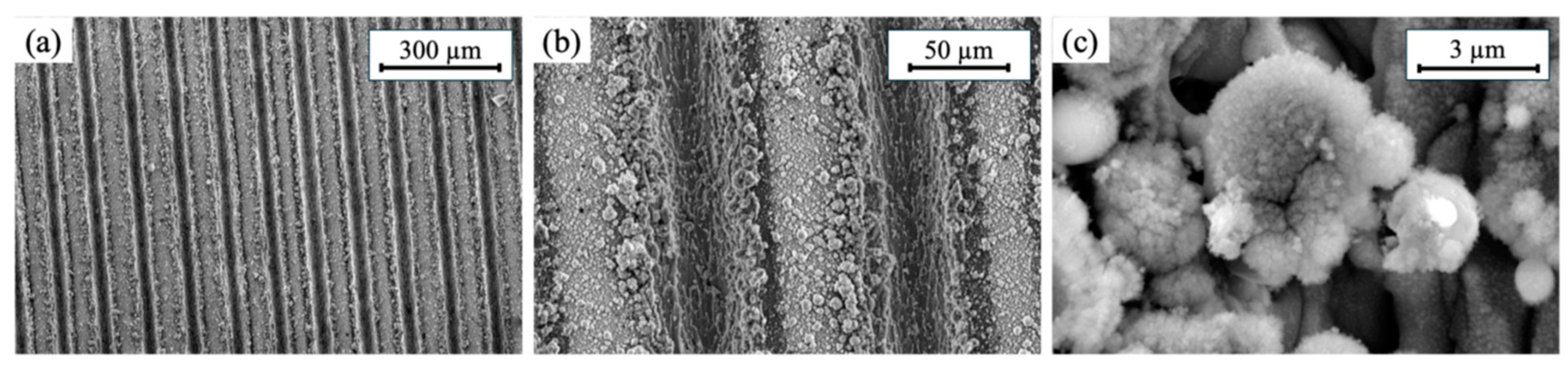
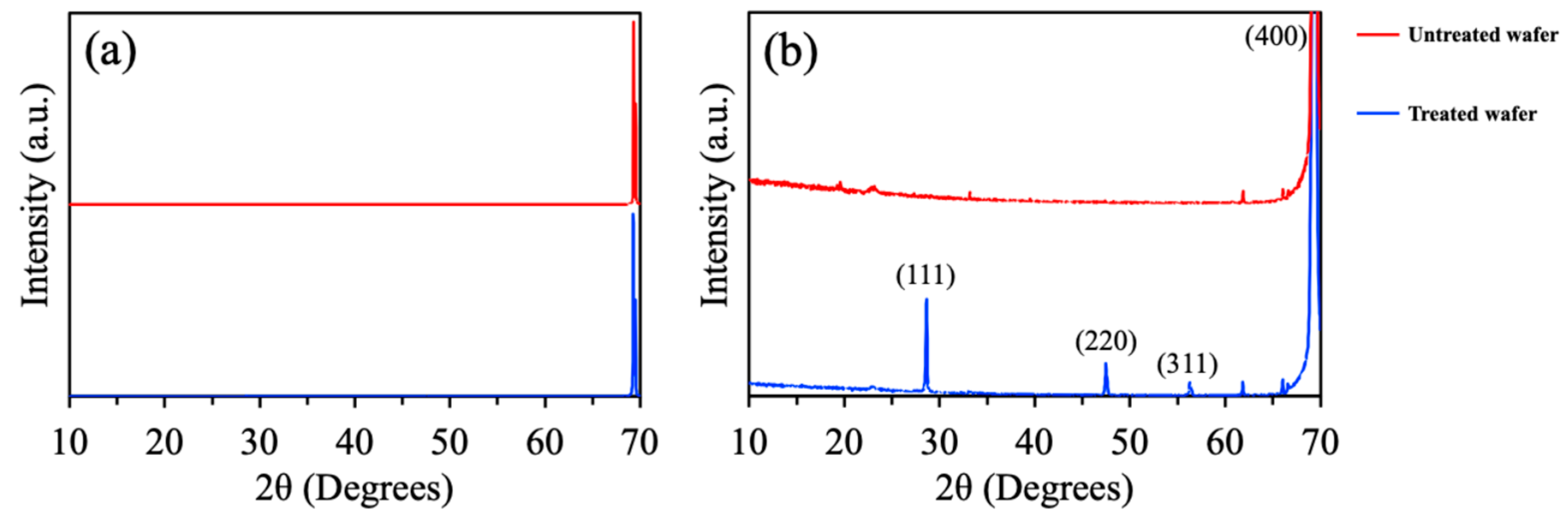
3.1. Material Characterization

The surface morphology of the laser-ablated silicon wafers was examined using SEM (Figure 2). As can be seen in Figure 2a, the laser processing resulted in a well-defined pattern formed by the laser treatment, with uniform spacing between lines ablated into the silicon substrate. At higher magnifications (Figure 2b,c), it was evident that the ablation generated irregularly shaped small particles on the silicon wafer surface. The particles were polydisperse, ranging from tens of micrometers to slightly less than 1 micrometer in length. At the highest magnification (Figure 2c), it was evident that the individual particles also had rough surfaces. These fine particles, combined with their surface roughness, increased the surface area of the Si wafer, which, when subsequently processed into a cell as an electrode, facilitated increasing the achievable rate of electrochemical reactions (all other material properties for the electrode were assumed to be unchanged relative to the untreated Si). It was also noted that some particles were found to cluster within the grooves created during the laser patterning, which may have resulted from localized heating from the laser in the channel regions during the surface treatment. SEM images of an untreated silicon wafer can be found in Supporting Information, Figure S1a,b. As expected, the untreated silicon wafer had a flat surface with no morphological features that would contribute to significant changes in surface area relative to the geometric surface area, even at higher magnifications (Figure S1b).
The treated and untreated Si wafers were also examined using an optical microscope in reflection mode, and example images can be found in the Supporting Information, Figure S2. While finer details of the surface and morphology cannot be observed with the optical micrographs relative to the SEMs, the scale of the line patterns left by the laser were also observed using optical microscopy. Optical microscopy can provide an initial fast assessment of a laser-ablated wafer during sample processing and had overall features consistent with the SEM analysis.
Samples were also prepared for cross-sectional imaging analysis to provide insights into the depth of the morphology changes induced by the laser ablation process. Cross-sectional SEM images of the pristine and laser-treated silicon wafers can be found in the Supporting Information, Figure S1. The pristine wafer (Figure S1c) surface appeared smooth and uniform, without noticeable features or irregularities near the surface region of cross-section. The untreated wafer thus was consistent with an intact and planar structure. In contrast, the cross-section of the laser-treated silicon wafer (Figure S1d) revealed a distinct region from where the laser interacted with the Si substrate. The textured region was approximately 40 µm thick and was clearly visible in the cross-section image. Beneath this layer, the remainder of the wafer remained intact and appeared consistent with the wafer that did not experience any laser ablation with a smooth and planar structure. These results indicated that the laser treatment selectively modified the surface region (within the top < 50 µm) without influencing the rest of the underlying bulk wafer. At higher magnification, the textured surface was observed to have a rugged morphology with a porous and granular structure, indicating the increased surface area seen at the surface of the wafer propagated below the surface throughout the ~40 µm thick region. Cross-sectional optical microscopy images of the pristine, single-treated (ST), and dual-treated (DT) silicon wafers are shown in the Supporting Information, Figure S3. The cross-sectional images (Figure S3b,c) reveal that the ST and DT wafers exhibited similar depths of surface treatments. Consequently, the dual-treated silicon wafer was expected to have morphological properties on both sides comparable to those of the ST wafer.
The structure of laser-ablated silicon wafers was also analyzed using XRD, and the resulting patterns can be found in Figure 3. Both the pristine and laser-treated silicon wafers exhibited a dominant peak at ~69°, corresponding to the (400) crystal plane of silicon [54]. This peak was consistent with the unidirectional crystallinity of the oriented silicon wafers used in this study, confirming that the bulk crystalline structure from regions below those altered by the laser ablation process remained intact with regards to their bulk crystal structure after the laser processing. In addition to the large peak, smaller peaks were also observed for the laser-treated wafer. A magnified y-axis scale is shown in Figure 3b to highlight these peaks. The smaller peaks were also consistent with Si material, with the relevant indices noted on the XRD patterns [55]. These additional peaks were not present for the pristine wafer, and their presence was consistent with the formation of polycrystalline silicon at the wafer surface. Combining the optical and SEM results, we concluded that the laser ablation process resulted in a layer with a higher surface area ~40 µm thick, where the thermal treatment and cooling process generated polycrystalline Si. The Si below the region with increased surface area was still the bulk single crystal Si wafer.

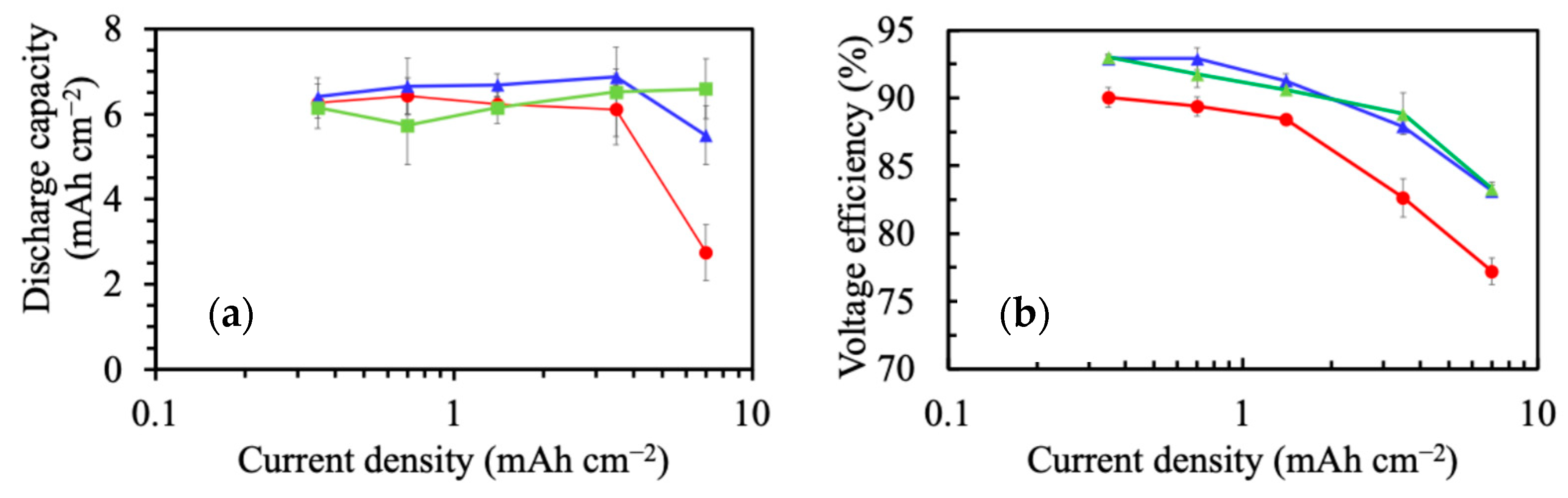
3.2. Electrochemical Characterization

Each of the types of Si wafers (UW, ST, and DT) was used directly as anodes paired with LCO cathodes and assembled into coin cells for electrochemical evaluation. Due to the high overall areal mass of the Si wafer (70 mg cm−2 for UW, 63 mg cm−2 for ST, and 59 mg cm−2 for DT), high reported gravimetric capacity for Si electrode material [17,18], and relatively high irreversible capacity loss reported for Si materials [56,57], it was desirable to pair the Si electrodes with a high areal capacity cathode. Our group has previously reported high areal capacity AAM cathodes using LCO, where the lack of conductive additives or binders provides relative transport advantages in the cell [39,41,42]. AAM LCO cathodes processed using the fabrication method in this work have been previously reported with areal capacities ranging from 21.4 to 45.2 mAh cm−2 [39]. They also have stable reversible charge/discharge cycling, having been reported with extended cycling to retain at least 90.6% capacity relative to first discharge after 50 cycles [39]. Cell coulombic efficiencies with AAM LCO cathodes of ~98% per cycle (after the first cycle) have also been reported when paired with LTO anodes [39,49]. The established cycling retention for the LCO cathodes was important because additional capacity fade would suggest those losses were due to the Si anode.
While the Si anode has an extremely high theoretical areal capacity (~294 mAh cm−2 based on areal mass of Si and reported theoretical capacity of 4200 mAh g−1 [18,19]), it would take an excessively thick cathode, limited to extremely slow rates of charge/discharge, to attempt to obtain a large fraction of this capacity. In addition, prior reports of irreversible capacity loss for Si and fracturing of Si electrodes with lithiation led us to restrict the areal capacity and set this as a limiting property during cell charge/discharge [32,58]. An areal capacity of 7 mAh cm−2 was selected, which was still a relatively high areal capacity compared to other literature reports for similar electrodes [59,60,61]. Also, we estimated the mass within the ~40 µm textured region of the Si electrode was ~2.9 mg cm−2, which suggested that capacity could, in principle, be restricted to only the textured particle region.
Preliminary cells suggested a few charge/discharge cycles were necessary for the delivered discharge capacity to stabilize. Thus, cells were initially cycled for 10 charge/discharge cycles at a relatively low rate (C/25 based on the current density and limits for areal capacity set for the cells). The initial 10 charge/discharge cycles for Si/LCO full cells were thus conducted at a constant current density of 0.28 mA cm−2. The voltage profiles for the first, fifth, and tenth cycles during this initial low-rate cycling can be found in Figure 4. Since during charging cells would achieve the capacity limit (7 mAh cm−2) set by the charging protocol before reaching the voltage cutoff limit, the final charging voltages had some variation between the cells. The charge profiles were relatively consistent throughout these early cycles for a given cell, with relatively small changes in polarization at a given areal capacity and every cycle stopping on reaching the capacity limit. The consistent charge behavior of each cell was also confirmed by their average charge voltages over 10 cycles. The UW, ST, and DT cells exhibited average charge voltages of 3.793 V, 3.791 V, and 3.754 V, respectively, with standard deviations of 0.018 V, 0.026 V, and 0.014 V for the averages calculated from those 10 cycles. The initial coulombic efficiencies were relatively low, measuring 68%, 73%, and 47% for the UW, ST, and DT wafer full cells, respectively. However, by the tenth cycle, the coulombic efficiencies improved to approximately 90%, indicating that the initial low-rate cycling aided in stabilizing the wafer cells. Similar improvements in coulombic efficiency after the initial cycles have also been observed in other studies [30,62].
In the Supporting Information (Figure S4a), LCO half cell charge and discharge profiles can be found, where the charge and discharge profiles had a coulombic efficiency of 94.8% during the first cycle, which improved to over 98% in subsequent cycles (with capacity limited to the same areal capacity as used in the Si/LCO full cells). This high efficiency suggested the AAM LCO electrode should be stable during more extended cycling, even with the relatively high loading and areal capacity. Additionally, no significant voltage rise, typically observed when the majority of available lithium is depleted during cathode charging, was detected [39,63]. This behavior suggested that the LCO electrode retained the available lithium in the electrode beyond the limited capacity of 7 mAh cm−2, ensuring relatively consistent voltage for lithiation/delithiation from the cathode during more extended cycling. In the Supporting Information, Figure S4b–d, the voltage profiles of the Si wafer electrodes used as cathodes paired with lithium metal anodes can be found. All Si wafer configurations exhibited similar voltage curves, indicating consistent lithiation and delithiation processes. The half cell observations combined with prior reports for identically processed AAM LCO gave confidence that any variations in electrochemical outcomes across the full cells could be primarily attributed to differences in the Si wafer electrodes rather than LCO cathode. This analysis was conducted to support the finding that the full cell results effectively isolated the impact of surface treatments and morphological changes in the silicon wafer electrodes, providing a direct comparison of their electrochemical behavior. It is noted here that half cell analysis at the relevant areal capacities with the Si wafer electrodes would not have been reliable due to electrolyte decomposition with the Li anode paired with the chosen electrolyte.
All the Si/LCO full cells exhibited relatively low discharge capacities during the first cycle compared to their charge capacities, thus resulting in initially low coulombic efficiency [64]. As can be found in the Supporting Information, Figure S5, all cells exhibited a gradual increase in discharge capacity over the initial 10 cycles. Figure S5 data points represent the average values from two cells for each wafer electrode type. Cycling at this low rate eventually stabilized the discharge capacity for these Si anode cells. Notably, the laser-treated Si anodes (ST and DT) exhibited a more pronounced capacity increase and higher discharge voltage in the early cycles (Figure S5), attributed to their larger surface area, which increased electroactive surface area and reduced interfacial resistance for electrochemical reactions. This speculation was supported by EIS from Si/LCO cells freshly made and after the initial slow cycles (Figure S6a,b), where charge transfer resistance was the largest for the UW cell. These electrochemical outcomes indicated that the increased surface area from laser treatment effectively lowered the interfacial resistance. Additionally, the enhancement likely improved electrolyte access, accelerating stabilization of the solid electrolyte interphase (SEI) relative to the UW wafer. It is noted here that more surface area for SEI is not necessarily always beneficial, as accelerated SEI growth can increase cell resistance and consume electrolytes. Within the conditions of these initial experiments, these factors were not likely to be issues, but in conditions such as more electrolyte lean cells, additional SEI may be a challenge.
For cells with the three different types of Si anodes, the charge capacities were all the same because this capacity was controlled by the charging protocol. The tenth cycle discharge capacities were also approximately the same for the three different cells. However, the voltage efficiencies (relative average voltage of discharge compared to charge process) were different for the cells depending on the anode used. All cells gradually increased in voltage efficiency for the first 10 cycles; however, by the final cycle, the DT and ST anode cells had voltage efficiencies of ~93%. However, the UW anode cell had a tenth cycle voltage efficiency of 90%. Because the only difference between the cells was whether or not the Si electrode had undergone laser ablation processing, it was speculated that the voltage efficiency resulted from differences in Si surface area in contact with the electrolyte phase due to the higher surface area after the laser ablation processing. The increased surface area would be expected to reduce the interfacial overpotential for both the charge and discharge processes, thus improving round trip voltage efficiency.
After the initial 10 charge/discharge cycles at a low rate had concluded, rate capability testing was conducted on each cell to evaluate the retention of capacity at increasing rates/current densities. For rate capability evaluation, the cells continued to be charged at the low rate of 0.28 mA cm−2, with the same voltage and capacity cutoff as the low-rate cycling. However, for the rate capability evaluation, the discharge current was increased every five cycles. The highest discharge current evaluated was 7.0 mA cm−2, which, based on the charge capacity limit, would correspond to ~1C. The average discharge capacity and voltage efficiency for the different rates of discharge can be found in Figure 5 and each data point reflects the averaged values from two cells per electrode type to improve data reliability and ensure reproducibility. Error bars represent the standard deviation of the five cycles at that rate used to calculate each average value. All cells exhibited similar discharge capacities up to a current density of 3.5 mA cm−2, indicating consistent electrochemical cycling capabilities for relatively low current density discharge cycling. However, differences were observed depending on the Si anode processing at higher current densities, with the difference most pronounced at the highest current density of 7.0 mA cm−2. At this highest current density, the ST and DT laser-ablated silicon wafer anode cells demonstrated higher discharge capacities, and thus, higher rate capability, compared to the UW Si electrode cells [30]. The voltage efficiency outcomes further supported the influence of the surface laser ablation of the silicon wafers on electrochemical outcomes. As can be found in the Supporting Information, Figure S7b, the Si electrodes that had laser ablation treatment consistently achieved higher voltage efficiencies than the UW electrode cells across all current densities and cycles, suggesting reduced polarization and improved energy utilization.
The improved rate capability for the DT Si cell relative to the ST Si cell was not expected as both had only a single laser-ablated interface in contact with the electrolyte directly across from the LCO electrode, and thus, only one ablated interface was expected to participate in electrochemical reactions. However, we speculate the differences may have been due to improved contact between the silicon wafer surface and the current collector for the DT Si electrode cell. Laser ablating and increasing surface area on the second side of the Si electrode provided a rough interface for the bottom (current collector) side of the Si wafer. Although, in principle, a flat current collector and flat Si wafer interface would provide an efficient pathway for electron transfer between the current collector (a stainless steel thin plate) and the Si electrode, slight deviations from being flat would result in large regions of the current collector/electrode interface not in contact. Thus, we speculate that the roughness from the laser ablation of the bottom side of the Si helped to maintain contact with the current collector, which reduced electronic conductivity resistance and more uniformly spread the current distribution and utilization of the Si electrode.
Although this study focused on a single laser-ablated pattern, future research will investigate the impact of different laser patterns on electrode performance. This present study demonstrated the effects of laser ablation as a surface treatment for Si wafer electrodes. The laser-ablated Si electrode demonstrated high capacity retention even at an increased current density of 7 mA cm−2 in a full cell. Although the electrode fabrication methods and experimental conditions differ from other previously reported studies, it is notable that many efforts to create high areal capacity Si anodes have primarily been applied in half cell, with capacities often failing to exceed 4 mAh cm−2 [59,61,65,66,67]. While some studies have reported higher areal capacities than our benchmark of 7 mAh cm−2, these results were achieved under lower current densities compared to the conditions used in this work [30,31]. Thus, laser ablating Si produces electrodes that can be reversibly cycled with relatively high combinations of areal capacity and areal current densities.

4. Conclusions

In this study, the effects of laser ablation as a surface modification for silicon wafers was investigated for when the wafers were used as electrodes in lithium-ion batteries. Laser-treated silicon wafers, both with single and double-sided ablation treatment, exhibited improved electrochemical properties compared to untreated Si wafer anodes. The laser-treated electrodes demonstrated higher capacity retention and improved rate capability, particularly at the highest discharge current densities evaluated. These improvements were attributed to the increased surface area from the polycrystalline silicon layer formed during the laser ablation process. The dual-sided treatment further contributed to improved electrochemical outcomes, which were speculated to result from improved contact between the silicon wafer electrode and the current collector. Pairing the silicon wafer electrodes with AAM LCO cathodes enabled the realization of high areal capacity full cells at 7 mAh cm−2. This work highlighted the potential of laser ablation for improving the electrochemical properties of silicon wafers used as battery anodes. While producing silicon wafers would be relatively expensive for a rechargeable battery application, future efforts will investigate the feasibility of sourcing such wafers from alternative sources such as end-of-life photovoltaic panels.

Supplementary Materials

The following supporting information can be downloaded at https://www.mdpi.com/article/10.3390/batteries11040121/s1: Figure S1:Scanning electron microscopy (SEM) images for untreated Si wafer and cross-section images for untreated and laser-treated Si wafers; Figure S2: Si wafer optical microscope images collected in reflection mode; Figure S3: Optical microscope cross-section images; Figure S4: Voltage profiles for AAM-LCO and Si wafer electrode half cells; Figure S5: Discharge capacity during low-rate charge and discharge cycling of Si/LCO full cells for the initial 10 cycles, voltage efficiency, and charge and discharge voltage corresponding to those same cycles; Figure S6: Nyquist plot from EIS of freshly made Si/LCO cells, and after initial 10 cycles; Figure S7: Discharge capacity during low-rate charge and increasing rates of discharge cycling of Si/LCO full cells, voltage efficiency, charge and discharge voltage corresponding to those same cycles.

Author Contributions

Conceptualization, G.M.K.J. and M.C.G.; methodology, G.M.K.J. and M.C.G.; formal analysis, B.M., C.C. and G.M.K.J.; investigation, B.M., A.C., C.C., G.M.K.J. and M.C.G.; resources, G.M.K.J. and M.C.G.; data curation, B.M.; writing—original draft preparation, B.M. and A.C.; writing—review and editing, B.M., G.M.K.J. and M.C.G.; visualization, B.M., G.M.K.J. and M.C.G.; supervision, G.M.K.J. and M.C.G.; project administration, G.M.K.J. and M.C.G.; funding acquisition, G.M.K.J. and M.C.G. All authors have read and agreed to the published version of the manuscript.

Funding

This work was supported by a CoLab grant from UVA’s Environmental Institute.

Data Availability Statement

The data presented in this study are available on request from the corresponding author. The data are not publicly available due to privacy.

Conflicts of Interest

The authors declare no conflicts of interest. The funders had no role in the design of this study; in the collection, analyses, or interpretation of data; in the writing of the manuscript; or in the decision to publish the results.

Abbreviations

The following abbreviations are used in this manuscript:
PVPhotovoltaic
LiLithium
LCOLiCoO2
SiSilicon
AAMAll-active material
UWUntreated wafer
STSingle-treated wafer
DTDual-treated wafer

References

  1. Ghoniem, R.M.; Alahmer, A.; Rezk, H.; As’ad, S. Optimal Design and Sizing of Hybrid Photovoltaic/Fuel Cell Electrical Power System. Sustainability 2023, 15, 12026. [Google Scholar] [CrossRef]
  2. Esmaeili, M.; Ahmadi, A.A.; Nateghi, A.; Shafie-khah, M. Robust Power Management System with Generation and Demand Prediction and Critical Loads in DC Microgrid. J. Clean. Prod. 2023, 384, 135490. [Google Scholar] [CrossRef]
  3. Olabi, A.G.; Abdelkareem, M.A. Renewable Energy and Climate Change. Renew. Sustain. Energy Rev. 2022, 158, 112111. [Google Scholar] [CrossRef]
  4. Ang, T.Z.; Salem, M.; Kamarol, M.; Das, H.S.; Nazari, M.A.; Prabaharan, N. A Comprehensive Study of Renewable Energy Sources: Classifications, Challenges and Suggestions. Energy Strat. Rev. 2022, 43, 100939. [Google Scholar] [CrossRef]
  5. Mariotti, N.; Bonomo, M.; Fagiolari, L.; Barbero, N.; Gerbaldi, C.; Bella, F.; Barolo, C. Recent Advances in Eco-Friendly and Cost-Effective Materials towards Sustainable Dye-Sensitized Solar Cells. Green Chem. 2020, 22, 7168–7218. [Google Scholar] [CrossRef]
  6. Lee, S.; Jeong, D.; Kim, C.; Lee, C.; Kang, H.; Woo, H.Y.; Kim, B.J. Eco-Friendly Polymer Solar Cells: Advances in Green-Solvent Processing and Material Design. ACS Nano 2020, 14, 14493–14527. [Google Scholar] [CrossRef]
  7. Chowdhury, M.S.; Rahman, K.S.; Chowdhury, T.; Nuthammachot, N.; Techato, K.; Akhtaruzzaman, M.; Tiong, S.K.; Sopian, K.; Amin, N. An Overview of Solar Photovoltaic Panels’ End-of-Life Material Recycling. Energy Strat. Rev. 2020, 27, 100431. [Google Scholar] [CrossRef]
  8. Peplow, M. Solar Panels Face Recycling Challenge. ACS Cent. Sci. 2022, 8, 299–302. [Google Scholar] [CrossRef]
  9. Farrell, C.C.; Osman, A.I.; Doherty, R.; Saad, M.; Zhang, X.; Murphy, A.; Harrison, J.; Vennard, A.S.M.; Kumaravel, V.; Al-Muhtaseb, A.H.; et al. Technical Challenges and Opportunities in Realising a Circular Economy for Waste Photovoltaic Modules. Renew. Sustain. Energy Rev. 2020, 128, 109911. [Google Scholar] [CrossRef]
  10. Preet, S.; Smith, S.T. A Comprehensive Review on the Recycling Technology of Silicon Based Photovoltaic Solar Panels: Challenges and Future Outlook. J. Clean. Prod. 2024, 448, 141661. [Google Scholar] [CrossRef]
  11. Shin, J.; Park, J.; Park, N. A Method to Recycle Silicon Wafer from End-of-Life Photovoltaic Module and Solar Panels by Using Recycled Silicon Wafers. Sol. Energy Mater. Sol. Cells 2017, 162, 1–6. [Google Scholar] [CrossRef]
  12. Liu, T.; Dong, T.; Wang, M.; Du, X.; Sun, Y.; Xu, G.; Zhang, H.; Dong, S.; Cui, G. Recycled Micro-Sized Silicon Anode for High-Voltage Lithium-Ion Batteries. Nat. Sustain. 2024, 7, 1057–1066. [Google Scholar] [CrossRef]
  13. Sreenarayanan, B.; Vicencio, M.; Bai, S.; Lu, B.; Mao, O.; Adireddy, S.; Bao, W.; Meng, Y.S. Recycling Silicon Scrap for Spherical Si–C Composite as High-Performance Lithium-Ion Battery Anodes. J. Power Sources 2023, 578, 233245. [Google Scholar] [CrossRef]
  14. Pham, T.K.; Shin, J.H.; Karima, N.C.; Jun, Y.S.; Jeong, S.K.; Cho, N.; Lee, Y.W.; Cho, Y.; Lim, S.N.; Ahn, W. Application of Recycled Si from Industrial Waste towards Si/RGO Composite Material for Long Lifetime Lithium-Ion Battery. J. Power Sources 2021, 506, 230244. [Google Scholar] [CrossRef]
  15. Bao, Q.; Huang, Y.H.; Lan, C.K.; Chen, B.H.; Duh, J.G. Scalable Upcycling Silicon from Waste Slicing Sludge for High-Performance Lithium-Ion Battery Anodes. Electrochim. Acta 2015, 173, 82–90. [Google Scholar] [CrossRef]
  16. Rahman, M.M.; Mateti, S.; Sultana, I.; Hou, C.; Falin, A.; Cizek, P.; Glushenkov, A.M.; Chen, Y. End-of-Life Photovoltaic Recycled Silicon: A Sustainable Circular Materials Source for Electronic Industries. Adv. Energy Sustain. Res. 2021, 2, 202100081. [Google Scholar] [CrossRef]
  17. Shi, J.; Zu, L.; Gao, H.; Hu, G.; Zhang, Q. Silicon-Based Self-Assemblies for High Volumetric Capacity Li-Ion Batteries via Effective Stress Management. Adv. Funct. Mater. 2020, 30, 202002980. [Google Scholar] [CrossRef]
  18. Szczech, J.R.; Jin, S. Nanostructured Silicon for High Capacity Lithium Battery Anodes. Energy Env. Sci. 2011, 4, 56–72. [Google Scholar] [CrossRef]
  19. Chen, X.; Li, H.; Yan, Z.; Cheng, F.; Chen, J. Structure Design and Mechanism Analysis of Silicon Anode for Lithium-Ion Batteries. Sci. China Mater. 2019, 62, 1515–1536. [Google Scholar] [CrossRef]
  20. Zuo, X.; Zhu, J.; Müller-Buschbaum, P.; Cheng, Y.J. Silicon Based Lithium-Ion Battery Anodes: A Chronicle Perspective Review. Nano Energy 2017, 31, 113–143. [Google Scholar] [CrossRef]
  21. Dou, F.; Weng, Y.; Wang, Q.; Chen, G.; Liu, H.; Shi, L.; Zhang, D. In Situ Imaging Analysis of the Inhibition Effect of Functional Coating on the Volume Expansion of Silicon Anodes. Chem. Eng. J. 2021, 417, 128122. [Google Scholar] [CrossRef]
  22. Ashuri, M.; He, Q.; Shaw, L.L. Silicon as a Potential Anode Material for Li-Ion Batteries: Where Size, Geometry and Structure Matter. Nanoscale 2016, 8, 74–103. [Google Scholar] [CrossRef] [PubMed]
  23. Dai, F.; Yi, R.; Yang, H.; Zhao, Y.; Luo, L.; Gordin, M.L.; Sohn, H.; Chen, S.; Wang, C.; Zhang, S.; et al. Minimized Volume Expansion in Hierarchical Porous Silicon upon Lithiation. ACS Appl. Mater. Interfaces 2019, 11, 13257–13263. [Google Scholar] [CrossRef]
  24. Wu, F.; Dong, Y.; Su, Y.; Wei, C.; Chen, T.; Yan, W.; Ma, S.; Ma, L.; Wang, B.; Chen, L.; et al. Benchmarking the Effect of Particle Size on Silicon Anode Materials for Lithium-Ion Batteries. Small 2023, 19, e202301301. [Google Scholar] [CrossRef]
  25. Chan, C.K.; Peng, H.; Liu, G.; McIlwrath, K.; Zhang, X.F.; Huggins, R.A.; Cui, Y. High-Performance Lithium Battery Anodes Using Silicon Nanowires. Nat. Nanotechnol. 2008, 3, 31–35. [Google Scholar] [CrossRef]
  26. Wang, H.C.; Muruganantham, R.; Hsieh, C.T.; Liu, W.R. Electrochemical Elucidation of Phosphorus-Doped and 3D Graphene Aerogel Surface-Modified SiOx Porous Nanocomposite Electrode Material for High-Performance Lithium-Ion Batteries. Electrochim. Acta 2024, 477, 143775. [Google Scholar] [CrossRef]
  27. Muruganantham, R.; Yang, C.W.; Wang, H.J.; Huang, C.H.; Liu, W.R. Industrial Silicon-Wafer-Wastage-Derived Carbon-Enfolded Si/Si-C/C Nanocomposite Anode Material through Plasma-Assisted Discharge Process for Rechargeable Li-Ion Storage. Nanomaterials 2022, 12, 659. [Google Scholar] [CrossRef]
  28. Wei, D.; Mao, J.; Zheng, Z.; Fang, J.; Luo, Y.; Gao, X. Achieving a High Loading Si Anode via Employing a Triblock Copolymer Elastomer Binder, Metal Nanowires and a Laminated Conductive Structure. J. Mater. Chem. A Mater. 2018, 6, 20982–20991. [Google Scholar] [CrossRef]
  29. Zhao, X.; Lehto, V.P. Challenges and Prospects of Nanosized Silicon Anodes in Lithium-Ion Batteries. Nanotechnology 2021, 32, 042002. [Google Scholar] [CrossRef]
  30. Na, I.; Kim, H.; Kunze, S.; Nam, C.; Jo, S.; Choi, H.; Oh, S.; Choi, E.; Song, Y.B.; Jung, Y.S.; et al. Monolithic 100% Silicon Wafer Anode for All-Solid-State Batteries Achieving High Areal Capacity at Room Temperature. ACS Energy Lett. 2023, 8, 1936–1943. [Google Scholar] [CrossRef]
  31. Yang, C.; Chandran, K.S.R. Photolithographic Structuring of Ordered Silicon Micropillar Electrodes for Lithium-Ion Batteries and Electrochemical Performance. ACS Appl. Energy Mater. 2023, 6, 5930–5939. [Google Scholar] [CrossRef]
  32. Shi, F.; Song, Z.; Ross, P.N.; Somorjai, G.A.; Ritchie, R.O.; Komvopoulos, K. Failure Mechanisms of Single-Crystal Silicon Electrodes in Lithium-Ion Batteries. Nat. Commun. 2016, 7, 11886. [Google Scholar] [CrossRef] [PubMed]
  33. Yan, J.; Noguchi, J.; Terashi, Y. Fabrication of Single-Crystal Silicon Micro Pillars on Copper Foils by Nanosecond Pulsed Laser Irradiation. CIRP Ann. Manuf. Technol. 2017, 66, 253–256. [Google Scholar] [CrossRef]
  34. Thakur, M.; Isaacson, M.; Sinsabaugh, S.L.; Wong, M.S.; Biswal, S.L. Gold-Coated Porous Silicon Films as Anodes for Lithium Ion Batteries. J. Power Sources 2012, 205, 426–432. [Google Scholar] [CrossRef]
  35. Park, J.; Suh, S.; Jeong, S.; Kim, H.J. New Approach for the High Electrochemical Performance of Silicon Anode in Lithium-Ion Battery: A Rapid and Large Surface Treatment Using a High-Energy Pulsed Laser. J. Power Sources 2021, 491, 229573. [Google Scholar] [CrossRef]
  36. Je, M.; Han, D.Y.; Ryu, J.; Park, S. Constructing Pure Si Anodes for Advanced Lithium Batteries. Acc. Chem Res. 2023, 56, 2213–2224. [Google Scholar] [CrossRef] [PubMed]
  37. Li, P.; Hwang, J.Y.; Sun, Y.K. Nano/Microstructured Silicon-Graphite Composite Anode for High-Energy-Density Li-Ion Battery. ACS Nano 2019, 13, 2624–2633. [Google Scholar] [CrossRef]
  38. Cai, C.; Hensley, D.; Koenig, G.M. High Capacity Rechargeable Coin Cells Using All Active Material Electrodes and Percolated Networks of LiCoO2 Blended with LiNi0.8Co0.15Al0.05O2. J. Alloys Compd. 2023, 968, 171965. [Google Scholar] [CrossRef]
  39. Robinson, J.P.; Ruppert, J.J.; Dong, H.; Koenig, G.M. Sintered Electrode Full Cells for High Energy Density Lithium-Ion Batteries. J. Appl. Electrochem. 2018, 48, 1297–1304. [Google Scholar] [CrossRef]
  40. Cai, C.; Min, B.; Yost, D.; Koenig, G.M. Combining Ester Solvent-Containing Electrolytes with All-Active Material Electrodes for High Current Density Lithium-Ion Batteries. ACS Appl. Energy Mater. 2023, 6, 11226–11233. [Google Scholar] [CrossRef]
  41. Cai, C.; Koenig, G.M. Processing Temperature Impact on TiNb 2 O 7 Thick All Active Material Lithium-Ion Battery Electrodes. J. Electrochem. Soc. 2023, 170, 010529. [Google Scholar] [CrossRef]
  42. Thorat, I.V.; Stephenson, D.E.; Zacharias, N.A.; Zaghib, K.; Harb, J.N.; Wheeler, D.R. Quantifying Tortuosity in Porous Li-Ion Battery Materials. J. Power Sources 2009, 188, 592–600. [Google Scholar] [CrossRef]
  43. Khetri, M.; Gupta, M.C. Recycling of Silver from Silicon Solar Cells by Laser Debonding. Sol. Energy 2024, 270, 112381. [Google Scholar] [CrossRef]
  44. Gottumukkala, N.R.; Gupta, M.C. Laser Processing of Sapphire and Fabrication of Diffractive Optical Elements. Appl Opt. 2022, 61, 2391. [Google Scholar] [CrossRef] [PubMed]
  45. Chakraborty, A.; Gottumukkala, N.R.; Gupta, M.C. Superhydrophobic Surface by Laser Ablation of PDMS. Langmuir 2023, 39, 11259–11267. [Google Scholar] [CrossRef]
  46. Cai, C.; Koenig, G.M. Enhancing Low Electronic Conductivity Materials in All Active Material Electrodes through Multicomponent Architecture. Energy Adv. 2023, 2, 308–320. [Google Scholar] [CrossRef]
  47. Nie, Z.; Ong, S.; Hussey, D.S.; Lamanna, J.M.; Jacobson, D.L.; Koenig, G.M. Probing Transport Limitations in Thick Sintered Battery Electrodes with Neutron Imaging. Mol. Syst. Des. Eng. 2020, 5, 245–256. [Google Scholar] [CrossRef]
  48. Cai, C.; Hensley, D.; Koenig, G.M. Simulated Discharge Overpotential Distributions for Sintered Electrode Batteries in Rechargeable Coin Cell Form Factors. J. Energy Storage 2022, 54, 105218. [Google Scholar] [CrossRef]
  49. Nie, Z.; Parai, R.; Cai, C.; Michaelis, C.; LaManna, J.M.; Hussey, D.S.; Jacobson, D.L.; Ghosh, D.; Koenig, G.M. Pore Microstructure Impacts on Lithium Ion Transport and Rate Capability of Thick Sintered Electrodes. J. Electrochem. Soc. 2021, 168, 060550. [Google Scholar] [CrossRef]
  50. Yoon, T.; Nguyen, C.C.; Seo, D.M.; Lucht, B.L. Capacity Fading Mechanisms of Silicon Nanoparticle Negative Electrodes for Lithium Ion Batteries. J. Electrochem. Soc. 2015, 162, A2325–A2330. [Google Scholar] [CrossRef]
  51. Chae, S.; Ko, M.; Kim, K.; Ahn, K.; Cho, J. Confronting Issues of the Practical Implementation of Si Anode in High-Energy Lithium-Ion Batteries. Joule 2017, 1, 47–60. [Google Scholar] [CrossRef]
  52. Zheng, H.; Li, J.; Song, X.; Liu, G.; Battaglia, V.S. A Comprehensive Understanding of Electrode Thickness Effects on the Electrochemical Performances of Li-Ion Battery Cathodes. Electrochim. Acta 2012, 71, 258–265. [Google Scholar] [CrossRef]
  53. Singh, M.; Kaiser, J.; Hahn, H. Thick Electrodes for High Energy Lithium Ion Batteries. J. Electrochem. Soc. 2015, 162, A1196–A1201. [Google Scholar] [CrossRef]
  54. Hwang, B.-H. Calculation and Measurement of All (002) Multiple Diffraction Peaks from a (001) Silicon Wafer. J. Phys. D Appl. Phys. 2001, 34, 2469–2474. [Google Scholar] [CrossRef]
  55. Wahab, R.; Ahmad, N.; Alam, M. Silicon Nanoparticles: A New and Enhanced Operational Material for Nitrophenol Sensing. J. Mater. Sci. Mater. Electron. 2020, 31, 17084–17099. [Google Scholar] [CrossRef]
  56. Delpuech, N.; Dupre, N.; Moreau, P.; Bridel, J.S.; Gaubicher, J.; Lestriez, B.; Guyomard, D. Mechanism of Silicon Electrode Aging upon Cycling in Full Lithium-Ion Batteries. ChemSusChem 2016, 9, 841–848. [Google Scholar] [CrossRef]
  57. Ezzedine, M.; Jardali, F.; Florea, I.; Zamfir, M.R.; Cojocaru, C.S. Nanostructuring Strategies for Silicon-Based Anodes in Lithium-Ion Batteries: Tuning Areal Silicon Loading, SEI Formation/Irreversible Capacity Loss, Rate Capability Retention and Electrode Durability. Batter. Supercaps 2023, 6, 202200451. [Google Scholar] [CrossRef]
  58. Chew, H.B.; Hou, B.; Wang, X.; Xia, S. Cracking Mechanisms in Lithiated Silicon Thin Film Electrodes. Int. J. Solids Struct. 2014, 51, 4176–4187. [Google Scholar] [CrossRef]
  59. Peng, K.; Jie, J.; Zhang, W.; Lee, S.T. Silicon Nanowires for Rechargeable Lithium-Ion Battery Anodes. Appl. Phys. Lett. 2008, 93, 033105. [Google Scholar] [CrossRef]
  60. Farid, G.; Amade-Rovira, R.; Ospina, R.; Bertran-Serra, E. Surface Modification of Silicon Nanowires via Drop-Casting for High-Performance Li-Ion Battery Electrodes: SiNWs Decorated with Molybdenum Oxide Nanoparticles. J. Energy Storage 2024, 78, 110104. [Google Scholar] [CrossRef]
  61. Lau, D.; Hall, C.A.; Lim, S.; Yuwono, J.A.; Burr, P.A.; Song, N.; Lennon, A. Reduced Silicon Fragmentation in Lithium Ion Battery Anodes Using Electronic Doping Strategies. ACS Appl. Energy Mater. 2020, 3, 1730–1741. [Google Scholar] [CrossRef]
  62. Nugroho, A.P.; Hawari, N.H.; Prakoso, B.; Refino, A.D.; Yulianto, N.; Iskandar, F.; Kartini, E.; Peiner, E.; Wasisto, H.S.; Sumboja, A. Vertically Aligned N-Type Silicon Nanowire Array as a Free-Standing Anode for Lithium-Ion Batteries. Nanomaterials 2021, 11, 3137. [Google Scholar] [CrossRef] [PubMed]
  63. Qi, Z.; Koenig, G.M. High-Performance LiCoO2 Sub-Micrometer Materials from Scalable Microparticle Template Processing. ChemistrySelect 2016, 1, 3992–3999. [Google Scholar] [CrossRef]
  64. Lee, P.-K.; Li, Y.; Yu, D.Y.W. Insights from Studying the Origins of Reversible and Irreversible Capacities on Silicon Electrodes. J. Electrochem. Soc. 2017, 164, A6206–A6212. [Google Scholar] [CrossRef]
  65. Marinaro, M.; Weinberger, M.; Wohlfahrt-Mehrens, M. Toward Pre-Lithiatied High Areal Capacity Silicon Anodes for Lithium-Ion Batteries. Electrochim. Acta 2016, 206, 99–107. [Google Scholar] [CrossRef]
  66. Chen, Z.; Wang, C.; Lopez, J.; Lu, Z.; Cui, Y.; Bao, Z. High-Areal-Capacity Silicon Electrodes with Low-Cost Silicon Particles Based on Spatial Control of Self-Healing Binder. Adv. Energy Mater. 2015, 5, 201401826. [Google Scholar] [CrossRef]
  67. Lee, G.; Schweizer, S.L.; Wehrspohn, R.B. Electrochemical Characteristics of Plasma-Etched Black Silicon as Anodes for Li-Ion Batteries. J. Vac. Sci. Technol. A Vac. Surf. Film. 2014, 32, 4897609. [Google Scholar] [CrossRef]
Figure 1. Cartoon schematic for (a) the initial untreated wafer (UW) of Si, (b) the Si wafer which had laser ablation treatment on a single side, referred to as a single-treated (ST) wafer, and (c) a Si wafer with laser ablation treatment on both sides, referred to as a dual-treated (DT) wafer. (d) Materials assembled into coin cells used for electrochemical evaluation.
Batteries 11 00121 g001
Figure 2. Scanning electron microscopy images for a laser-ablated Si electrode at relatively (a) low magnification, (b) higher magnification, and (c) highest magnification.
Batteries 11 00121 g002
Figure 3. (a) XRD patterns for the silicon wafers with (blue) and without (red) laser ablation treatment. (b) The same pattern as in (a), except that the y-axis has been restricted such that the smaller peaks resulting from polycrystalline Si at the surface can be more clearly observed. Indexing based on the reference pattern for Si [55].
Batteries 11 00121 g003
Figure 4. Voltage profiles for the first, fifth, and tenth cycles of (a) UW, (b) ST, and (c) DT Si wafer anodes paired with LCO cathodes during full cell low-rate cycling. Cycles displayed are for the first cycle (green), fifth cycle (orange), and tenth cycle (purple). The charge and discharge current density for all cycles was 0.28 mA cm−2.
Batteries 11 00121 g004
Figure 5. Average (a) discharge capacity and (b) voltage efficiency for Si/LCO full cells. Cells had five cycles at each current density, and the error bars are the standard deviations of the average of the five cycles at each current for a given cell. Each data point represents the averaged results from two cells per electrode type to improve data confidence and reproducibility. The three Si anodes were UW (red circles), ST (blue triangles), and DT (green squares).
Batteries 11 00121 g005
Disclaimer/Publisher’s Note: The statements, opinions and data contained in all publications are solely those of the individual author(s) and contributor(s) and not of MDPI and/or the editor(s). MDPI and/or the editor(s) disclaim responsibility for any injury to people or property resulting from any ideas, methods, instructions or products referred to in the content.

