Review

Two-Dimensional Doped Materials

1
Research Institute of Hunan University in Chongqing, Chongqing 401120, China
2
Institute of Photoelectronic Thin Film Devices and Technology of Nankai University, Tianjin 300350, China
3
Advanced Semiconductor Technology and Application Engineering Research Center of Ministry of Education of China, College of Semiconductors (College of Integrated Circuits), Hunan University, Changsha 410082, China
4
Shenzhen Research Institute of Hunan University, Shenzhen 518063, China
5
College of Chemistry and Chemical Engineering, Hunan University, Changsha 410082, China
*
Authors to whom correspondence should be addressed.
Magnetochemistry 2022, 8(12), 172; https://doi.org/10.3390/magnetochemistry8120172
Submission received: 14 October 2022 / Revised: 4 November 2022 / Accepted: 17 November 2022 / Published: 29 November 2022
(This article belongs to the Special Issue Advances in Magnetic Two Dimensional Materials)

Abstract

:
The recently intensified research in atomically thick two-dimensional (2D) materials has been motivated by their unique properties and the possibility of updating the future electronic and optoelectronic technologies. Doping can change the band structure of a semiconductor and regulate its physical and chemical properties. Doping has a significant effect on the electronic structure of 2D materials due to their atomic thickness. Here, we present a tutorial review of 2D doped materials (except graphene), including various doping types and theoretical calculations, the preparation and characterization methods, and its multifunctional application. Finally, we will summarize by stating the current challenges and future opportunities in the development of 2D doped materials.

1. Introduction

In 2004, A. K. Geim and K. S. Novoselov discovered graphene from bulk graphite, opening the door to the study of two-dimensional materials (2DMs) [1]. Two-dimensional materials possess an atomic thickness and their intralayer atoms are combined by covalent bonds in nature, whereas the interlayers are coupled by weak van der Waals forces, thus allowing the crystal to readily cleave along the layer’s surface [2,3,4,5]. A variety of 2DMs have been found experimentally, including hexagonal boron nitride (hBN), transition metal dichalcogenides (TMDs), and layered metal oxides [6,7,8,9,10,11]. It is reported that there should be more than 1000 kinds of 2DMs in the world by high-throughput calculations [12]. The diverse families of 2DMs display versatile properties with potential applications in field effect transistors, optoelectronic devices, energy storage, and conversion, catalysis, and biomedicine [13,14,15]. In order to maximize the application of 2DMs, it is necessary to develop several approaches to modulate their properties, including constructing a heterostructure, fabricating a novel device, and doping [16,17,18,19].
In classical semiconductor theory, doping is the intentional introduction of impurities into a material, which is fundamental to controlling the properties of bulk semiconductors [20]. A doping semiconductor can change its band structure, including the size of the band gap, the type of the carrier, and the location of the Fermi level, and thus regulate its electrical, optical, electrochemical, and magnetic properties [21,22,23]. The development of modern semiconductor technology is based on the theoretical research and technological innovation of semiconductor doping. Compared with bulk materials, 2DMs are very sensitive to the external factors for the unique structure where almost all the atoms are exposed to the surface. Thus, the band structures of 2DMs can be more validly tuned by various doping approaches [24,25,26,27,28].
Herein, we present a forward-looking review article that discusses the state-of-the-art in 2D doped materials. Initially, we will outline the different types and theoretical calculations of 2D doped materials. Additionally, we will discuss the various strategies to doping 2DMs and how to characterize them. Finally, we will highlight the optical, electronic, magnetic, and electrochemical properties of 2D doped materials and address future directions which have yet to be explored for novel 2D doped materials intended for various practical applications.

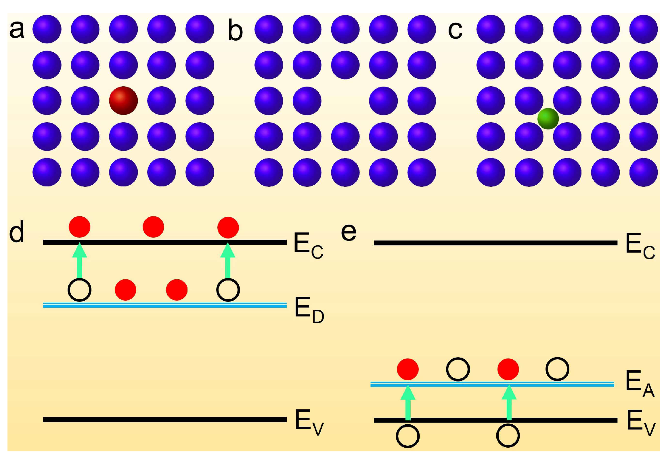
2. Classic Semiconductor Doping Type

Doping can tune the electrical property of a semiconductor, which greatly promotes the progress of semiconductor integration technology [29]. There are two main doping technologies for a semiconductor: thermal diffusion and ion implantation. The former is to heat the semiconductor, which intensifies the thermal motion of the atom, so that the intrinsic atom can obtain enough energy to leave a vacancy away from the lattice or make the impurity atoms diffuse in the intrinsic semiconductor. The latter is to ionize impurity atoms into ions and accelerate them with a strong electric field to obtain high kinetic energy, then directly bombard the intrinsic semiconductor to achieve an impurity injection. Here, we will give a brief analysis of the three doping types, including substitutional doping, vacancy, and interstitial doping [30].

2.1. Substitutional Doping

Substitutional doping, which is where one atom replaces another one to form a new semiconductor, is a common type of doping in semiconductor integrated process (Figure 1a). Substitutional doping often occurs in the location where there are vacancies in the material, rather than exchanging positions with the host material. At the same time, the size of the impurity atom and host atom is similar.

2.2. Vacancy

Many semiconductor materials are grown at relatively high temperatures, and there will be more vacancies in the body at high temperatures (Figure 1b). At a certain temperature, there is a certain equilibrium value. When the crystal cools down at a fast rate, some vacancies are frozen to form nonequilibrium vacancies, which affects the physical properties of the semiconductor.

2.3. Interstitial Doping

In the process of a thermal diffusion and ion implantation, a part of the atoms get enough energy to overcome the binding of the surrounding atoms and squeeze into the gap between the atoms to form interstitial atoms (Figure 1c), which will have a great impact on the electrical, optical, and electrochemical properties of semiconductors.
The doping mechanism of n-type and p-type semiconductors are shown in Figure 1d,e, respectively. When the majority carriers of a semiconductor are electrons, they are called n-type semiconductors. When the majority carriers are holes, they are called p-type semiconductors. An n-type semiconductor can be obtained by doping phosphorus in monocrystalline silicon, while a p-type semiconductor can be formed by a doping boron. N-type and p-type semiconductors are the cornerstones of integrated circuits.
After doping in intrinsic semiconductors, the donor and acceptor impurity levels will be introduced. Since ED is very close to EC, the electron at the donor level can transit from the donor-bound state to the conduction band to become a conducting electron, thus increasing the electron concentration and forming an n-type semiconductor (Figure 1d). Similar to this, since EA is very close to EV, the hole at the acceptor level can transit from the acceptor bound state to the valence band to become a conducting hole, thus increasing the hole concentration and forming a p-type semiconductor (Figure 1e).

3. Doping Types in 2D Doped Materials

Due to the unique structure of 2DMs, almost all atoms are exposed on the surface. Compared with the bulk materials, we conclude six doping types in 2DMs (Figure 2). Because 2D doped TMDs have been widely reported, we will take TMDs as an example to show the various doping types, which includes the transition elements and chalcogenide elements substitution, vacancy, intercalation, and the physical and chemical adsorption.

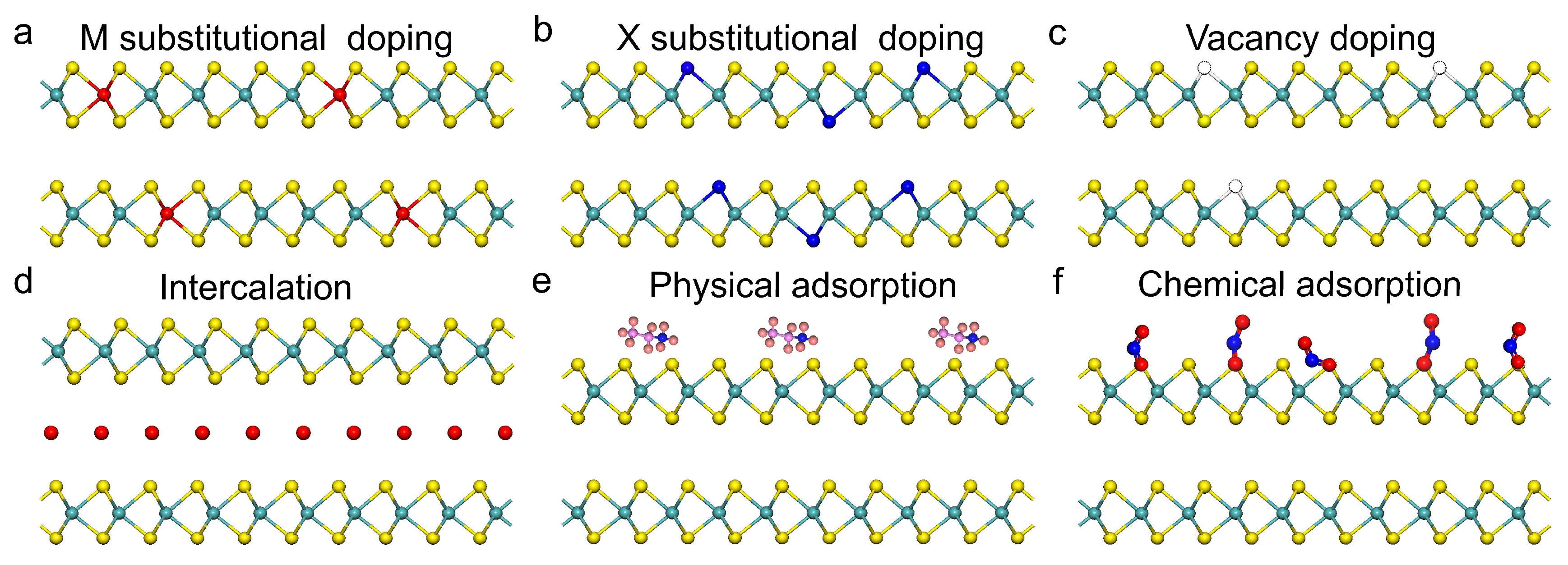
3.1. Substitutional Doping

Two-dimensional alloys have been reported early in MX2 (M = Mo, W, Re, Hf, Sn; X = S, Se, Te) [31,32,33,34,35,36,37,38,39,40,41,42,43,44,45,46,47,48]. It is a substitutional doping type and can be classified into a transition elements substitution (MxM’1-xX2, x represents the content of M) (Figure 2a) and chalcogenide elements substitution (MX2xX’2(1-x), x is the content of X) (Figure 2b). The doping concentration can be controlled by tuning the growth parameters, and the distribution of the doped atoms are random [33,49,50].

3.2. Vacancy

It is well known that vacancy defects either naturally formed or artificially made have a great influence on the electronic structure of 2DMs (Figure 2c). A theoretical calculation has shown that S vacancies in monolayer MoS2 will form donor-like levels and lead to n-type conductivities, while Mo vacancies bring acceptor-like levels and p-type conductivities [51]. Thus, vacancy is a common doping form and can determine the carrier type of 2D semiconductors.

3.3. Intercalation

The layers of 2DMs are combined by a van der Waals force. Therefore, the atoms and molecules can be inserted into the van der Waals layers by chemical methods [52]. These intercalated ones can change the electronic properties of the 2DMs, including the transformation of 2DMs from n-type to p-type [53], tuning the magnetic property [54,55], or bringing them into a phase transformation [56]. In our opinion, this intercalation should belong to the one of doping, and some of the doping will lead to a change in the space distance between the van der Waals layers (Figure 2d).

3.4. Adsorption

In addition to the atomic intercalation, the adsorption can also be an important doping type. When 2DMs exist in air or are specially treated, molecules and particles can adsorb on the surface of 2DMs. These molecules and particles will transfer the electron with 2DMs [57,58,59,60,61]. As the specific surface area of the 2DMs is large, the adsorption will seriously affect their electronic structure, thus we also classify this situation as a type of doping. Generally speaking, adsorption can be divided into two types: physical adsorption (Figure 2e) and chemical adsorption (Figure 2f). Physical adsorption refers to the formation of a van der Waals force between the adsorption and 2DMs, while the chemical adsorption means the formation of a covalent bond between the adsorption and 2DMs. In the experiment, we can choose different adsorbents to enhance their influence on 2DMs, which will affect the electrical transport and photoelectric properties of 2DMs [61].

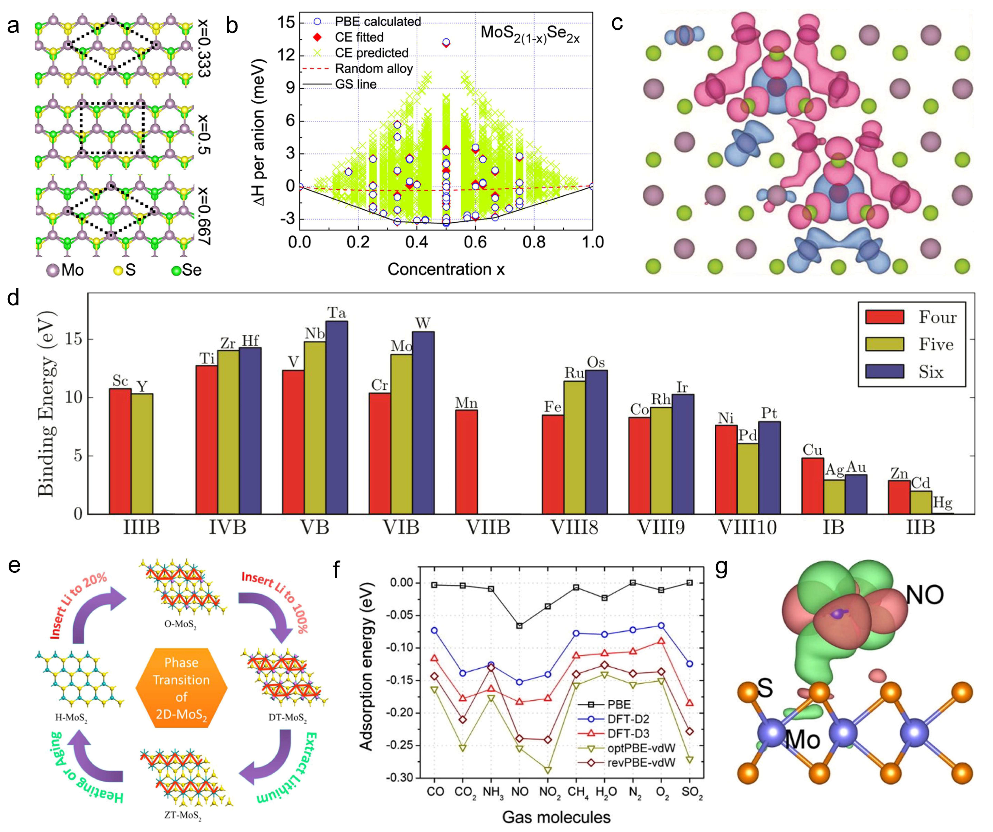
4. Theoretical Investigation of 2D Doped Materials

Up to now, researchers have studied the effects of various kinds of doping in 2DMs by a theoretical calculation, including substitutional doping, intercalation, and adsorption. A theoretical calculation can analyze the formation energy of the doping to determine the possibility of doping. At the same time, it can study the influence of doping on the band structure of 2D materials to predict the influence of doping on the electrical, optical, and magnetic properties of 2D materials. Compared with the experiment, the theoretical calculation is relatively simple, and the results obtained may not be completely consistent with the experimental results, but it will have a certain guiding significance for the experiment. Kang et al. investigated the stability of 2D alloys MX2(1-x)X’2x (M = Mo, W, and X, X’ = S, Se, Te) by employing the cluster expansion method and the special quasi-random structure approach (Figure 3a) [62]. The stability of the alloys at 0 K can be evaluated from their formation enthalpies (ΔH) which depends on the specific atomic arrangement in the alloys. The results show that for many configurations of this alloy, ΔH is negative, which means that the ordered alloy can form spontaneously (Figure 3b). There are three stable ground states, with concentration x equal to 1/3, 1/2, and 2/3 (Figure 3a). In these ground states, the clustering of the S or Se atoms is not stable, and the S (Se) atoms prefer to occupy the neighbor sites of the Se (S) atoms. These results show that the 2D alloy is thermally stable in theory [62]. Because of the high temperature in the synthesis of 2D alloys, it is difficult to observe the ordered situation in the experiment.
W atoms can be doped arbitrarily in MoS2 to form an alloy, while other metal atoms, such as Mn and Co, cannot be doped in a high concentration due to a lattice mismatch, thus only a small amount can be done. Cheng et al. investigated various atoms doped on the MoS2 monolayer by density functional theory [64]. To check the stability of different dopants, they have calculated the binding energies as summarized in Figure 3d. The binding energy is defined by the equation:
  E b = E v + μ E d
where Ev is the energy of a relaxed MoS2 monolayer with one Mo vacancy, μ is the energy of the doped transition metal atom, and Ed is the energy of a relaxed MoS2 monolayer with one Mo atom replaced by the transition metal. The result demonstrated that Eb of different dopants varies from 0.2 to 16.0 eV. The binding energy at IIIB to VIII10 is relatively high (Figure 3d). It is concluded that the substitution doping of the transition metal atoms from the IIIB to VIII 10 groups is stable [64]. Doping transition metal atoms from the IB and IIB groups is difficult because of their low binding energy (especially for Hg). For magnetic atoms, such as Mn, Fe, and Co, the doping of MoS2 can be a promising approach to achieve 2D diluted magnetic semiconductors [63,64,67,68]. Figure 3c shows the long-range interaction of MnMo defects through the Se 4p state in the spin-polar isosurface diagram [63]. Two MnMo defects were obtained, separated by a distance of ~6.5Å in MoSe2. The result shows that the coupling between the Mn spins and Se spins in the AFM resulted from the hybridization between the localized Mn 3d and the delocalized Se 4p states. More importantly, every time the Se spins come across a MnMo defect, the AFM alignment between the Se and Mn leads to an effective FM alignment of all the MnMo spins. Because the Se 4p states are delocalized, the FM alignment between the MnMo spins can also be expected to act over a long range. The ferromagnetism will be more stable and the Curie temperature will be higher with the increase in the Mn doping concentration [63].
It has been reported that the electronic and phase structure of 2DMs can be tuned by inserting atoms and ions into the van der Waals gap [69]. The mechanical exfoliation method always leads to a 2D trigonal prismatic phase (labeled as H-MoS2), which is found to be a semiconductor with a direct band gap between the occupied dz2 and the empty dx2−y2, xy orbitals [70]. The space group of the H-MoS2 phase is P6/mmc, which is considered to be a stable configuration under normal conditions [71]. However, the solvent-based exfoliation method results in different octahedral coordinated phases with each Mo atom bonded with six S atoms, which is referred to as T-MoS2 [72,73]. The structure of MoS2, which is similar to WTe2 with zigzag Mo−Mo chains rather than that of TiS2, is labeled as ZT-MoS2. Lithium-inserted MoS2 possesses a distorted octahedral coordinated structure with a rhombus shape connected Mo–Mo chains, which is referred to as DT-MoS2 [74]. O-MoS2 is used to describe all three octahedral coordinated MoS2 regardless of the detail of the molybdenum clusterization. M. Kan et al. discussed the possible transition paths of different phases of MoS2. As the concentration of the lithium atoms is increased, H-MoS2 becomes O-MoS2 and then becomes DT-MoS2. When all the Li atoms are extracted from the system, the structure is ZT-MoS2. By heating or aging, ZT-MoS2 will transform into the most stable phase H-MoS2 (Figure 3e) [65].
Up to now, MoS2 transistors have shown ultrahigh gas sensing capabilities for NO and NH3. This is mainly because the adsorbed gas changes the electronic structure of MoS2 by a charge transfer mechanism. The adsorption energy of various gas molecules on the MoS2 monolayer was determined by five methods (Figure 3f) [66]. For the same molecule, a different calculate method results in a different adsorption energy, while the trend of the adsorption energy is consistent with that of the gas molecules. The adsorption energy of NO2 and NO are high, which means that they can be easy to adsorb on MoS2 (Figure 3f). For all the molecules, no chemical bonding is found between the adsorbate and MoS2. To further elucidate the charge transfer between the gas adsorbate and the MoS2 monolayer, Figure 3g provides an isosurface map of the difference in the electron charge density of these gas molecules. There is a charge accumulation on the surface between the MoS2 and NO adsorbate, demonstrating the charge-donor characteristics of the molecules, which is also reflected by a high adsorption energy between them (Figure 3f) [66].

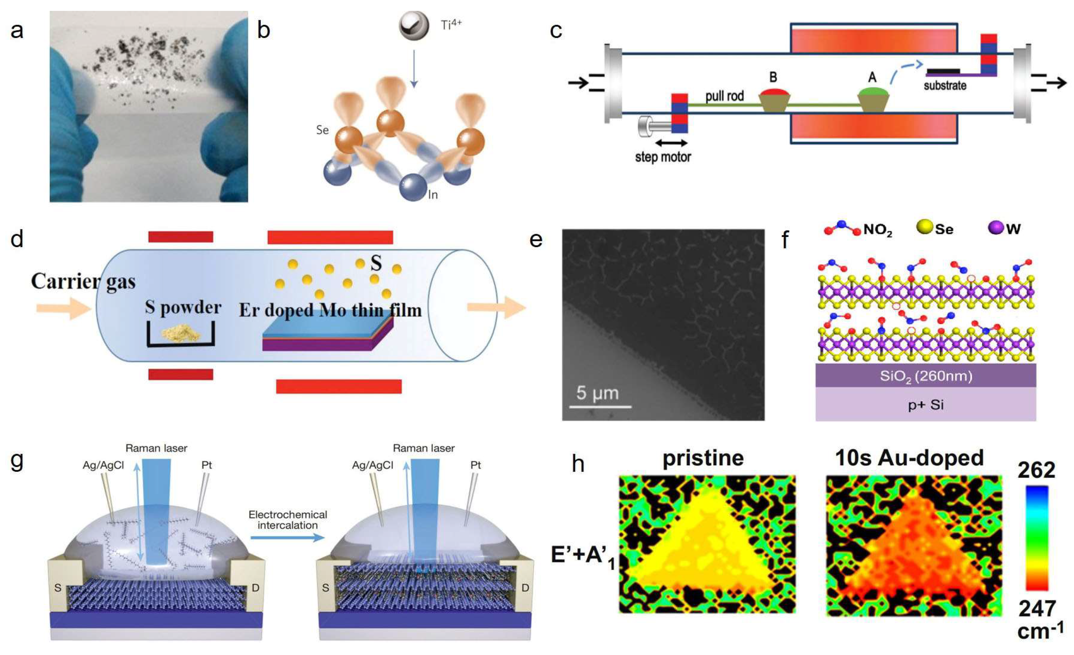
5. Synthesis of 2D Doped Materials

Compared with pure 2DMs, the synthesis of 2D doped materials is more challenging. Here, we summarized the methods to synthesize 2D doped materials, including a mechanical exfoliation, surface functionalization, vapor phase deposition, plasma technology, absorption, the electrochemical method, and thermal evaporation.

5.1. Mechanical Exfoliation Method

The mechanical exfoliation method was well known after graphene was exfoliated through tape in 2004 [1]. Because of the weak van der Waals force between the layers of layered materials, ultrathin and high-quality 2DMs can be obtained by this method (Figure 4a). The bulk counterparts of 2D doped crystals can be obtained by a chemical vapor transport (CVT) method where the source material is placed in the quartz tube by vacuum sealing technology and the samples are grown under an appropriate temperature. This method can obtain high-quality 2D substitution-doped materials with a low cost, but the layer thickness of 2D materials is uncontrollable, the efficiency is low, and large-scale production is difficult to achieve. Xie et al. have firstly exfoliated the Mo1−xWxS2 monolayer alloy from its bulk counterparts and shows its good optical performance [31].

5.2. Surface Functionalization

Surface functionalization is an adsorption-doped method and is possible to integrate various compositions of 2D functional units on single few-layered 2DMs. This method is simple to operate, but the stability needs to be improved because the dopants are on the surface and the interaction with the 2D materials is weak. Many 2DMs, such as MoS2, MoSe2, and InSe, have chalcogenide atoms with one bond occupied by lone pair electrons. According to the Pauli exclusion principle, the fully occupied orbital cannot accept extra electrons to form a chemical bond, resulting in an inert 2D surface. However, Lewis acids, featuring empty electron orbitals, can accept these lone pair electrons and form stable coordinate covalent bonds [75]. Ajayan et al. made use of the lone pair electrons found in most of 2D TMDCs and reported a functionalization method to tune their electronic transport via a Lewis acid–base reaction that does not alter the host structure (Figure 4b) [75].

5.3. Vapor Phase Deposition Method

Vapor phase deposition, including physical vapor deposition (PVD) and chemical vapor deposition (CVD), is a very common method to obtain 2D doped materials [21]. This method can control the thickness and size of 2D substitution-doped materials and can achieve the growth of large-area and high-quality 2D materials. Pan et al. developed a PVD method to grow a 2D alloy with a controlled concentration [76]. The precursor is usually the corresponding powder of a chalcogenide semiconductor. The two boats in the system are linked together and can be pushed optionally during the growth process. The vapor concentration of the two materials can be controlled precisely to modulate the chemical composition of the alloy [35,36,76]. Until now, there are mainly three CVD methods for synthesizing the 2D doped materials: (1) a direct synthesis from various source materials by a chemical reaction. In the synthesis of Co-doped MoS2, Co3O4, MoO3, and S are used as the source materials in a CVD system [81]. (2) Metal alloys were obtained by a vacuum evaporation on the substrate, and then vulcanized in the CVD system. Er-doped Mo thin films were deposited on SiO2/Si substrates by sputtering high purity Er and Mo targets with a different power to achieve Er doping into the films. Then, Er-doped MoS2 layered nanosheets were synthesized by the CVD method [77]. (3) The CVD approach combined with a solution-processed precursor deposition. The MoO3 and WO3 solution were prepared by adding MoO3 and WO3 powder into NH4OH and then annealed to form films, respectively. The films can be used as source materials to form a 2D alloy by the CVD approach [82].

5.4. Plasma Treatment

Plasma technology is used for doping 2DMs because of its simplicity and universality. It is well known that in chemically grown 2DMs, vacancy defects are particularly noticeable due to imperfections in the growth process. It is an effective approach to obtain 2DMs with a vacancy defect by an oxygen plasma exposure and hydrogen treatment (Figure 4e) [78]. Plasma can impact 2DMs to form vacancy defects, and H2 reacts with 2DMs to form a vacancy. The concentration of the vacancy increases with the increase in the dose and exposure time in the oxygen plasma’s exposure and temperature, and the hydrogen concentration in the hydrogen treatment [78].

5.5. Molecular Absorption Method

A molecular physical and chemical absorption method are extensively reported to achieve both n- and p-doping in 2DMs utilizing the surface charge transfer mechanisms which are aided. This method is simple to operate, but the stability needs to be improved because the dopants are on the surface and the interaction with the 2D materials is weak. Figure 4f shows that NO2 is located on WSe2 by physical and chemical absorption, and the sample is placed inside an evacuated Pyrex glass flask with an inert gas flow for the gas exchange [60,83]. Subsequently, a constant NO2 gas flow is introduced through the flask and maintained throughout the entire doping procedure, exhausting an external oil bath. Simultaneously, the flask is placed on a hot plate with the sample temperature maintained at a certain temperature and cooled down to room temperature [60].

5.6. Electrochemical Intercalation Method

Electrochemical intercalation has been recently used for doping 2DMs and obtaining a 2D superlattice. This method can obtain 2D intercalated materials with novel structures and physical properties, but it is difficult to achieve a mass preparation. Wang et al. used a home-designed electrochemical-optical measurement platform for the in situ monitoring of the intercalation dynamics and the corresponding evolution of the electronic and optical properties (Figure 4g) [79]. This method can be used for several different 2D atomic crystals, such as black phosphorus, molybdenum disulfide, and tungsten diselenide, to produce a broad class of superlattices with tailored molecular structures, interlayer distances, phase compositions, electronic, and optical properties [79].

5.7. Thermal Evaporation Method

The thermal evaporation method is carried out to product Au-decorated WSe2 with a p-type doping [80]. This method can achieve adsorption doping, but its ability to precisely control the physical properties is weak. A more p-type behavior of the decorated WSe2 field effect transistor is realized by the electron transfer from the WSe2 to the gold (Au) decorated on the WSe2 surfaces. This simple and scalable method is considered to be a promising method to introduce p-doping to other 2DMs (Figure 4h) [80].

6. Characterization of 2D Doped Materials

There are mainly seven methods to characterize 2D doped materials, including optical microscopy, X-ray photoelectron spectroscopy (XPS), X-ray diffraction (XRD), high angle annual dark field scanning transmission electron microscopy (HAADF-STEM), aberration-corrected transmission electron microscopy (TEM), and Raman and photoluminescence (PL) spectra.

6.1. Optical Microscopy

Two-dimensional doped materials with a different electronic structure and band gap may show a different color optical image. It is reported that the colors of Cu-SnS2 and Co-SnS2 become more opaque and turn dark blue and violet-red, respectively, from the light blue color of SnS2 (Figure 5a) [53].

6.2. Scanning Transmission Electron Microscopy

High angle annual dark field scanning transmission electron microscopy (HAADF-STEM) is one direct way to characterize the atomic arrangement in 2D substitution-doped materials, which has an atomic resolution and Z-contrast capability (contrast proportional to ~Z1.5−1.9) [86,87]. The HAADF-STEM image has been carried on 2D alloys [31,33,41,47,88,89], Mn-MoS2 [90], Fe-MoS2 [91], Fe-SnS2 [92], Nb-MoS2 [84], and Ti-InSe [75]. In the MoS2(1−x)Se2x alloy, the HAADF-STEM image is used to quantify the concentration of the Se local atom on the nanometer scale and map the atomic distribution of the Se dopants, where a single Se substitution site and a double substitution site are indicated in bright green and white, respectively (Figure 5b,c) [47].

6.3. Raman Spectroscopy

Raman spectroscopy has been widely used in 2D substitution-doped materials to characterize the phonon structure, including the crystallinity, composition, and doping. Modified random element isodisplacement (MREI) has been successfully used to explain the Raman behavior of the 2D alloys. The MREI model is based on the assumptions of isodisplacement and randomness: (1) the same kind of atoms vibrate in the same amplitude and phase and (2) all the substituted atoms are randomly distributed [32]. The MREI model can predict the mode behaviors and fit the composition-dependent Raman frequencies of A’1and E’ modes in a 2D alloy [32]. In the Raman spectra of Mo1-xWxSe2, when the W component x is increased from 0 to 1, the A1g mode continuously changes from 240.1 to 249.3 cm−1, which is close to the linear dependence on the W component (Figure 5d). In addition, as the W component changes, the second-order Raman peak also shifts and exhibits a dual-mode behavior [48]. The photoluminescence spectroscopy (PL) measurements are a non-destructive measurement method that quickly and easily characterizes the defects, impurities, and luminescence properties of 2DMs. In the PL spectrum of Mo1-xWxSe2, as the W component increases, the PL emission exhibits a bowing effect (Figure 5e). The emission energy is first red-shifted to a minimum at x = 0.2–0.3, and then monotonically blue-shifted [48].

6.4. X-ray Photoelectron Spectroscopy

XPS is an effective characterization for understanding the chemical states and composition of elements in 2D substitution-doped materials. The binding energy of the XPS spectra is referenced to the Fermi level in the material; the red/blue shifts of the binding energy can be interpreted by the move down/up of the Fermi level in the semiconductor, demonstrating p/n doping, respectively [93,94,95]. The XPS has been used to prove the doping concentration in Nb-MoS2 and it is found that the core-level peaks of Mo and S in the doped sample show a uniform shift toward the lower binding energies compared to those of the undoped one, demonstrating p doping (Figure 5f) [84].

6.5. Aberration-Corrected Transmission Electron Microscopy

Aberration-corrected transmission electron microscopy (TEM) is used to characterize the vacancy defect in 2DMs. A typical atomic image of a single-layer MoS2 showed the expected hexagonal symmetry, and the defects can be clearly distinguished by analyzing the intensity profile (Figure 5g) [85].

6.6. X-ray Diffraction Pattern

XRD is a powerful tool for analyzing the crystal structure of materials and is powerful to characterize 2D intercalated materials. The crystal plane spacing can be calculated from the XRD pattern by the Bragg equation. An intercalation in 2DMs will result in the increasing of the (001) crystal plane spacing, which can be characterized by XRD (Figure 5h) [79,96].

7. Properties and Applications of 2D Doped Materials

A wide variety of 2DMs have been used as the active material to fabricate field-effect transistors (FETs) [97,98,99], a photodetector [100], and hydrogen evolution catalysts [101]. Doping 2DMs can regulate their properties to meet the practical application [102]. We will focus on the applications of 2D doped materials in electrical, optoelectronic, catalytic, and magnetic fields.

7.1. Electrical Transport and Devices

To reduce the channel length in the current silicon-based transistor, the thickness of the semiconductor must also be reduced to ensure that 2D electrostatic screening effects are minimized [103]. Two-dimensional semiconductors with an atomic thickness are suitable for field effective transistors (FETs) because of their compatibility and the lack of short-channel effects. The mobility (μ) and current ON/OFF ratio (ION/IOFF) are performance indicators of FETs. μ is an important physical parameter to indicate the speed of the carrier electron movement under an electric field. A high mobility can reduce the power consumption of devices and improve the current carrying capacity and operating frequency of devices. The mobility is decided by the mean-free time (τ) and effective mass (m*) of the electron as follows:
μ = q τ m *
where m* is related to the band structure. Because doping tends to increase the scattering and τ, it is a feasible method to reduce the effective quality by selecting specific dopants. On the other hand, doping can also achieve a low contact resistance and improve the mobility of 2DMs by adjusting the Fermi energy level to adjust the work function.
A large ON/OFF ratio can contribute to a reduced power dissipation and static leakage current. The ON current (ION) is related to the carrier mobility, saturation velocity, and metal–semiconductor contact resistance, and has no direct relation with the bandgap [104]. The OFF current (IOFF) of the transistor is strongly dependent on the bandgap (Eg), according to the equation:
I OFF e x p E g α K T
where K is the Boltzmann constant, T is the temperature, and α is a constant.
Doping can change the band’s structure and affect the electrical properties of 2DMs. In a typical n-type 2D semiconductor, doping can introduce more electrons or holes, resulting in the Fermi level closing to the conduction band or valence band (Figure 6a). It can even turn an n-type semiconductor into a p-type. So, more n-type and p-type materials can be obtained by doping, which is the cornerstone of the whole integrated circuit. There are some doping methods to control the conductive type of 2D semiconductors: substitution, surface functionalization, and intercalation.
Natural MoS2 show n-type. Niobium (Nb) has one less valence electron than Mo and is suggested as the suitable acceptor [106]. It was reported that 0.5%Nb substitutional doped MoS2 show p-type with a degenerate hole density of ~3 × 1019 cm−3 (Figure 6b) [84]. Two-dimensional TMDs have a van der Waals gap between two neighboring chalcogenide atoms layers and the chalcogen ions on the 2D surfaces are capped with lone pair electron orbitals [75]. On the basis of the Pauli exclusion principle, the fully occupied orbital cannot accept extra electrons to form a chemical bond, resulting in an inert 2D surface. However, Lewis acids (e.g., TiCl4), possessing empty electron orbitals of the metallic ions, can accept these lone pair electrons of chalcogenide atoms and form stable coordinate covalent bonds [75]. Thus, some n-type 2D semiconductors can be changed into the p-type by the surface functionalization doping method via a Lewis acid–base reaction (Figure 6c) [76]. There are van der Waal gaps in 2D layered materials, and heteroatom can be intercalated into the gap by a solvent-based method. The electrons of intercalated heteroatom will couple with those of 2DMs, thus changing the band structure of the 2DMs. Gong et al. reported that pristine bilayer SnS2 show the n-type, the Cu intercalated bilayer SnS2 displays a hole field-effect mobility of ~40 cm2 V−1 s−1, and the Co intercalated bilayer SnS2 exhibits a metal behavior with a sheet resistance comparable to that of few-layer graphene (Figure 6d) [53]. Chalcogenide atoms in 2D TMD can easily form vacancies, which can be occupied by a molecular doping. A new type of 2D doped material, such as Cl-doped MoS2 (Figure 6e), can shorten the width of the Schottky barrier between MoS2 and metal, and thus reduce its contact resistance (Figure 6f) [61]. The 2D vertical superlattice can be formed by inserting organic molecules into 2DMs by the electrochemical method [107]; it can increase the interlayer spacing and change the electronic structure of materials and make the multi-layer 2DMs exhibit single-layer properties (Figure 6g). At the same time, the stability of 2DMs in air can be improved (Figure 6h) [79]. The electronic structure of 2DMs can be changed by the charge transfer between the organic compound and 2DMs by placing some electron donor organic compound on the surface of 2DMs by chemical method. When benzyl viologen (BV), one of the highest reduction potentials of all electron donor organic compounds, as a surface charge transfer donor for MoS2 flakes can obtain a high electron sheet density of ~1.2 × 1013 cm−2, which corresponds to the degenerate doping limit for MoS2 (Figure 6i) [105].

7.2. Optoelectronics, Catalysis and Magnetism

In an optoelectronic device based on 2DMs, the photocurrent (Iph) is defined by the equation:
  I p h = ( P e t α h v ) τ l / τ t
where P is the incident power, e is the electron charge, t is the thickness of 2DMs, α is the absorption coefficient of 2DMs at the photon energy hv, τl is the minority carrier lifetime, and τt is the transit time of the electron in 2DMs. The photoresponsivity R of the device can be described by the equation:
R = I p h / P = ( e t α h v ) τ l / τ t
When the illumination reaches the sample, the electron–hole pairs are generated [108,109]. The photoconductivity is enhanced by decreasing the recombination of these electron–hole pairs via the trap states to capture the minority carriers to prolong their τl, and at the same time, most carriers are allowed to transmit effectively multiple times over the channel between the source and drain the electrode.
Doping often leads to an increase in the defects in 2DMs, which leads to the increase in the trapped states in the band structures, τl, and the photoresponsivity [110,111,112]. On the other hand, the defect trap states will prolong the photo response time. Doping can lead to the introduction of impurity levels or a changing of the band structure, which can improve the optical absorption coefficient. Two-dimensional SnSSe as a phototransistor is demonstrated to exhibit a high photoresponsivity of about 6000 A W−1 due to the presence of Van Hove singularities in the band structure introduced by doping (Figure 7a) [44]. CoMoS and NiMoS formed by Co and Ni doping MoS2 have excellent hydrogen evolution reaction (HER) performances. For an HER, the catalytic performance is closely related to the adsorption energy of hydrogen and the kinetic energy barrier of the hydrogen generation pathway. The introduction of a foreign metal element (e.g., Co, Ni, or Fe) in the MoS2 lattice affords the opportunity to engineer the electronic and/or surface structures for improving the HERs performances. The optimized Co-doped MoS2 catalyst shows a superior HER performance with a high exchange current density of 0.03 mA·cm−2, a low onset potential of 90 mV, and a small Tafel slope of 50 mV·dec−1, which also exhibits the excellent stability of 10,000 cycles with a negligible loss of the cathodic current (Figure 7b) [113]. Lithium intercalation in 2D layered materials can be used to tune the phase. The 2H-1T phase of MoS2 transform during the intercalation reaction, which is driven by an electron transfer from Li to MoS2, causing a change in the electron count from d2 to d3, leading to the destabilization of the original crystal structure [114]. The plasma-assisted approach (SF6, CHF3, CF4, and O2 plasmas) is an effective method to make a change from n-type MoS2 to p-type MoS2 by doping (Figure 7d). Because of the relatively strong electronegativity of the F and O atoms, the excess electrons are preferentially transferred from the MoS2 layers onto the F and O atoms, resulting in p-doping in the MoS2 layers [115,116,117]. Charge doping is used to tune the phase of TMDs by modulating the Fermi level and changing the electronic properties. The excitation of the plasmon modes in Au nanoparticles deposited on a MoS2 monolayer may induce a transient reversible 2H to 1T phase transition in MoS2 by hot electron doping (Figure 7e). The doping of the 2H phase first leads to the destabilization of the lattice, and then, through the population of the Mo 4d orbitals, into a structural transition to the 1T phase. The Raman spectra taken with and without Au NPs further confirms this phase transition (Figure 7f) [118]. The magnetic atoms doped in TMDs may induce a ferromagnetism by p–d antiferromagnetic coupling (Figure 7g). It is reported that undoped SnS2 show no magnetism (Figure 7h), but Fe-doped SnS2 with a Curie temperature of 31 K show a ferromagnetism under 2 K (Figure 7i) [92,119].

8. Conclusions and Outlook

Doping is an important technology in the field of semiconductor science, which is also very important for the future device application research of 2DMs. In this review, we systematically introduced 2D doped materials, including various doping types and theoretical calculations, preparation and characterization methods, and a multifunctional application.
Although in the past few years great progress has been achieved in the field of 2D doped materials, there still exist a number of significant issues that need to be addressed and studied. First, the device size of 2DMs will continue to shrink, and the doped atoms will have a great impact on the device’s performance. Therefore, it is urgent to develop a 2DM doping method with a large-scale, universal, and atomic accurate. Second, the electrical, optoelectronic, catalytic, and magnetic properties of 2DMs have been widely studied. How to select appropriate doped atoms to significantly improve these performance needs further research, including theoretical and experimental research. Third, most of the 2D doped materials are still focused on basic research. In order to further promote their practical application, they need to be constructed into multi-functional devices, such as the p-n junction formed by 2D p-type doped and n-type doped materials, and magnetic doped semiconductors used in semiconductor spintronic devices.

Author Contributions

Conceptualization, J.L. and B.L.; methodology, J.L.; software, B.L. and Q.L.; validation, J.L., B.L. and Q.L.; formal analysis, B.L. and Q.L.; investigation, J.L. and B.L.; resources, B.L. and Q.L.; data curation, J.L.; writing—original draft preparation, J.L. All authors have read and agreed to the published version of the manuscript.

Funding

This work was supported by the National Natural Science Foundation of China (Grant No. 62174051), the Natural Science Foundation of Hunan Province (Grant No. 2022JJ10022), the Hunan Province “Huxiang Talents” Project (Grant No. 2021RC3038), and the Shenzhen Basic Research Project (Grant No. JCYJ20210324142012035), Natural Science Foundation of Chongqing, China (Grant No. cstc2021jcyj-msxmX0126).

Institutional Review Board Statement

Not applicable.

Informed Consent Statement

Not applicable.

Conflicts of Interest

The authors declare no conflict of interest.

References

  1. Novoselov, K.S.; Geim, A.K.; Morozov, S.V.; Jiang, D.; Zhang, Y.; Dubonos, S.V.; Grigorieva, I.V.; Firsov, A.A. Electric Field Effect in Atomically Thin Carbon Films. Science 2004, 306, 666–669. [Google Scholar] [CrossRef] [PubMed] [Green Version]
  2. Zhao, B.; Wan, Z.; Liu, Y.; Xu, J.; Yang, X.; Shen, D.; Zhang, Z.; Guo, C.; Qian, Q.; Li, J.; et al. High-order superlattices by rolling up van der Waals heterostructures. Nature 2021, 591, 385–390. [Google Scholar] [CrossRef] [PubMed]
  3. Wang, D.; Zhang, Z.; Li, B.; Duan, X. Synthesis of two-dimensional/one-dimensional heterostructures with tunable width. J. Semicond. 2021, 42, 092001. [Google Scholar] [CrossRef]
  4. Li, J.; Liang, J.; Yang, X.; Li, X.; Zhao, B.; Li, B.; Duan, X. Controllable Preparation of 2D Vertical van der Waals Heterostructures and Superlattices for Functional Applications. Small 2022, 18, 2107059. [Google Scholar] [CrossRef]
  5. Zhang, Y.; Wang, Z.; Feng, J.; Ming, S.; Qu, F.; Xia, Y.; He, M.; Hu, Z.; Wang, J. Synthesis and electromagnetic transport of large-area 2D WTe2 thin film. J. Semicond. 2022, 43, 102002. [Google Scholar] [CrossRef]
  6. Qin, B.; Ma, H.; Hossain, M.; Zhong, M.; Xia, Q.; Li, B.; Duan, X. Substrates in the Synthesis of Two-Dimensional Materials via Chemical Vapor Deposition. Chem. Mater 2020, 32, 10321–10347. [Google Scholar] [CrossRef]
  7. Yuan, P.; Zhang, T.; Sun, J.; Liu, L.; Yao, Y.; Wang, Y. Recent progress in 2D group-V elemental monolayers: Fabrications and properties. J. Semicond. 2020, 41, 081003. [Google Scholar] [CrossRef]
  8. Li, B.; Wan, Z.; Wang, C.; Chen, P.; Huang, B.; Cheng, X.; Qian, Q.; Li, J.; Zhang, Z.; Sun, G.; et al. Van der Waals epitaxial growth of air-stable CrSe2 nanosheets with thickness-tunable magnetic order. Nat. Mater. 2021, 20, 818–825. [Google Scholar] [CrossRef]
  9. Li, Z.; Shu, W.; Li, Q.; Xu, W.; Zhang, Z.; Li, J.; Wang, Y.; Liu, Y.; Yang, J.; Chen, K.; et al. Nondegenerate P-Type In-Doped SnS2 Monolayer Transistor. Adv. Electron. Mater. 2021, 7, 2001168. [Google Scholar] [CrossRef]
  10. Li, B.; Deng, X.; Shu, W.; Cheng, X.; Qian, Q.; Wan, Z.; Zhao, B.; Shen, X.; Wu, R.; Shi, S.; et al. Air-stable ultrathin Cr3Te4 nanosheets with thickness-dependent magnetic biskyrmions. Mater. Today 2022, 57, 66–74. [Google Scholar] [CrossRef]
  11. Zhao, D.; Zhang, C.; Zhang, C.; Ji, W.; Li, S.; Wang, P. Magnetic tuning in a novel half-metallic Ir2TeI2 monolayer. J. Semicond. 2022, 43, 052001. [Google Scholar] [CrossRef]
  12. Mounet, N.; Gibertini, M.; Schwaller, P.; Campi, D.; Merkys, A.; Marrazzo, A.; Sohier, T.; Castelli, I.E.; Cepellotti, A.; Pizzi, G.; et al. Two-dimensional materials from high-throughput computational exfoliation of experimentally known compounds. Nat. Nanotechnol. 2018, 13, 246–252. [Google Scholar] [CrossRef] [Green Version]
  13. Chang, C.; Chen, W.; Chen, Y.; Chen, Y.; Chen, Y.; Ding, F.; Fan, C.; Jin Fan, H.; Fan, Z.; Gong, C.; et al. Recent Progress on Two-Dimensional Materials. Acta Phys-Chim. Sin. 2021, 37, 2108017. [Google Scholar] [CrossRef]
  14. Liu, W.; Bao, H.; Li, Y.; Ma, F. Highly tunable electronic structure and linear dichroism in 90 degrees twisted alpha-phosphorus carbide bilayer: A first-principles calculation. Phys. Chem. Chem. Phys. 2021, 23, 7080–7087. [Google Scholar] [CrossRef]
  15. Xiang, Y.; Xia, Q.-l.; Luo, J.-h.; Liu, Y.-p.; Peng, Y.-d.; Wang, D.-w.; Nie, Y.-z.; Guo, G.-h. Observation of ferromagnetism in black phosphorus nanosheets with high magnetization by liquid exfoliation. Solid State Commun. 2018, 281, 1–5. [Google Scholar] [CrossRef]
  16. Shi, S.; Feng, Y.; Li, B.; Zhang, H.; Li, Q.; Mo, Z.; Zhou, X.; Lu, Z.; Dang, W.; Lin, X.; et al. Broadband and high-performance SnS2/FePS3/graphene van der Waals heterojunction photodetector. Appl. Phys. Lett. 2022, 120, 081101. [Google Scholar] [CrossRef]
  17. Liu, Y.; Weiss, N.O.; Duan, X.; Cheng, H.-C.; Huang, Y.; Duan, X. Van der Waals heterostructures and devices. Nat. Rev. Mater. 2016, 1, 16042. [Google Scholar] [CrossRef]
  18. Wang, X.; Pan, L.; Yang, J.; Li, B.; Liu, Y.Y.; Wei, Z. Direct Synthesis and Enhanced Rectification of Alloy-to-Alloy 2D Type-II MoS2(1-x)Se2x/SnS2(1-y)Se2y Heterostructures. Adv. Mater. 2021, 33, e2006908. [Google Scholar] [CrossRef]
  19. Wang, P.; Han, S.; Quhe, R. Quantum transport simulation of the two-dimensional GaSb transistors. J. Semicond. 2021, 42, 122001. [Google Scholar] [CrossRef]
  20. Huang, M.; Zheng, Z.; Dai, Z.; Guo, X.; Wang, S.; Jiang, L.; Wei, J.; Chen, S. DASP: Defect and Dopant ab-initio Simulation Package. J. Semicond. 2022, 43, 042101. [Google Scholar] [CrossRef]
  21. Zhou, X.; Liu, C.; Song, L.; Zhang, H.; Huang, Z.; He, C.; Li, B.; Lin, X.; Zhang, Z.; Shi, S.; et al. Promoting the optoelectronic and ferromagnetic properties of Cr2S3 nanosheets via Se doping. Sci. China Phys. Mech. 2022, 65, 276811. [Google Scholar] [CrossRef]
  22. Zhu, H.; Gan, X.; McCreary, A.; Lv, R.; Lin, Z.; Terrones, M. Heteroatom doping of two-dimensional materials: From graphene to chalcogenides. Nano Today 2020, 30, 100829. [Google Scholar] [CrossRef]
  23. Wang, Y.; Zheng, Y.; Han, C.; Chen, W. Surface charge transfer doping for two-dimensional semiconductor-based electronic and optoelectronic devices. Nano Res. 2020, 14, 1682–1697. [Google Scholar] [CrossRef]
  24. Loh, L.; Zhang, Z.; Bosman, M.; Eda, G. Substitutional doping in 2D transition metal dichalcogenides. Nano Res. 2021, 14, 1668–1681. [Google Scholar] [CrossRef]
  25. Rana, F.; Koksal, O.; Jung, M.; Shvets, G.; Vamivakas, A.N.; Manolatou, C. Exciton-Trion Polaritons in Doped Two-Dimensional Semiconductors. Phys. Rev. Lett. 2021, 126, 127402. [Google Scholar] [CrossRef]
  26. Shen, D.; Zhao, B.; Zhang, Z.; Zhang, H.; Yang, X.; Huang, Z.; Li, B.; Song, R.; Jin, Y.; Wu, R.; et al. Synthesis of Group VIII Magnetic Transition-Metal-Doped Monolayer MoSe2. ACS Nano 2022, 16, 10623–10631. [Google Scholar] [CrossRef]
  27. Luo, J.-H.; Li, B.; Zhang, J.-M.; Zhong, M.-Z.; Xia, Q.-L.; Nie, Y.-Z.; Guo, G.-H. Bi doping-induced ferromagnetism of layered material SnSe2 with extremely large coercivity. J. Magn. Magn. Mater. 2019, 486, 165269. [Google Scholar] [CrossRef]
  28. Xin, K.; Wang, X.; Grove-Rasmussen, K.; Wei, Z. Twist-angle two-dimensional superlattices and their application in (opto)electronics. J. Semicond. 2022, 43, 011001. [Google Scholar] [CrossRef]
  29. Shen, G.; Zhao, Y.; Bai, Y.; Liu, J.; Xie, H.; Dong, Z.; Yang, J.; Yu, D. Photoluminescene study acceptor defects in lightly doped n type GaSb single crystals. J. Semicond. 2019, 40, 042101. [Google Scholar] [CrossRef]
  30. Sze, S.M.; Lee, M.-K. Semiconductor Devices: Physics and Technology, 3rd ed.; John Wiley & Sons: Hoboken, NJ, USA, 2012; p. 592. [Google Scholar]
  31. Chen, Y.; Xi, J.; Dumcenco, D.O.; Liu, Z.; Suenaga, K.; Wang, D.; Shuai, Z.; Huang, Y.-S.; Xie, L. Tunable band gap photoluminescence from atomically thin transition-metal dichalcogenide alloys. ACS Nano 2013, 7, 4610–4616. [Google Scholar] [CrossRef]
  32. Chen, Y.; Dumcenco, D.O.; Zhu, Y.; Zhang, X.; Mao, N.; Feng, Q.; Zhang, M.; Zhang, J.; Tan, P.-H.; Huang, Y.-S.; et al. Composition-dependent Raman modes of Mo1-xWxS2 monolayer alloys. Nanoscale 2014, 6, 2833–2839. [Google Scholar] [CrossRef] [PubMed] [Green Version]
  33. Qingliang, F.; Yiming, Z.; Jinhua, H.; Mei, Z.; Wenjie, D.; Nannan, M.; Juanxia, W.; Hua, X.; Fengliang, D.; Fang, L.; et al. Growth of large-area 2D MoS2(1-x)Se2x semiconductor alloys. Adv. Mater. 2014, 26, 2648–2653. [Google Scholar]
  34. Feng, Q.; Mao, N.; Wu, J.; Xu, H.; Wang, C.; Zhang, J.; Xie, L. Growth of MoS2(1-x)Se2x (x = 0.41–1.00) monolayer alloys with controlled morphology by physical vapor deposition. ACS Nano 2015, 9, 7450–7455. [Google Scholar] [CrossRef]
  35. Li, H.; Duan, X.; Wu, X.; Zhuang, X.; Zhou, H.; Zhang, Q.; Zhu, X.; Hu, W.; Ren, P.; Guo, P.; et al. Growth of alloy MoS2xSe2(1–x) nanosheets with fully tunable chemical compositions and optical properties. J. Am. Chem. Soc. 2014, 136, 3756–3759. [Google Scholar] [CrossRef] [PubMed]
  36. Li, H.; Zhang, Q.; Duan, X.; Wu, X.; Fan, X.; Zhu, X.; Zhuang, X.; Hu, W.; Zhou, H.; Pan, A.; et al. Lateral growth of composition graded atomic layer MoS2(1-x)Se2x nanosheets. J. Am. Chem. Soc. 2015, 137, 5284–5287. [Google Scholar] [CrossRef] [PubMed]
  37. Duan, X.; Wang, C.; Fan, Z.; Hao, G.; Kou, L.; Halim, U.; Li, H.; Wu, X.; Wang, Y.; Jiang, J.; et al. Synthesis of WS2xSe2–2x Alloy Nanosheets with Composition-Tunable Electronic Properties. Nano Lett. 2016, 16, 264–269. [Google Scholar] [CrossRef]
  38. Mann, J.; Ma, Q.; Odenthal, P.M.; Isarraraz, M.; Le, D.; Preciado, E.; Barroso, D.; Yamaguchi, K.; von Son Palacio, G.; Nguyen, A.; et al. 2-dimensional transition metal dichalcogenides with tunable direct band gaps: MoS2(1–x)Se2x monolayers. Adv. Mater. 2014, 26, 1399–1404. [Google Scholar] [CrossRef]
  39. Dou, C.X.; Wen, W.; Wang, J.L.; Ma, M.Y.; Xie, L.M.; Ho, C.H.; Wei, Z.Y. Ternary ReS2(1-x)Se2x alloy saturable absorber for passively Q-switched and mode-locked erbium-doped all-fiber lasers. Photonics Res. 2019, 7, 283–288. [Google Scholar] [CrossRef]
  40. Yu, P.; Lin, J.; Sun, L.; Le, Q.L.; Yu, X.; Gao, G.; Hsu, C.-H.; Wu, D.; Chang, T.-R.; Zeng, Q.; et al. Metal–semiconductor phase-transition in WSe2(1-x)Te2x monolayer. Adv. Mater. 2017, 29, 1603991. [Google Scholar] [CrossRef]
  41. Song, J.-G.; Ryu, G.H.; Lee, S.J.; Sim, S.; Lee, C.W.; Choi, T.; Jung, H.; Kim, Y.; Lee, Z.; Myoung, J.-M.; et al. Controllable synthesis of molybdenum tungsten disulfide alloy for vertically composition-controlled multilayer. Nat. Commun. 2015, 6, 7817. [Google Scholar] [CrossRef] [Green Version]
  42. Kudrynskyi, Z.R.; Wang, X.; Sutcliffe, J.; Bhuiyan, M.A.; Fu, Y.; Yang, Z.; Makarovsky, O.; Eaves, L.; Solomon, A.; Maslyuk, V.T.; et al. Van der Waals SnSe2(1−x)S2x alloys: Composition-dependent bowing coefficient and electron–phonon interaction. Adv. Funct. Mater. 2020, 30, 1908092. [Google Scholar] [CrossRef]
  43. Wang, Y.; Huang, L.; Li, B.; Shang, J.; Xia, C.; Fan, C.; Deng, H.-X.; Wei, Z.; Li, J. Composition-tunable 2D SnSe2(1-x)S2x alloys towards efficient bandgap engineering and high performance (opto) electronics. J. Mater. Chem. C 2017, 5, 84–90. [Google Scholar] [CrossRef]
  44. Perumal, P.; Ulaganathan, R.K.; Sankar, R.; Liao, Y.-M.; Sun, T.-M.; Chu, M.-W.; Chou, F.C.; Chen, Y.-T.; Shih, M.-H.; Chen, Y.-F. Ultra-thin layered ternary single crystals Sn(SxSe1-x)2 with bandgap engineering for high performance phototransistors on versatile substrates. Adv. Funct. Mater. 2016, 26, 3630–3638. [Google Scholar] [CrossRef]
  45. Liu, H.; Antwi, K.K.A.; Chua, S.; Chi, D. Vapor-phase growth and characterization of Mo1-xWxS2 (0 < x < 1) atomic layers on 2-inch sapphire substrates. Nanoscale 2014, 6, 624–629. [Google Scholar] [PubMed]
  46. Tongay, S.; Narang, D.S.; Kang, J.; Fan, W.; Ko, C.; Luce, A.V.; Wang, K.X.; Suh, J.; Patel, K.D.; Pathak, V.M.; et al. Two-dimensional semiconductor alloys: Monolayer Mo1-xWxSe2. Appl. Phys. Lett. 2014, 104, 012101. [Google Scholar] [CrossRef] [Green Version]
  47. Gong, Y.; Liu, Z.; Lupini, A.R.; Shi, G.; Lin, J.; Najmaei, S.; Lin, Z.; Elias, A.L.; Berkdemir, A.; You, G.; et al. Band gap engineering and layer-by-layer mapping of selenium-doped molybdenum disulfide. Nano Lett. 2014, 14, 442–449. [Google Scholar] [CrossRef] [PubMed]
  48. Zhang, M.; Wu, X.J.; Zhu, X.Y.; Dumcenco, X.D.O.; Hong, J.; Mao, N.; Deng, S.; Chen, Y.; Yang, Y.; Jin, C.; et al. Two-Dimensional Molybdenum Tungsten Diselenide Alloys: Photoluminescence, Raman Scattering, and Electrical Transport. ACS Nano 2014, 8, 7130–7137. [Google Scholar] [CrossRef] [PubMed]
  49. Xie, L. Two-dimensional transition metal dichalcogenide alloys: Preparation, characterization and applications. Nanoscale 2015, 7, 18392–18401. [Google Scholar] [CrossRef]
  50. Liang, F.; Xu, H.; Dong, Z.; Xie, Y.; Luo, C.; Xia, Y.; Zhang, J.; Wang, J.; Wu, X. Substrates and interlayer coupling effects on Mo1−xWxSe2 alloys. J. Semicond. 2019, 40, 062005. [Google Scholar] [CrossRef]
  51. Feng, L.P.; Su, J.; Liu, Z.T. Effect of vacancies on structural, electronic and optical properties of monolayer MoS2: A first-principles study. J. Alloy Compd. 2014, 613, 122–127. [Google Scholar] [CrossRef]
  52. Zhou, X.; Yang, J.; Zhong, M.; Xia, Q.; Li, B.; Duan, X.; Wei, Z. Intercalation of Two-dimensional Layered Materials. Chem. Res. Chin. Univ. 2020, 36, 584–596. [Google Scholar] [CrossRef]
  53. Gong, Y.; Yuan, H.; Wu, C.L.; Tang, P.; Yang, S.Z.; Yang, A.; Li, G.; Liu, B.; van de Groep, J.; Brongersma, M.L.; et al. Spatially controlled doping of two-dimensional SnS2 through intercalation for electronics. Nat. Nanotechnol. 2018, 13, 294–299. [Google Scholar] [CrossRef] [PubMed]
  54. Miao, Y.-Q.; Guo, J.-J.; Luo, Z.-Y.; Zhong, M.-Z.; Li, B.; Wang, X.-G.; Nie, Y.-Z.; Xia, Q.-L.; Guo, G.-H. Anisotropic Magnetoresistance Effect of Intercalated Ferromagnet FeTa3S6. Front. Phys. 2022, 10, 847402. [Google Scholar] [CrossRef]
  55. Qi, B.-T.; Guo, J.-J.; Miao, Y.-Q.; Zhong, M.-Z.; Li, B.; Luo, Z.-Y.; Wang, X.-G.; Nie, Y.-Z.; Xia, Q.-L.; Guo, G.-H. Abnormal Magnetoresistance Transport Properties of van der Waals Antiferromagnetic FeNbTe2. Front. Phys. 2022, 10, 851838. [Google Scholar] [CrossRef]
  56. Guo, Y.; Sun, D.; Ouyang, B.; Raja, A.; Song, J.; Heinz, T.F.; Brus, L.E. Probing the dynamics of the metallic-to-semiconducting structural phase transformation in MoS2 crystals. Nano Lett. 2015, 15, 5081–5088. [Google Scholar] [CrossRef]
  57. Tongay, S.; Zhou, J.; Ataca, C.; Liu, J.; Kang, J.S.; Matthews, T.S.; You, L.; Li, J.; Grossman, J.C.; Wu, J. Broad-range modulation of light emission in two-dimensional semiconductors by molecular physisorption gating. Nano Lett. 2013, 13, 2831–2836. [Google Scholar] [CrossRef] [PubMed]
  58. Sarkar, D.; Xie, X.; Kang, J.; Zhang, H.; Liu, W.; Navarrete, J.; Moskovits, M.; Banerjee, K. Functionalization of transition metal dichalcogenides with metallic nanoparticles: Implications for doping and gas-sensing. Nano Lett. 2015, 15, 2852–2862. [Google Scholar] [CrossRef]
  59. Kang, D.-H.; Shim, J.; Jang, S.K.; Jeon, J.; Jeon, M.H.; Yeom, G.Y.; Jung, W.-S.; Jang, Y.H.; Lee, S.; Park, J.-H. Controllable nondegenerate p-type doping of tungsten diselenide by octadecyltrichlorosilane. ACS Nano 2015, 9, 1099–1107. [Google Scholar] [CrossRef]
  60. Zhao, P.; Kiriya, D.; Azcatl, A.; Zhang, C.; Tosun, M.; Liu, Y.-S.; Hettick, M.; Kang, J.S.; McDonnell, S.; KC, S.; et al. Air Stable p-Doping of WSe2 by Covalent Functionalization. ACS Nano 2014, 8, 10808–10814. [Google Scholar] [CrossRef]
  61. Yang, L.; Majumdar, K.; Liu, H.; Du, Y.; Wu, H.; Hatzistergos, M.; Hung, P.Y.; Tieckelmann, R.; Tsai, W.; Hobbs, C.; et al. Chloride molecular doping technique on 2D materials: WS2 and MoS2. Nano Lett. 2014, 14, 6275–6280. [Google Scholar] [CrossRef] [Green Version]
  62. Kang, J.; Tongay, S.; Li, J.; Wu, J. Monolayer semiconducting transition metal dichalcogenide alloys: Stability and band bowing. J. Appl. Phys. 2013, 113, 143703. [Google Scholar] [CrossRef]
  63. Mishra, R.; Zhou, W.; Pennycook, S.J.; Pantelides, S.T.; Idrobo, J.-C. Long-range ferromagnetic ordering in manganese-doped two-dimensional dichalcogenides. Phys. Rev. B 2013, 88, 144409. [Google Scholar] [CrossRef]
  64. Cheng, Y.C.; Zhu, Z.Y.; Mi, W.B.; Guo, Z.B.; Schwingenschlögl, U. Prediction of two-dimensional diluted magnetic semiconductors: Doped monolayer MoS2 systems. Phys. Rev. B 2013, 87, 100401. [Google Scholar] [CrossRef] [Green Version]
  65. Kan, M.; Wang, J.Y.; Li, X.W.; Zhang, S.H.; Li, Y.W.; Kawazoe, Y.; Sun, Q.; Jena, P. Structures and Phase Transition of a MoS2 Monolayer. J. Phys. Chem. C 2014, 118, 1515–1522. [Google Scholar] [CrossRef]
  66. Zhao, S.; Xue, J.; Kang, W. Gas adsorption on MoS2 monolayer from first-principles calculations. Chem. Phys. Lett. 2014, 595–596, 35–42. [Google Scholar] [CrossRef] [Green Version]
  67. Ramasubramaniam, A.; Naveh, D. Mn-doped monolayer MoS2: An atomically thin dilute magnetic semiconductor. Phys. Rev. B 2013, 87, 195201. [Google Scholar] [CrossRef]
  68. Singh, N.; Schwingenschlogl, U. A Route to Permanent Valley Polarization in Monolayer MoS2. Adv. Mater. 2017, 29, 1600970. [Google Scholar] [CrossRef]
  69. Li, Q.-Q.; Li, S.; Wu, D.; Ding, Z.-K.; Cao, X.-H.; Huang, L.; Pan, H.; Li, B.; Chen, K.-Q.; Duan, X.-D. Magnetic properties manipulation of CrTe2 bilayer through strain and self-intercalation. Appl. Phys. Lett. 2021, 119, 162402. [Google Scholar] [CrossRef]
  70. Mak, K.F.; Lee, C.; Hone, J.; Shan, J.; Heinz, T.F. Atomically thin MoS2: A new direct-gap semiconductor. Phys. Rev. Lett. 2010, 105, 136805. [Google Scholar] [CrossRef] [Green Version]
  71. Benavente, E.; Santa Ana, M.A.; Mendizábal, F.; González, G. Intercalation chemistry of molybdenum disulfide. Coord. Chem. Rev. 2002, 224, 87–109. [Google Scholar] [CrossRef]
  72. Eda, G.; Fujita, T.; Yamaguchi, H.; Voiry, D.; Chen, M.; Chhowalla, M. Coherent atomic and electronic heterostructures of single-layer MoS2. ACS Nano 2012, 6, 7311–7317. [Google Scholar] [CrossRef] [PubMed]
  73. Ataca, C.; Sahin, H.; Ciraci, S. Stable, single-layer MX2 transition-metal oxides and dichalcogenides in a honeycomb-like structure. J. Phys. Chem. C 2012, 116, 8983–8999. [Google Scholar] [CrossRef]
  74. Rocquefelte, X.; Boucher, F.; Gressier, P.; Ouvrard, G.; Blaha, P.; Schwarz, K. Mo cluster formation in the intercalation compound LiMoS2. Phys. Rev. B 2000, 62, 2397–2400. [Google Scholar] [CrossRef]
  75. Lei, S.; Wang, X.; Li, B.; Kang, J.; He, Y.; George, A.; Ge, L.; Gong, Y.; Dong, P.; Jin, Z.; et al. Surface functionalization of two-dimensional metal chalcogenides by Lewis acid-base chemistry. Nat. Nanotechnol. 2016, 11, 465–471. [Google Scholar] [CrossRef]
  76. Li, H.; Wang, X.; Zhu, X.; Duan, X.; Pan, A. Composition modulation in one-dimensional and two-dimensional chalcogenide semiconductor nanostructures. Chem. Soc. Rev. 2018, 47, 7504–7521. [Google Scholar] [CrossRef] [PubMed]
  77. Bai, G.; Yuan, S.; Zhao, Y.; Yang, Z.; Choi, S.Y.; Chai, Y.; Yu, S.F.; Lau, S.P.; Hao, J. 2D Layered Materials of Rare-Earth Er-Doped MoS2 with NIR-to-NIR Down- and Up-Conversion Photoluminescence. Adv. Mater. 2016, 28, 7472–7477. [Google Scholar] [CrossRef]
  78. Ye, G.; Gong, Y.; Lin, J.; Li, B.; He, Y.; Pantelides, S.T.; Zhou, W.; Vajtai, R.; Ajayan, P.M. Defects Engineered Monolayer MoS2 for Improved Hydrogen Evolution Reaction. Nano Lett. 2016, 16, 1097–1103. [Google Scholar] [CrossRef]
  79. Wang, C.; He, Q.; Halim, U.; Liu, Y.; Zhu, E.; Lin, Z.; Xiao, H.; Duan, X.; Feng, Z.; Cheng, R.; et al. Monolayer atomic crystal molecular superlattices. Nature 2018, 555, 231–236. [Google Scholar] [CrossRef]
  80. Chen, C.-H.; Wu, C.-L.; Pu, J.; Chiu, M.-H.; Kumar, P.; Takenobu, T.; Li, L.-J. Hole mobility enhancement and p -doping in monolayer WSe2 by gold decoration. 2D Mater. 2014, 1, 034001. [Google Scholar] [CrossRef] [Green Version]
  81. Li, B.; Huang, L.; Zhong, M.; Huo, N.; Li, Y.; Yang, S.; Fan, C.; Yang, J.; Hu, W.; Wei, Z.; et al. Synthesis and transport properties of large-scale alloy Co0.16Mo0.84S2 bilayer nanosheets. ACS Nano 2015, 9, 1257–1262. [Google Scholar] [CrossRef]
  82. George, A.S.; Mutlu, Z.; Ionescu, R.; Wu, R.J.; Jeong, J.S.; Bay, H.H.; Chai, Y.; Mkhoyan, K.A.; Ozkan, M.; Ozkan, C.S. Wafer scale synthesis and high resolution structural characterization of atomically thin MoS2 layers. Adv. Funct. Mater. 2014, 24, 7461–7466. [Google Scholar] [CrossRef]
  83. Fang, H.; Chuang, S.; Chang, T.C.; Takei, K.; Takahashi, T.; Javey, A. High-performance single layered WSe2 p-FETs with chemically doped contacts. Nano Lett. 2012, 12, 3788–3792. [Google Scholar] [CrossRef] [PubMed] [Green Version]
  84. Suh, J.; Park, T.E.; Lin, D.Y.; Fu, D.; Park, J.; Jung, H.J.; Chen, Y.; Ko, C.; Jang, C.; Sun, Y.; et al. Doping against the native propensity of MoS2: Degenerate hole doping by cation substitution. Nano Lett. 2014, 14, 6976–6982. [Google Scholar] [CrossRef]
  85. Qiu, H.; Xu, T.; Wang, Z.; Ren, W.; Nan, H.; Ni, Z.; Chen, Q.; Yuan, S.; Miao, F.; Song, F.; et al. Hopping transport through defect-induced localized states in molybdenum disulphide. Nat. Commun. 2013, 4, 2642. [Google Scholar] [CrossRef] [Green Version]
  86. Krivanek, O.L.; Chisholm, M.F.; Nicolosi, V.; Pennycook, T.J.; Corbin, G.J.; Dellby, N.; Murfitt, M.F.; Own, C.S.; Szilagyi, Z.S.; Oxley, M.P.; et al. Atom-by-atom structural and chemical analysis by annular dark-field electron microscopy. Nature 2010, 464, 571–574. [Google Scholar] [CrossRef] [PubMed] [Green Version]
  87. Hartel, P.; Rose, H.; Dinges, C. Conditions and reasons for incoherent imaging in STEM. Ultramicroscopy 1996, 63, 93–114. [Google Scholar] [CrossRef]
  88. Fu, Q.; Yang, L.; Wang, W.; Han, A.; Huang, J.; Du, P.; Fan, Z.; Zhang, J.; Xiang, B. Synthesis and enhanced electrochemical catalytic performance of monolayer WS2(1–x)Se2x with a tunable band gap. Adv. Mater. 2015, 27, 4732–4738. [Google Scholar] [CrossRef]
  89. Dumcenco, D.O.; Kobayashi, H.; Liu, Z.; Huang, Y.S.; Suenaga, K. Visualization and quantification of transition metal atomic mixing in Mo1-xWxS2 single layers. Nat. Commun. 2013, 4, 1351. [Google Scholar] [CrossRef] [Green Version]
  90. Zhang, K.; Feng, S.; Wang, J.; Azcatl, A.; Lu, N.; Addou, R.; Wang, N.; Zhou, C.; Lerach, J.; Bojan, V.; et al. Manganese doping of monolayer MoS2: The substrate is critical. Nano Lett. 2015, 15, 6586–6591. [Google Scholar] [CrossRef]
  91. Li, Q.; Zhao, X.; Deng, L.; Shi, Z.; Liu, S.; Wei, Q.; Zhang, L.; Cheng, Y.; Zhang, L.; Lu, H.; et al. Enhanced Valley Zeeman Splitting in Fe-Doped Monolayer MoS2. ACS Nano 2020, 14, 4636–4645. [Google Scholar] [CrossRef] [Green Version]
  92. Li, B.; Xing, T.; Zhong, M.; Huang, L.; Lei, N.; Zhang, J.; Li, J.; Wei, Z. A two-dimensional Fe-doped SnS2 magnetic semiconductor. Nat. Commun. 2017, 8, 1958. [Google Scholar] [CrossRef] [PubMed]
  93. McDonnell, S.; Addou, R.; Buie, C.; Wallace, R.M.; Hinkle, C.L. Defect-Dominated Doping and Contact Resistance in MoS2. ACS Nano 2014, 8, 2880–2888. [Google Scholar] [CrossRef] [PubMed]
  94. Liu, J.; Zhong, M.; Liu, X.; Sun, G.; Chen, P.; Zhang, Z.; Li, J.; Ma, H.; Zhao, B.; Wu, R.; et al. Two-dimensional plumbum-doped tin diselenide monolayer transistor with high on/off ratio. Nanotechnology 2018, 29, 474002. [Google Scholar] [CrossRef]
  95. Liu, J.; Liu, X.; Chen, Z.; Miao, L.; Liu, X.; Li, B.; Tang, L.; Chen, K.; Liu, Y.; Li, J.; et al. Tunable Schottky barrier width and enormously enhanced photoresponsivity in Sb doped SnS2 monolayer. Nano Res. 2019, 12, 463–468. [Google Scholar] [CrossRef] [Green Version]
  96. Wang, N.; Tang, H.; Shi, M.; Zhang, H.; Zhuo, W.; Liu, D.; Meng, F.; Ma, L.; Ying, J.; Zou, L.; et al. Transition from ferromagnetic semiconductor to ferromagnetic metal with enhanced Curie temperature in Cr2Ge2Te6 via organic ion intercalation. J. Am. Soc. Chem. 2019, 141, 17166–17173. [Google Scholar] [CrossRef] [PubMed]
  97. Radisavljevic, B.; Radenovic, A.; Brivio, J.; Giacometti, I.V.; Kis, A. Single-layer MoS2 transistors. Nat. Nanotechnol. 2011, 6, 147–150. [Google Scholar] [CrossRef] [PubMed]
  98. Guo, X.; Guo, S. Janus MSiGeN4 (M = Zr and Hf) monolayers derived from centrosymmetric β-MA2Z4: A first-principles study. J. Semicond. 2021, 42, 122002. [Google Scholar] [CrossRef]
  99. Zhang, X.; Zhu, H.; Peng, S.a.; Xiong, G.; Zhu, C.; Huang, X.; Cao, S.; Zhang, J.; Yan, Y.; Yao, Y.; et al. Radiation-hardened property of single-walled carbon nanotube film-based field-effect transistors under low-energy proton irradiation. J. Semicond. 2021, 42, 112002. [Google Scholar] [CrossRef]
  100. Yin, Z.; Li, H.; Li, H.; Jiang, L.; Shi, Y.; Sun, Y.; Lu, G.; Zhang, Q.; Chen, X.; Zhang, H. Single-layer MoS2 phototransistors. ACS Nano 2012, 6, 74–80. [Google Scholar] [CrossRef] [Green Version]
  101. Kibsgaard, J.; Chen, Z.; Reinecke, B.N.; Jaramillo, T.F. Engineering the surface structure of MoS2 to preferentially expose active edge sites for electrocatalysis. Nat. Mater. 2012, 11, 963. [Google Scholar] [CrossRef]
  102. Kang Kim, K. Two-dimensional air-stable CrSe2 nanosheets with thickness-tunable magnetism. J. Semicond. 2021, 42, 100401. [Google Scholar] [CrossRef]
  103. Taur, Y.; Ning, T. Fundamentals of Modern VLSI Devices; Cambridge University Press: Cambrige, UK, 1998. [Google Scholar]
  104. Liu, Y.; Duan, X.D.; Huang, Y.; Duan, X.F. Two-dimensional transistors beyond graphene and TMDCs. Chem. Soc. Rev. 2018, 47, 6388–6409. [Google Scholar] [CrossRef] [PubMed]
  105. Kiriya, D.; Tosun, M.; Zhao, P.; Kang, J.S.; Javey, A. Air-stable surface charge transfer doping of MoS2 by benzyl viologen. J. Am. Chem. Soc. 2014, 136, 7853–7856. [Google Scholar] [CrossRef] [PubMed]
  106. Dolui, K.; Rungger, I.; Das Pemmaraju, C.; Sanvito, S. Possible doping strategies for MoS2 monolayers: An ab initio study. Phys. Rev. B 2013, 88, 075420. [Google Scholar] [CrossRef] [Green Version]
  107. Qian, Q.; Ren, H.; Zhou, J.; Wan, Z.; Zhou, J.; Yan, X.; Cai, J.; Wang, P.; Li, B.; Sofer, Z.; et al. Chiral molecular intercalation superlattices. Nature 2022, 606, 902–908. [Google Scholar] [CrossRef]
  108. Deng, N.; Tian, H.; Zhang, J.; Jian, J.; Wu, F.; Shen, Y.; Yang, Y.; Ren, T.-L. Black phosphorus junctions and their electrical and optoelectronic applications. J. Semicond. 2021, 42, 081001. [Google Scholar] [CrossRef]
  109. Zhou, Z.; Cui, Y.; Tan, P.-H.; Liu, X.; Wei, Z. Optical and electrical properties of two-dimensional anisotropic materials. J. Semicond. 2019, 40, 061001. [Google Scholar] [CrossRef]
  110. Zhang, F.; Yu, Y.; Mo, Z.; Huang, L.; Xia, Q.; Li, B.; Zhong, M.; He, J. Alloying-engineered high-performance broadband polarized Bi1.3In0.7Se3 photodetector with ultrafast response. Nano Res. 2022, 15, 8451–8457. [Google Scholar] [CrossRef]
  111. Mo, Z.; Zhang, F.; Wang, D.; Cui, B.; Xia, Q.; Li, B.; He, J.; Zhong, M. Ultrafast-response and broad-spectrum polarization sensitive photodetector based on Bi1.85In0.15S3 nanowire. Appl. Phys. Lett. 2022, 120, 201105. [Google Scholar] [CrossRef]
  112. Zhong, M.; Meng, H.; Ren, Z.; Huang, L.; Yang, J.; Li, B.; Xia, Q.; Wang, X.; Wei, Z.; He, J. Gate-controlled ambipolar transport in b-AsP crystals and their VIS-NIF photodetection. Nanoscale 2021, 13, 10579–10586. [Google Scholar] [CrossRef]
  113. Dai, X.; Du, K.; Li, Z.; Liu, M.; Ma, Y.; Sun, H.; Zhang, X.; Yang, Y. Co-Doped MoS2 Nanosheets with the Dominant CoMoS Phase Coated on Carbon as an Excellent Electrocatalyst for Hydrogen Evolution. ACS Appl. Mater. Interfaces 2015, 7, 27242–27253. [Google Scholar] [CrossRef] [PubMed]
  114. Fan, X.; Xu, P.; Zhou, D.; Sun, Y.; Li, Y.C.; Nguyen, M.A.T.; Terrones, M.; Mallouk, A.T.E. Fast and Efficient Preparation of Exfoliated 2H MoS2 Nanosheets by Sonication-Assisted Lithium Intercalation and Infrared Laser-Induced 1T to 2H Phase Reversion. Nano Lett. 2015, 15, 5956–5960. [Google Scholar] [CrossRef] [PubMed]
  115. Yue, Q.; Chang, S.; Qin, S.; Li, J. Functionalization of monolayer MoS2 by substitutional doping: A first-principles study. Phys. Lett. A 2013, 377, 1362–1367. [Google Scholar] [CrossRef]
  116. Chen, M.; Nam, H.; Wi, S.; Ji, L.; Ren, X.; Bian, L.; Lu, S.; Liang, X. Stable few-layer MoS2 rectifying diodes formed by plasma-assisted doping. Appl. Phys. Lett. 2013, 103, 142110. [Google Scholar] [CrossRef]
  117. Wi, S.; Kim, H.; Chen, M.; Nam, H.; Guo, L.J.; Meyhofer, E.; Liang, X. Enhancement ofPhotovoltaic Response in Multilayer MoS2 Induced by Plasma Doping. ACS Nano 2014, 8, 5270–5281. [Google Scholar] [CrossRef] [PubMed]
  118. Kang, Y.; Najmaei, S.; Liu, Z.; Bao, Y.; Wang, Y.; Zhu, X.; Halas, N.J.; Nordlander, P.; Ajayan, P.M.; Lou, J.; et al. Plasmonic hot electron induced structural phase transition in a MoS2 monolayer. Adv. Mater. 2014, 26, 6467–6471. [Google Scholar] [CrossRef]
  119. Fang, J.; Song, H.; Li, B.; Zhou, Z.; Yang, J.; Lin, B.; Liao, Z.; Wei, Z. Large unsaturated magnetoresistance of 2D magnetic semiconductor Fe-SnS2 homojunction. J. Semicond. 2022, 43, 092501. [Google Scholar] [CrossRef]
Figure 1. Classical type of semiconductor doping. (a) Substitutional doping formed in semiconductors. The blue and red balls in the schematic stand for the intrinsic and substitutional atoms in the semiconductor. (b) Vacancy defects formed in semiconductors. (c) Interstitial doping formed in semiconductors. The blue and green balls in the schematic stand for the intrinsic and interstitial atoms in the semiconductor. (d,e) The ionization process of the donor and acceptor impurity can be represented by a band diagram, respectively. EC is conduction band minimum level, EV is Valence band maximum level, ED is donor level, and EA is acceptor level. Red and black balls represent electrons and holes, respectively.
Magnetochemistry 08 00172 g001
Figure 2. Schematic diagram of different doping types. The yellow and blue balls in the schematic stand for the intrinsic atoms in 2DMs. (a,b) M and X substitutional doping formed in 2DMs. The red and navy-blue balls in the schematic stand for the M substitutional atoms and X substitutional atoms, respectively. (c) Vacancy doping formed in 2DMs. (d) Atom or molecular intercalation formed in the van der Waals gaps of 2DMs. The red balls stand for the intercalated atoms or molecules. (e,f) Physical and chemical adsorption formed on the surface of 2DMs.
Magnetochemistry 08 00172 g002
Figure 3. Theoretical calculations of 2D doped materials. (a) The ground state structure of MoS2(1-x)Se2x at 0 K. (b) First-principles calculated formation enthalpies for MoS2(1-x)Se2x,, along with the charge exchange fitted results. Reproduced with permission from [62]. (c) The isosurface plot shows the spin density when the MnMo-MnMo defects in MoSe2 are separated by ~6.5Å. Reproduced with permission from [63]. (d) First-principles calculated binding energies of monolayer MoS2 with transition metal dopants from the periods four, five, and six. Reproduced with permission from [64]. (e) Four possible pathways for phase transition of MoS2 monolayer structure by experimental and theoretical calculations. Reproduced with permission from [65]. (f) The adsorption energies of various gas molecules on MoS2 monolayer determined from five methods. (g) Isosurface plot of the electron charge density difference for NO on MoS2 monolayer. Reproduced with permission from [66].
Magnetochemistry 08 00172 g003
Figure 4. Various methods to synthesize 2D doped materials. (a) Photo of exfoliated TMDCs alloy flakes. Reproduced with permission from [31]. (b) Atomic layers of n-type InSe react with Ti4+ to form planar p-type [Ti4+n(InSe)] coordination complexes. Reproduced with permission from [75]. (c) Schematic of a common vapor growth experimental set-up. Reproduced with permission from [76]. (d) Schematic diagram of sulfurization of Er-doped Mo thin film predeposited by sputtering. Reproduced with permission from [77]. (e) Schematic of pristine MoS2 (top) and vacancy doped MoS2 annealed at 250 °C (bottom). Reproduced with permission from [78]. (f) Schematic of NOx chemisorption process. Reproduced with permission from [60]. (g) In situ electrochemical-optical measurement platform to monitor electrochemical intercalation process. Reproduced with permission from [79]. (h) Raman mappings of the pristine and Au-decorated WSe2. Reproduced with permission from [80].
Magnetochemistry 08 00172 g004
Figure 5. Characterization of 2D doped materials. (a) Optical microscopy image of n-type SnS2, p-type Cu-SnS2, and metallic Co-SnS2 in-plane 2D heterostructures. Reproduced with permission from [53]. (b) ADF image of Se-doped MoS2. (c) Structure model obtained from histogram analysis showing the distribution of single- and double-Se substituted S2 sites. Reproduced with permission from [47]. (d) Raman spectra of Mo1-xWxSe2 monolayers. (e) Composition-dependent PL spectra of Mo1-xWxSe2 monolayer alloys. Reproduced with permission from [48]. (f) XPS scans of the Nb 3d (top), the Mo 3d, and S 2s (both in bottom) core-levels measured from the Nb-doped and undoped MoS2. Reproduced with permission from [84]. (g) Comparison between intensity profiles along the red dashed line and simulated high-resolution TEM image of single SV shows quantitative agreement. Reproduced with permission from [85]. (h) XRD patterns of pure MoS2 and MoS2 intercalated with quaternary ammonium molecules with four equivalent substitutional groups of an increasing chain length. Reproduced with permission from [79].
Magnetochemistry 08 00172 g005
Figure 6. Regulating electrical properties of 2DMs by doping. (a) N-type doped band structure diagram. (b) Typical electrical transport characteristics of Nb and undoped MoS2 devices. Reproduced with permission from [84]. (c) Field effect measurements of the InSe before and after the Ti treatment. Reproduced with permission from [75]. (d) R-T curves of SnS2, Cu-SnS2, Co-SnS2, and graphene. Reproduced with permission from [53]. (e) Schematic diagram of Cl-doped few-layer WS2 back-gate FET. (f) Transfer length method resistances of Cl-doped WS2 and MoS2. Reproduced with permission from [61]. (g) The on/off ratio measurement of the same BP before and after intercalation. (h) Electrical stability of three MPMS and three BP devices with similar starting on-current. Reproduced with permission from [79]. (i) Transfer characteristic curves of the top-gate device before and after BV treatment. Reproduced with permission from [105].
Magnetochemistry 08 00172 g006
Figure 7. Optoelectronics, catalysis, and magnetism of 2D doped materials. (a) Three-dimensional view of photoresponsivity mapping of few-layered SnSSe phototransistor. Reproduced with permission from [44]. (b) Polarization curves of various Co/Mo ratios and calcination temperatures. Reproduced with permission from [113]. (c) Reaction schematic for the preparation of exfoliated 2H MoS2. Reproduced with permission from [114]. (d) The curve of the integral of the overlap between these measured EQE values and the standard AM1.5G spectrum over a wavelength range of 300–800 nm. Reproduced with permission from [118]. (e) The principle of hot electron generation. (f) Raman spectra of MoS2 before and after the Au NP deposition and illumination. Reproduced with permission from [118]. (g) The distribution of the spin density for the Fe-SnS2 monolayer. (h,i) Magnetic hysteresis loops for SnS2 and Fe0.021Sn0.979S2 at 2 K, respectively. Reproduced with permission from [92].
Magnetochemistry 08 00172 g007
Publisher’s Note: MDPI stays neutral with regard to jurisdictional claims in published maps and institutional affiliations.

