Article

Laser-Engineered Co/Cu Multilayers by Pulsed Laser Deposition: Interfacial Control, Spin-Dependent Transport, and Enhanced Giant Magnetoresistance

by
Cătălin-Daniel Constantinescu
1,2,3,*,
Eros-Alexandru Pătroi
3,4,
Nicu-Doinel Scărișoreanu
2,
Antoniu-Nicolae Moldovan
2,3,
Anca-Gabriela Nedelcea
2,
Cătălin-Romeo Luculescu
2,
Cosmin Cobianu
2,3,4,5,
Maria-Cătălina Petrescu
3 and
Lucian-Gabriel Petrescu
3,*
1
Laboratoire LP3 (UMR 7341 CNRS AMU), CNRS, Campus Scientifique et Technologique de Luminy, 163 Avenue de Luminy, Aix-Marseille Université, F-13009 Marseille, France
2
INFLPR—National Institute for Laser, Plasma and Radiation Physics, 409 Atomistilor Blvd, Magurele, RO-077125 Bucharest, Romania
3
Faculty of Electrical Engineering, National University of Science and Technology POLITEHNICA Bucharest, 313 Splaiul Independentei, RO-060042 Bucharest, Romania
4
ICPE-CA—National Institute for R&D in Electrical Engineering—Advanced Research, 313 Splaiul Unirii, Sector 3, RO-030138 Bucharest, Romania
5
Department of Automatization, Informatics and Electrical Engineering, “Valahia” University of Targoviste, 2 Carol I Blvd., RO-130024 Targoviste, Romania
*
Authors to whom correspondence should be addressed.
Magnetochemistry 2026, 12(5), 55; https://doi.org/10.3390/magnetochemistry12050055
Submission received: 4 April 2026 / Revised: 2 May 2026 / Accepted: 3 May 2026 / Published: 9 May 2026
(This article belongs to the Special Issue Magnetic Materials, Thin Films and Nanostructures—2nd Edition)

Abstract

Cobalt/copper (Co/Cu) multilayers are prototypical systems for giant magnetoresistance (GMR)-based spintronic devices, where interfacial quality and spin-dependent scattering critically determine performance. In this work, Co/Cu multilayers were fabricated by pulsed laser deposition (PLD) on SITAL ceramics, Si(100), and BK7 substrates, with 10, 20, and 40 bilayer repetitions, in order to elucidate the interplay between microstructure, interfacial diffusion, and magnetotransport properties. Systematic characterization combining atomic force microscopy (AFM), scanning electron microscopy (SEM), SIMS/SNMS depth profiling, vibrating sample magnetometry (VSM), and Hall effect measurements reveals that PLD enables controlled multilayer growth with low background roughness and well-defined periodic structures, despite the presence of characteristic particulates. A clear dependence of the GMR response on both bilayer number and substrate type is observed. Increasing the number of repetitions enhances spin-dependent scattering at Co/Cu interfaces, leading to a progressive increase in the magnetoresistance amplitude, reaching ~−14% for 40-period multilayers on SITAL substrates. This enhancement is attributed to the higher interface density and improved interfacial coherence, as confirmed by SIMS/SNMS analysis showing reduced interdiffusion in thicker stacks. In parallel, Hall effect measurements indicate a reduction in carrier density and an increase in carrier mobility with increasing multilayer thickness, consistent with improved charge transport stability. A pronounced substrate effect is demonstrated: SITAL-supported multilayers exhibit enhanced GMR sensitivity (up to ~44%·T−1) due to increased diffuse spin-dependent scattering at rougher interfaces, whereas Si(100) substrates promote smoother growth, improved structural coherence, and more stable electronic transport. While sputtering typically enables smoother interfaces and higher GMR ratios, PLD offers enhanced flexibility in tailoring interfacial morphology and diffusion processes, which can lead to improved sensitivity under specific conditions. These results establish PLD as a versatile route for tailoring Co/Cu multilayers, enabling controlled optimization of the trade-off between sensitivity and structural quality for advanced spin-valve and magnetic sensor applications.

Graphical Abstract

1. Introduction

The discovery of the giant magnetoresistance (GMR) effect in metallic multilayers, independently reported by Fert and Grünberg in 1988–1989, initiated a profound transformation in condensed matter physics and device technology [1,2]. Among the various multilayered systems, Co/Cu superlattices have emerged as prototype materials, owing to their strong antiferromagnetic (AF) interlayer exchange coupling and the large resistance changes induced by field-driven spin reorientation [3,4,5,6,7].
In Co/Cu multilayers, the Ruderman–Kittel–Kasuya–Yosida (RKKY) interaction governs the oscillatory exchange coupling between adjacent Co layers, stabilizing an antiparallel alignment at specific Cu spacer thicknesses. Within this framework, the GMR effect arises from spin-dependent electron transport across successive ferromagnetic and non-magnetic layers. In the absence of an external magnetic field, the antiparallel alignment enhances electron scattering, resulting in a high-resistance state. Upon application of a magnetic field, the magnetizations align parallel, reducing spin-dependent scattering and thus lowering the electrical resistance. The magnitude of the GMR response is therefore controlled by the efficiency of these scattering processes, which are highly sensitive to interface quality, layer thickness, and interfacial intermixing. Magnetoresistance ratios up to 65% at room temperature, and even 115% at cryogenic temperatures, have been achieved in sputtered Co/Cu multilayers. In epitaxial [110]-oriented superlattices, values exceeding 100% at room temperature have been reported, establishing Co/Cu heterostructures as benchmark materials in the field. The functional properties of these multilayers are critically dependent on structural parameters such as layer thickness, composition, and interfacial quality. Optimum Cu spacer thicknesses of ~2 nm yield the largest MR ratios, while deviations from this regime lead to weaker AF coupling and diminished responses. Interfacial scattering plays an equally decisive role: specular reflection at sharp interfaces maximizes spin asymmetry, whereas excessive intermixing at rough or chemically broadened interfaces generally suppresses the GMR effect. However, moderate interface roughness can enhance diffuse spin-dependent scattering, leading to increased sensitivity under specific conditions, as demonstrated by Hübner et al. [7]. This dual role highlights the importance of distinguishing between geometrical roughness and chemical intermixing when analyzing magnetotransport behaviour. Advanced concepts, including dual spin-valves and the insertion of nano-oxide layers (NOLs), have been successfully implemented to enhance spin-dependent transport, raising MR ratios above 20% even in polycrystalline films [8]. These insights underscore the necessity of achieving atomic-level precision in deposition routes.
Pulsed laser deposition (PLD), with its ability to transfer complex stoichiometry and control thickness on the nanometre scale [9,10,11,12,13], represents a powerful approach for engineering Co/Cu multilayers with tailored properties. Its inherently non-equilibrium nature provides localized energy input and rapid thermal cycling, enabling interfacial modification without globally heating the substrate. In particular, laser processing can influence atomic diffusion and clustering phenomena: controlled diffusion of Co into Cu spacers may improve interfacial uniformity, whereas excessive intermixing leads to degradation of the GMR response. Structural mismatch and strain effects in multilayer systems can lead to recrystallization and microstructural modifications, which in turn significantly influence magnetic and transport properties [14]. Optimized laser treatments have been shown to reduce coercivity, tune magnetic anisotropy, and stabilize magnetotransport performance under ambient conditions [15]. Moreover, ultrafast femtosecond (fs) and picosecond (ps) laser processing can enhance interface smoothness and recrystallization, while nanosecond (ns) laser annealing enables selective tuning of interlayer exchange coupling [16,17]. These capabilities position laser-based approaches not only as fabrication tools, but also as means for actively controlling functional properties in spintronic systems.
A major development in this field is the introduction of exchange-biassed spin-valves, where a ferromagnetic layer is coupled to an antiferromagnetic pinning layer (e.g., FeMn, PtMn, or NiO), stabilizing a reference magnetization while allowing controlled switching of a free layer. These structures exhibit well-defined transfer characteristics, linear responses, and enhanced thermal stability, making them highly suitable for low-field sensor applications. More broadly, Co/Cu multilayers have played a key role in technological applications, notably enabling GMR-based hard-disc read heads and advancing magnetic sensing technologies. They are now actively explored for emerging applications such as magnetic random-access memory (MRAM) and biosensing platforms [18,19,20]. Continuous progress in deposition techniques and nanoscale interface control ensures that Co/Cu multilayers remain at the forefront of spintronics research.
To provide a clear physical framework for interpreting the experimental results, the main relations governing spin-dependent transport in multilayer systems are briefly recalled below. These expressions are not intended as a formal modelling approach, but rather to support the interpretation of the experimental observations. In this context, the giant magnetoresistance (GMR) effect can be understood within the framework of the Mott two-current model, where electrical conduction occurs via two independent spin channels (spin-up and spin-down). The total electrical conductivity is expressed as σ = σ ↑ + σ ↓, where σ ↑ and σ ↓ correspond to the conductivities of majority and minority spin electrons, respectively. The imbalance between these channels originates from spin-dependent scattering at interfaces and within ferromagnetic layers, governing the overall magnetotransport behaviour. In multilayered systems, the relative change in resistance under an applied magnetic field is defined as
R R = R ( H ) R ( 0 ) R ( 0 )
where R(H) is the resistance under an applied magnetic field and R(0) is the resistance in the antiparallel magnetic configuration. Upon application of a magnetic field, the magnetizations align parallel, reducing scattering and thus lowering the resistance. The efficiency of the GMR effect is strongly dependent on the spin asymmetry coefficient β, defined as
β = σ     σ σ   +   σ
which reflects the imbalance between the two spin conduction channels. High values of β correspond to strong spin selectivity and enhanced magnetoresistance. At the microscopic level, electron scattering is governed by spin-dependent relaxation times τ ↑ and τ ↓, such that the resistivity can be approximated as
ρ 1 τ + 1 τ
where interfacial roughness, interdiffusion, and defect density directly influence these relaxation times. In particular, diffuse scattering at rough or intermixed Co/Cu interfaces increases spin-dependent scattering, whereas atomically sharp interfaces promote more coherent (specular) transport. In addition to spin-dependent transport, interfacial diffusion processes play a critical role in determining multilayer performance. The atomic diffusion coefficient follows an Arrhenius-type behaviour:
D = D 0 e x p ( Q k T )
where D0 is the pre-exponential factor, Q the activation energy for diffusion, k the Boltzmann constant, and T the temperature. Increased interdiffusion leads to interface broadening, reduced spin asymmetry, and consequently a degradation of the GMR effect. Therefore, controlling interfacial sharpness and diffusion is essential for optimizing magnetotransport properties in Co/Cu multilayers. This formulation establishes a direct link between interfacial structure and transport properties, demonstrating that even subtle variations in interface morphology and chemical sharpness can strongly modulate spin-dependent scattering and, consequently, the overall GMR response.
Despite the extensive literature on sputtered Co/Cu multilayers, the role of laser-based deposition in tailoring spin-dependent transport remains comparatively underexplored. In particular, the interplay between laser-induced growth dynamics, interfacial diffusion, and substrate-dependent morphology has not been systematically correlated with magnetotransport performance. In this work, we demonstrate that pulsed laser deposition (PLD) provides a unique platform for engineering Co/Cu multilayers, where interface density, roughness, and diffusion can be simultaneously tuned. This enables controlled modulation of spin-dependent scattering mechanisms and reveals a substrate-driven transition between diffuse and specular transport regimes. Such an approach establishes a direct link between laser processing conditions, interfacial physics, and GMR functionality, offering new opportunities for optimizing spin-valve architectures beyond conventional deposition techniques.
In this context, we report on laser-processed Co/Cu multilayers, with particular emphasis on the interplay between microstructure, interfacial diffusion, and magnetic properties in determining their GMR response. PLD offers distinct advantages over conventional techniques such as sputtering or molecular beam epitaxy, including stoichiometric transfer, high deposition rates, and precise control of thickness and crystallinity. Its flexibility, i.e., of being compatible with ultrahigh vacuum or reactive atmospheres, enables the growth of a wide range of materials, from metals and oxides to semiconductors and polymers. Applied to Co/Cu heterostructures [21], PLD enables fine-tuning of growth kinetics and interface sharpness across different substrates. Here, we demonstrate that PLD provides a versatile platform for engineering Co/Cu multilayers, allowing simultaneous control of interface density, roughness, and interdiffusion. By systematically varying substrate type and bilayer repetition, we establish direct correlations between microstructure and magnetotransport performance, revealing a substrate-driven transition between diffuse and specular spin-dependent scattering regimes. These results highlight the potential of laser-based deposition to tailor the GMR response for advanced spintronic applications. While the theoretical framework introduced above serves to guide the interpretation of the results, the present study primarily focuses on experimentally establishing the relationship between interface structure, substrate-dependent morphology, and magnetotransport behaviour in PLD-grown Co/Cu multilayers.

2. Materials and Methods

2.1. Method, Targets, and Thin Film Growth

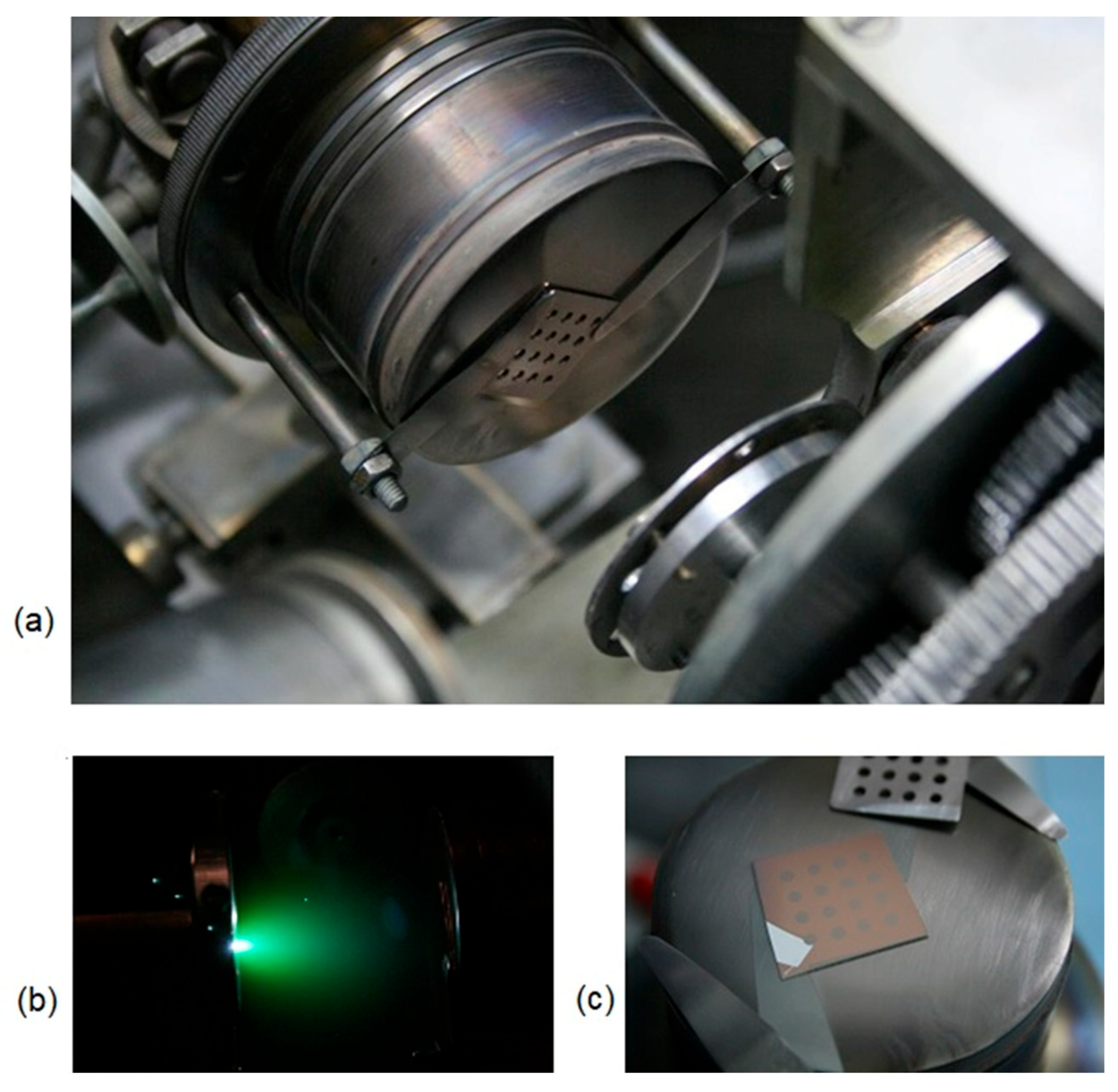
The PLD is based on the ablation of material from a solid target when its surface is irradiated with energetic, short laser pulses (10−9–10−15 s) of a focused beam at a suitable wavelength in the infrared (IR), visible, or ultraviolet (UV) range. The high-power density at the focal spot generates a plasma plume, expanding perpendicularly to the target surface. The substrate is positioned a few centimetres away, facing the plume, as illustrated in Figure 1. Detailed descriptions of the setup and procedure are available elsewhere [13].
For this study, Co and Cu targets (5 mm thick, 20 mm diameter, 99.9% purity) were mounted on the multi-target carousel of the PLD system. Substrates included Si(100) wafers, Crown borosilicate (BK7) glass substrates, and SITAL ceramics [22]. SITAL, commercially known as Sitall CO-115M or Astrositall, are glass–crystalline/glass–ceramic materials obtained by volume crystallization of glasses and consisting of one or more crystalline phases uniformly distributed in the glassy phase, characterized by an ultra-low coefficient of thermal expansion which ensures excellent dimensional stability under thermal cycling. This property makes it particularly attractive as a substrate for thin film growth, since it minimizes thermally induced stress, improves adhesion, and helps preserve interface integrity in multilayered structures such as Co/Cu spin-valves. No intentional post-deposition annealing or field-cooling procedure was applied, ensuring that the magnetic response reflects the intrinsic properties of the as-grown multilayers. The choice of substrate plays a critical role in determining the growth dynamics and resulting properties of Co/Cu multilayers. In this work, the three types of substrates were selected to provide distinct surface conditions in terms of structural order, surface energy, and roughness. Si(100) represents a well-defined crystalline substrate, offering relatively controlled nucleation conditions, whereas SITAL and BK7 are non-single-crystalline materials with inherently different surface morphologies and defect distributions. In such systems, where lattice matching is not strictly applicable, film growth is primarily governed by surface-driven processes, including nucleation density, adatom mobility, and interface formation mechanisms. These factors are expected to influence the initial growth of Co layers, the development of interfacial roughness, and ultimately the magnetotransport properties. By systematically comparing these substrates, the present study aims to elucidate the role of substrate-induced structural variations in controlling the GMR response of PLD-grown multilayers. This approach also enables evaluation of whether increased structural disorder, often considered detrimental, may in certain cases enhance GMR sensitivity through modified scattering mechanisms. Prior to deposition, all substrates were cleaned in an ultrasonic bath for 15 min in acetone, rinsed with isopropanol and deionized water, then dried under a dry air flow. These substrate types were chosen to assess adhesion, film–substrate interface quality, and the effect of morphology on thin film growth. Co/Cu multilayers also served directly as electrodes for magnetotransport measurements. A thin metallic mask was placed directly on the substrate surface to define the deposition geometry of the Co/Cu multilayers, as presented in Figure 1c and Figure 2a. While this approach allows for precise control of the active area, e.g., circular pads for transport measurements, it also introduces edge-shadowing effects due to the partial obstruction of the expanding laser-induced plume. As a result, the deposited film thickness and morphology exhibit gradients near the mask edges, with smoother and more uniform growth in the central regions. These effects are inherent to masked PLD and must be considered when analyzing surface roughness or transport properties, since they may locally influence interface quality and device reproducibility. To minimize such artefacts, it is advisable to slightly elevate the mask above the substrate (micrometre-scale spacing) or to adjust plume incidence and mask geometry, thereby reducing direct shadowing and promoting more homogeneous deposition. Depositions were carried out by using a pulsed Nd:YAG laser (“Surelite II”, Continuum) operating at 266 nm, with a 7 ns pulse duration and 10 Hz repetition rate. The laser spot was ~1 mm2, with a fluence of 4 J·cm−2, applied over 20,000 pulses. This relatively high laser fluence, and the nanosecond pulse duration, place the deposition in a regime where both energetic particle bombardment and transient thermal effects contribute to interface formation and intermixing. A target–substrate distance of 4 cm was maintained. For each run, films were simultaneously grown on both SITAL and silicon substrates, with stacks of 10, 20, or 40 Co/Cu bilayers. The nominal thicknesses correspond to individual layer thicknesses of ~16 nm for Co and ~23 nm for Cu, resulting in total multilayer thicknesses depending on the number of bilayer repetitions. Substrates were kept at room temperature under a background pressure of 7·10−5 mbar during deposition.

2.2. Thin Film Analysis

Surface morphology and nanoscale roughness of the Co/Cu multilayers were investigated by atomic force microscopy (AFM, Park XE-100, Park Systems, Gwacheon, Republic of Korea), operated in non-contact mode with a silicon carbide (SiC) cantilever tip of ~10 nm radius. This configuration provided high-resolution topographic maps across scan areas up to 20 × 20 µm2, enabling quantitative analysis of RMS roughness, grain size, and particulate distribution. Complementary imaging at larger scales was carried out by scanning electron microscopy (SEM, Inspect F FEG-SEM, Hillsboro, OR, USA), operated at acceleration voltages between 200 V and 30 kV, with a lateral resolution of ~2 nm, allowing detailed visualization of pad geometry, droplet density, and surface continuity from the millimetre down to the sub-micrometre scale. Depth profiling and interfacial composition analyses were performed using a combined secondary ion mass spectrometry/secondary neutral mass spectrometry (SIMS/SNMS) system (Hiden Analytical, Warrington, UK). This setup, equipped with a quadrupole mass spectrometer and capable of operating at high primary ion current densities (up to 1 mA), provided depth resolutions of ~1–5 nm, a mass detection range of 0–300 amu, and detection limits approaching 1 ppm, allowing precise assessment of interdiffusion and multilayer integrity [13]. This setup enabled the periodic alternation of Co and Cu layers to be resolved, while the slope of the elemental transitions was used to assess interface sharpness and possible interdiffusion. It should be noted, however, that the apparent interface width derived from SIMS/SNMS depth profiles may be influenced by intrinsic measurement artefacts. In particular, ion beam-induced mixing during sputtering, finite depth resolution, and surface roughness convolution can lead to an artificial broadening of the elemental transitions. As a result, the measured interface thickness represents an upper bound of the actual physical intermixing. Nevertheless, since all samples were analyzed under identical experimental conditions, the comparative trends observed between multilayers with different numbers of repetitions and on different substrates remain reliable. Therefore, the relative sharpening of Co/Cu interfaces in higher-period multilayers can be confidently attributed to improved growth stability and reduced interdiffusion, rather than to artefacts of the measurement technique. In addition, trace impurities at the parts-per-million (ppm) level could be detected, allowing identification of contaminants potentially segregated at interfaces. By comparing multilayers with different repetition numbers and grown on different substrates, SIMS/SNMS provided direct evidence of how deposition conditions and substrate type influenced interface integrity and, consequently, the magnetotransport properties of the Co/Cu sequences. Magnetic measurements were carried out by using a vibrating sample magnetometer (VSM, Lake Shore 7600 Series, Westerville, OH, USA), while magnetotransport aspects have been conducted by a Hall-effect experimental system. The system allows precise determination of hysteresis loops and magnetic parameters, with a typical measurement uncertainty within ±1–2%, depending on sample geometry and calibration conditions. This combination of complementary techniques offered a multi-scale, correlative view of the surface morphology, microstructural quality, chemical depth profiles, and magnetotransport performance of the PLD-grown Co/Cu multilayers.

3. Results and Discussion

The structural, morphological, and magnetotransport properties of Co/Cu multilayers grown by pulsed laser deposition (PLD) were systematically investigated as a function of substrate type and the number of bilayer repetitions. Particular attention was given to the influence of microstructure, interface roughness, and particulate formation on the giant magnetoresistance (GMR) response [23,24,25]. AFM analyses provided quantitative insight into nanoscale roughness and grain size, while SEM imaging revealed the overall pad geometry and the lateral distribution of particulates across the film surface. Complementary magnetotransport measurements demonstrated the direct correlation between interface density and field sensitivity, with 40-period multilayers exhibiting the highest ΔR/R values. The combined analysis highlights both the strengths of PLD for fabricating multilayered spin-valve structures and the characteristic challenges associated with particulate formation, ultimately providing a coherent picture of structure–property relationships in Co/Cu multilayers.

3.1. Surface Quality: Morphology and Roughness

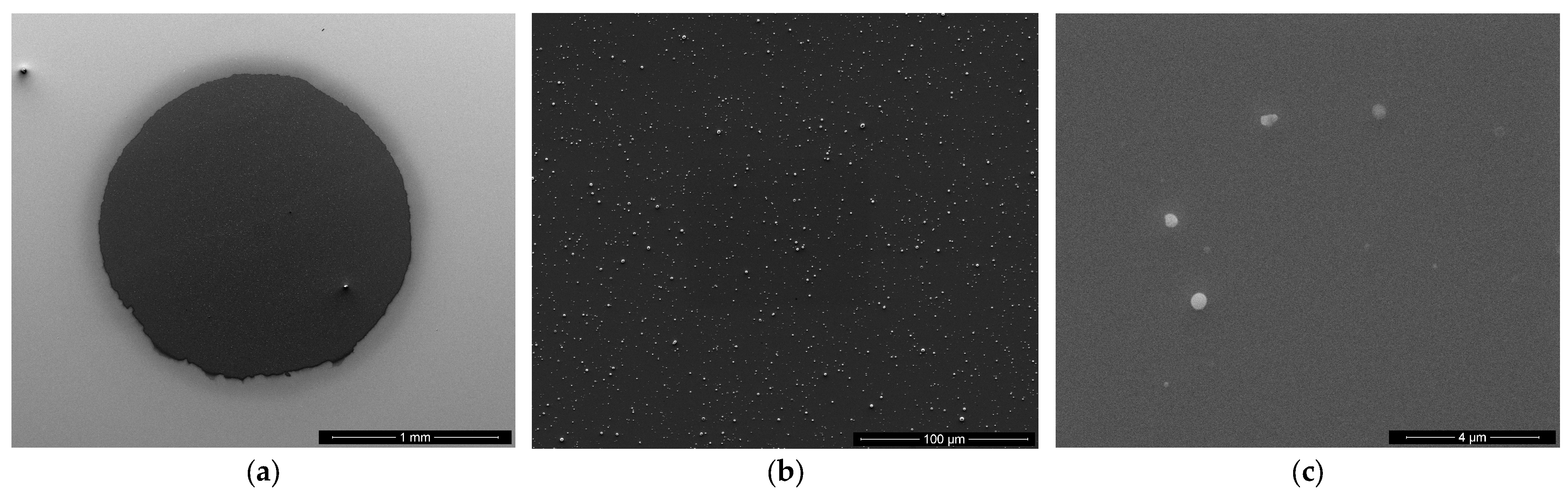
The SEM and AFM analysis of the thin film surface revealed a relatively smooth surface, with a homogeneous distribution of micron- and submicron-sized droplets, characteristic of PLD growth, as presented in Figure 2 and Figure 3, respectively. The SEM images in Figure 2 show the surface morphology of Co/Cu multilayers with 40 repetitions, grown by PLD and patterned for magnetoresistive measurements. At low magnification (Figure 2a), the circular deposition area with a diameter of approximately 2 mm is clearly visible, corresponding to the masked pad geometry used for GMR characterization.
The film covers the substrate uniformly within the defined region, with sharp edges dictated by the mask, ensuring reproducible electrode contacts for magnetotransport experiments. At intermediate magnification (Figure 2b), the surface reveals a high density of bright droplets distributed across the pad. These features are characteristic of PLD-grown metallic films and are typically associated with molten material and/or splashing events during laser ablation. These droplets appear uniformly distributed, suggesting consistent deposition conditions across the full pad area. At high magnifications (Figure 2c), the droplets are resolved more clearly, showing spherical or irregular morphologies with diameters typically between 200 nm and 1 µm. The underlying surface appears smooth and continuous, indicating that the multilayers maintain good integrity despite the presence of particulates. Such droplets, while introducing localized roughness and potential scattering centres, do not compromise the overall continuity of the Co/Cu multilayers. Taken together, these SEM analyses confirm that the PLD process yields well-defined patterned Co/Cu multilayer pads suitable for GMR measurements. The circular geometry ensures compatibility with electrical probing, while the microstructural features highlight the balance between smooth background film growth and the presence of particulates, a common characteristic of laser-based deposition techniques.
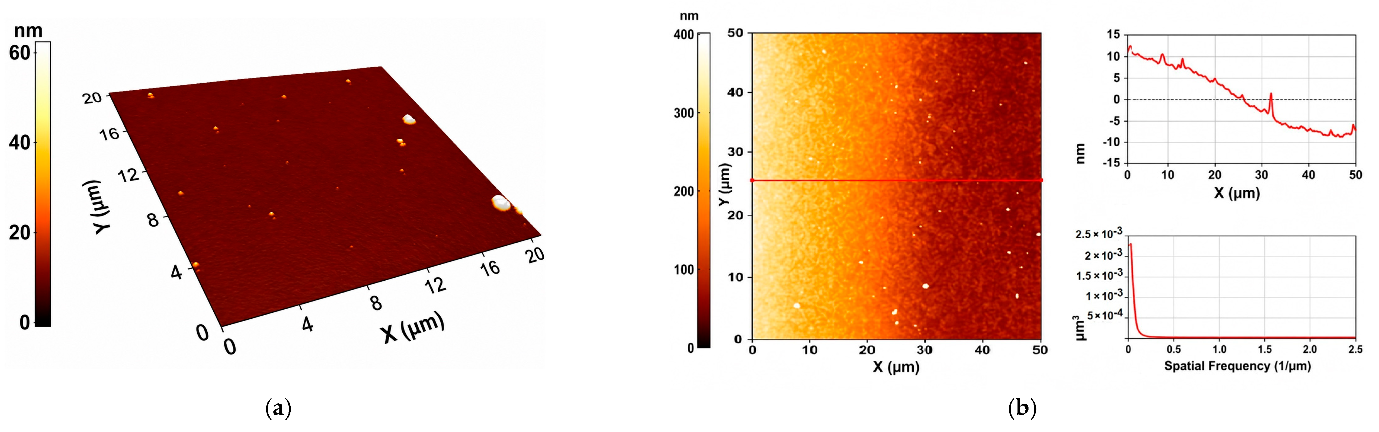
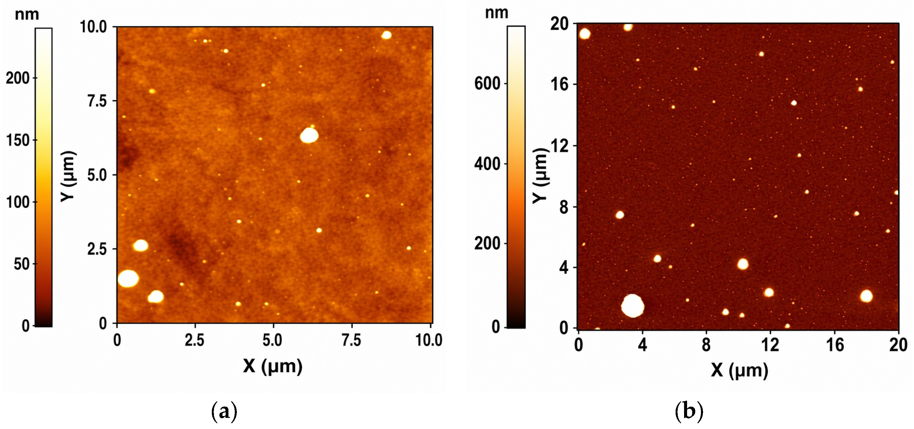
The AFM 3D topography in Figure 3a represents a Cu thin film grown on BK7 glass (20 × 20 µm2 scan area) for testing purposes. This image reveals a surface that is largely flat and continuous, with a low background roughness. The film exhibits several bright protrusions scattered across the surface, corresponding to particulates or nano-islands with heights up to ~40–50 nm. These features are sparse and non-uniform in distribution, suggesting that they originate from localized nucleation events or ejected particulates during PLD. The underlying film remains smooth, indicating good substrate coverage and uniform growth. Excluding the tallest particulates, the background surface roughness (expressed as RMS, root mean square) is expected to be very low, typically in the 1–3 nm range for PLD-grown metallic films on glass. This analysis confirms that the PLD-grown Cu thin film on BK7 glass is structurally uniform with low roughness, while occasional particulates contribute to localized surface defects. The low RMS roughness supports good optical quality, essential for magneto-optical applications and/or even for plasmonics [26,27], whereas the particulates may act as scattering centres or influence subsequent multilayer growth. Optimizing deposition parameters (e.g., laser fluence, repetition rate, or substrate–target geometry) would help reduce such particulates and further improve surface smoothness. The AFM micrograph in Figure 3b corresponds to a Cu thin film deposited on BK7 glass, where a metallic mask was employed during growth to define the circular deposition area, as presented in the SEM image from Figure 2a. The image clearly shows edge-shadowing effects, visible as a gradient in surface contrast from left to right. This shadowing is produced by the partial obstruction of the ablation plume at the mask edges, which leads to variations in local film thickness and surface morphology across the scanned region. Despite this gradient, the central areas of the film remain continuous, with a relatively uniform grain distribution at the nanoscale. The height profile confirms a smooth decrease in thickness toward the masked region, while the power spectral density analysis indicates a predominance of low-frequency roughness components, consistent with the shadow-induced modulation rather than intrinsic surface granularity. Such effects are characteristic of masked PLD processes and must be considered when fabricating patterned multilayers or sensor devices, as they can locally alter both structural uniformity and magnetotransport properties [28,29,30]. The AFM analysis of the Co/Cu multilayer with 40 repetitions deposited on SITAL ceramic (10 × 10 µm2 scan area) presented in Figure 4a reveals a continuous film with a granular texture and occasional droplets scattered across the surface. The background surface exhibits a relatively low roughness, with an estimated RMS value of ~4–6 nm, characteristic of PLD-grown metallic multilayers. When the taller droplets are included, the RMS roughness increases to ~12–15 nm, confirming their significant contribution to surface inhomogeneity. The lateral grain size is in the range of 80–150 nm, consistent with metallic multilayer growth. The overall morphology indicates that the multilayer remains structurally uniform, with good adhesion to the ceramic substrate, while the presence of droplets is attributed to splashing and ejection during PLD. Such features are characteristic of PLD growth on ceramic substrates. Importantly, the increased interface density achieved in the 40-period structure strongly favours GMR enhancement, making SITAL-supported multilayers highly promising for sensor applications. In Figure 4b, the AFM image shows the surface morphology of a Co/Cu multilayer with 40 repetitions deposited on a Si(100) substrate, scanned over a 20 × 20 µm2 area. The film exhibits a smooth and uniform background, with nanoscale roughness characteristic of PLD-grown metallic multilayers.
The RMS roughness is estimated to be ~3–5 nm across the flat regions, indicating good structural quality and coherent growth on the crystalline silicon substrate. Bright droplets are visible across the surface, with heights ranging from ~100 nm up to ~600 nm, as shown by the colour scale. These features are sparse, with a density of ~0.03–0.05 µm−2, and likely originate from splashing or droplet ejection during laser ablation. Compared to similar multilayers grown on SITAL ceramics, the Si (100) substrate yields a smoother overall surface with fewer high-aspect defects, which is advantageous for reproducibility and integration into microelectronic devices. Nonetheless, the occasional droplets may still act as localized scattering centres, potentially affecting transport uniformity in sensor applications. Thus, a direct comparison between the AFM surface morphologies of 40-period Co/Cu multilayers grown on SITAL ceramics and Si (100) substrates highlights the influence of the substrate on microstructural quality. The higher roughness and defect density are attributed to the polycrystalline and relatively rough nature of the ceramic substrate. In contrast, the Si (100)-based multilayer displays a smoother background, with an RMS roughness of ~3–5 nm. These differences underline the dual effect of substrate choice: SITAL promotes enhanced diffuse spin-dependent scattering at interfaces, which contributes to an increase in GMR amplitude, while Si ensures smoother growth and better reproducibility, more suitable for integration into microelectronic devices.
To further rationalize the influence of surface morphology on magnetotransport properties, the role of interface roughness in spin-dependent scattering must be considered. In multilayer systems, electron transport across successive Co/Cu interfaces is governed by a combination of specular and diffuse scattering processes. For relatively smooth interfaces, as observed for Si(100)-supported multilayers, electron reflection remains predominantly specular, preserving momentum and resulting in lower spin-dependent scattering asymmetry. In contrast, increased roughness, as measured on SITAL-supported films (RMS ~4–6 nm, locally higher when particulates are included), promotes diffuse scattering, where electron trajectories are randomized at the interfaces. This enhances spin-dependent scattering probabilities and contributes to an increase in the GMR response. From a semi-classical perspective, when the characteristic roughness becomes comparable to the electron mean free path, scattering at interfaces becomes more effective, leading to a stronger modulation of resistance between antiparallel and parallel magnetic configurations. These considerations provide a physical framework linking the AFM-derived roughness to the observed enhancement of GMR sensitivity on rougher substrates, while also highlighting the trade-off between structural coherence and scattering efficiency. Such morphological features are expected to directly influence spin-dependent scattering by locally modifying interface roughness and electronic mean free paths.

3.2. Magnetoresistive Response

The magnetoresistive behaviour of the Co/Cu multilayers was investigated by measuring the field-dependent resistance of circular pads patterned during deposition. Electrical contacts were established using a standard four-probe geometry with fine silver wires bonded to the film surface, ensuring low contact resistance and reproducible measurements. A constant current in the milliampere range was applied, and the longitudinal voltage drop was recorded as a function of the applied magnetic field. The relative magnetoresistance was defined as ΔR/R = (R(H) − R(0))/R(0), where R(H) is the resistance under magnetic field and R(0) is the zero-field resistance. Measurements were performed in the field range 0.01–0.625 T, enabling analysis of both the amplitude of the GMR effect and the linear response region. Particular attention was given to the influence of the bilayer repetition number, substrate type, and interfacial quality on ΔR/R amplitude and field sensitivity, which are critical parameters for evaluating multilayers in view of spin-valve and magnetic sensor applications [31,32,33]. This behaviour reflects the cumulative enhancement of spin-dependent scattering at successive Co/Cu interfaces, consistent with the two-current transport model.
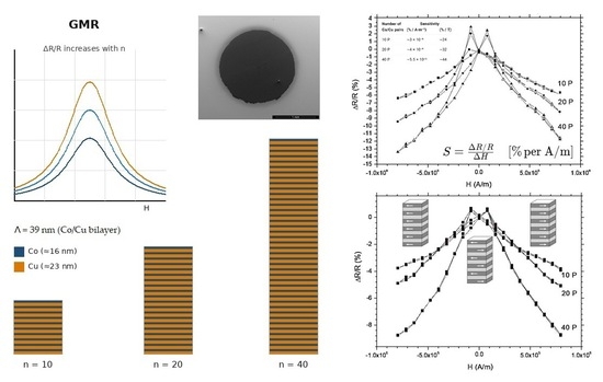
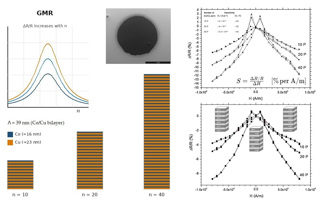
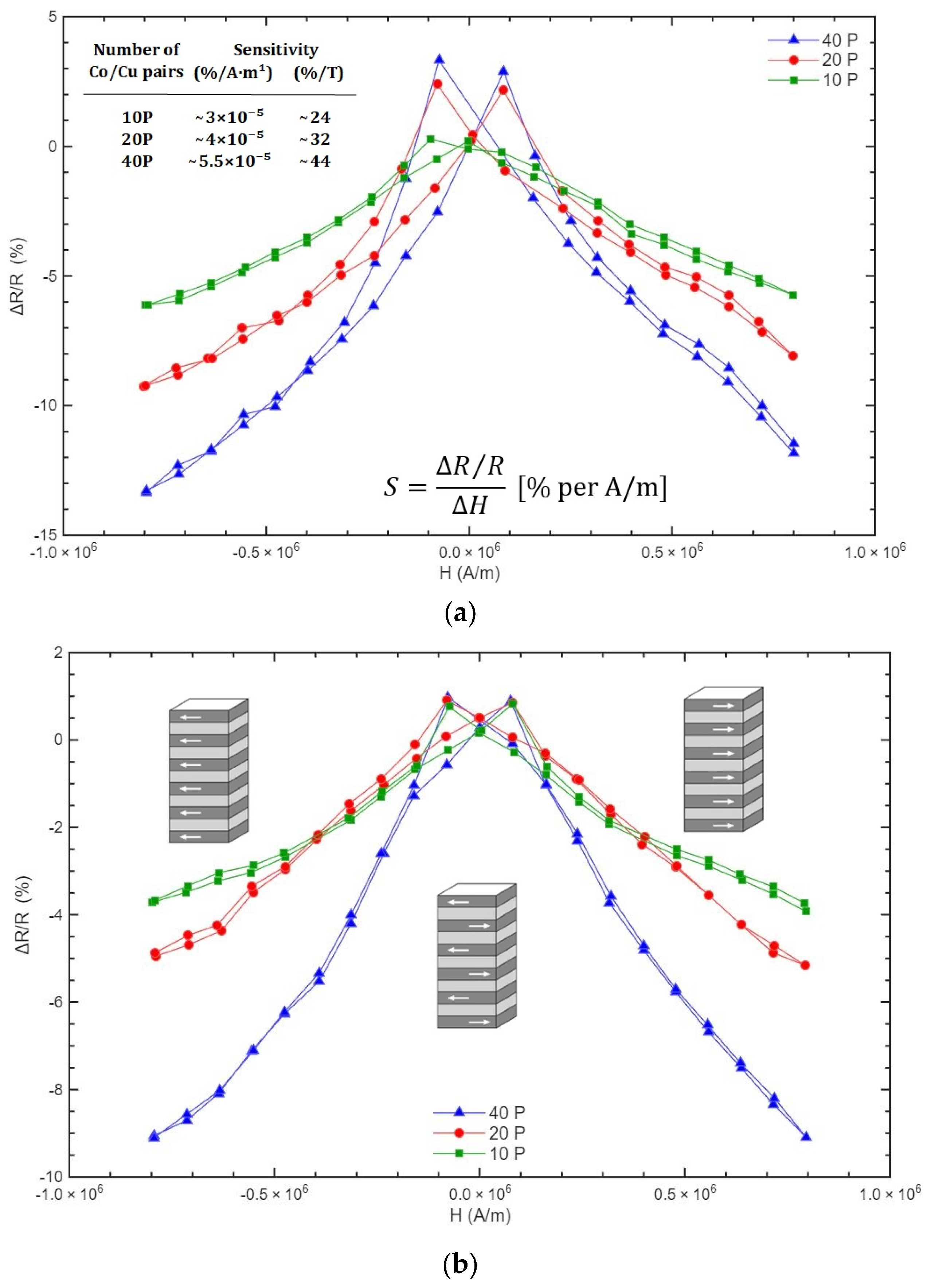
The magnetoresistive response of Co/Cu multilayers on SITAL ceramic with 10, 20, and 40 bilayer repetitions is shown in Figure 5a. All three structures exhibit a negative magnetoresistance, with a characteristic symmetric dependence on the applied magnetic field, typical of spin-valve-type systems. The maximum relative resistance change (ΔR/R) increases with the number of repetitions, reaching values close to −14% for the 40-period sample, compared to ~−9% and ~−6% for the 20- and 10-period samples, respectively. This trend reflects the cumulative contribution of additional Co/Cu interfaces, which enhance spin-dependent scattering and thereby amplify the GMR effect. The sharper magnetoresistance features and increased sensitivity indicate enhanced spin-dependent scattering efficiency, likely associated with improved interface coherence. These results highlight the direct correlation between multilayer periodicity and magnetotransport efficiency, confirming that increasing the number of Co/Cu bilayers is an effective strategy to optimize GMR performance in PLD-grown heterostructures. The magnetoresistive response of Co/Cu multilayers deposited on Si(100) substrates with 10, 20, and 40 repetitions is presented in Figure 5b. The insets show, schematically, the alignment of the magnetization directions in the Co layers. The amplitude of the resistance change increases systematically with the number of bilayers: the 10-period structure shows a maximum variation of ~−4%, while the 20- and 40-period stacks reach ~−6% and ~−9%, respectively. This trend highlights the cumulative effect of additional Co/Cu interfaces, which enhance spin scattering efficiency and strengthen the GMR effect. Compared with multilayers grown on SITAL ceramics, the Si (100) substrate provides smoother interfaces but also influences the absolute MR amplitude, likely due to differences in lattice mismatch, film adhesion, and strain. The results confirm that substrate choice plays a key role in determining the structural and magnetotransport properties of PLD-grown Co/Cu multilayers, with interface density and growth conditions acting as decisive factors for optimizing GMR performance.
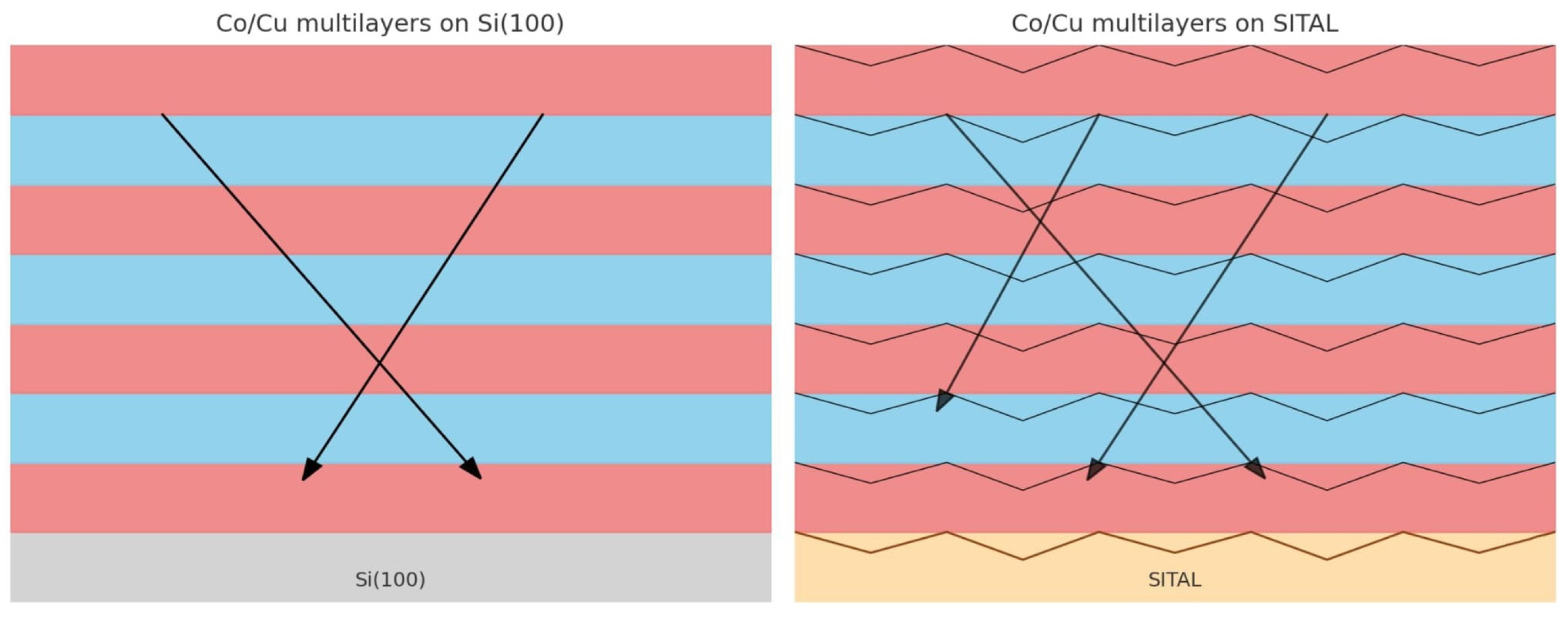
A direct comparison between Co/Cu multilayers grown on Si (100) and on SITAL ceramics reveals clear substrate-dependent effects on the magnetoresistive response. As illustrated in Figure 6, the substrate plays a decisive role in shaping the interface morphology and, consequently, the magnetotransport response of PLD-grown Co/Cu multilayers. While Si(100) substrates yield smoother interfaces and more coherent spin transport, SITAL ceramics enhance diffuse scattering at rougher interfaces, thereby amplifying the GMR signal despite reduced crystallinity. On Si(100), the maximum ΔR/R reaches ~−9% for 40-period stacks, while on SITAL the response extends to ~−14% under similar conditions. This difference can be attributed to substrate-induced microstructural variations: Si(100) promotes smoother surfaces and more coherent interfaces, but the reduced lattice mismatch and lower roughness limit the degree of spin-dependent scattering. In contrast, the polycrystalline nature and higher surface roughness of SITAL ceramics enhance diffuse scattering at Co/Cu interfaces, amplifying the overall GMR effect despite slightly less controlled crystallinity. Si-grown multilayers provide superior structural quality and reproducibility, whereas SITAL-grown films maximize sensitivity, making them particularly promising for sensor applications. In summary, Co/Cu multilayers on SITAL ceramics yield higher GMR amplitudes due to enhanced diffuse scattering at rougher interfaces, whereas Si(100) substrates provide smoother growth and reproducibility at the expense of sensitivity. In practice, Si substrates are better suited for integration with microelectronic platforms, while SITAL ceramics offer a robust alternative for standalone magnetic field detectors requiring high sensitivity. These findings highlight the versatility of PLD for tailoring Co/Cu multilayers to specific functional requirements, depending on the targeted device architecture, when compared to the literature [34,35,36,37]. To further rationalize the observed magnetoresistive behaviour, the GMR response of the Co/Cu multilayers can be interpreted in terms of spin-dependent scattering and interface-controlled transport. Within the two-current conduction framework, the total resistance arises from parallel spin channels whose scattering rates are strongly modulated by the magnetic configuration of adjacent Co layers. In the antiparallel state, electron spins experience enhanced scattering due to alternating magnetic potentials across successive layers, leading to higher resistance. Upon application of a magnetic field, the progressive alignment of the Co layer magnetizations reduces this spin-dependent scattering, resulting in a decrease in resistance and the characteristic negative magnetoresistance observed experimentally. The increase in GMR amplitude with the number of bilayers is primarily attributed to the cumulative contribution of Co/Cu interfaces, which act as dominant scattering centres for spin-polarized electrons. A higher interface density increases the probability of spin-dependent scattering events, thereby amplifying the overall magnetoresistive response. This behaviour is consistent with the two-current model, where an increased imbalance between spin-up and spin-down conduction channels enhances the resistance contrast between antiparallel and parallel magnetic states. In addition, the substrate-dependent differences observed between SITAL and Si(100) samples can be directly linked to variations in interface morphology and scattering mechanisms. The relatively higher roughness and structural disorder of SITAL-supported multilayers promote diffuse spin-dependent scattering at Co/Cu interfaces, which enhances the GMR amplitude. In contrast, the smoother interfaces obtained on Si(100) substrates favour more coherent (specular) electron transport, reducing scattering asymmetry and thus limiting the magnitude of the magnetoresistive response, while improving transport stability and reproducibility. Interfacial diffusion further modulates the GMR effect by altering the sharpness of the Co/Cu interfaces. As evidenced by SIMS/SNMS depth profiling, increased interdiffusion leads to a partial mixing of Co and Cu at the interfaces, which reduces spin selectivity and weakens the GMR response. Conversely, sharper interfaces in higher-period multilayers preserve spin-dependent scattering asymmetry, contributing to both enhanced magnetoresistance and improved Hall mobility. These combined effects demonstrate that the magnetotransport properties of PLD-grown Co/Cu multilayers are governed by a delicate balance between interface density, structural coherence, and diffusion-driven intermixing. This interpretation is fully consistent with the structural observations and reinforces the dominant role of interface morphology in governing both magnetic and magnetotransport properties in PLD-grown multilayers. These magnetotransport trends are closely reflected in the magnetic response of the multilayers, as discussed in the following section.

3.3. Magnetic Properties

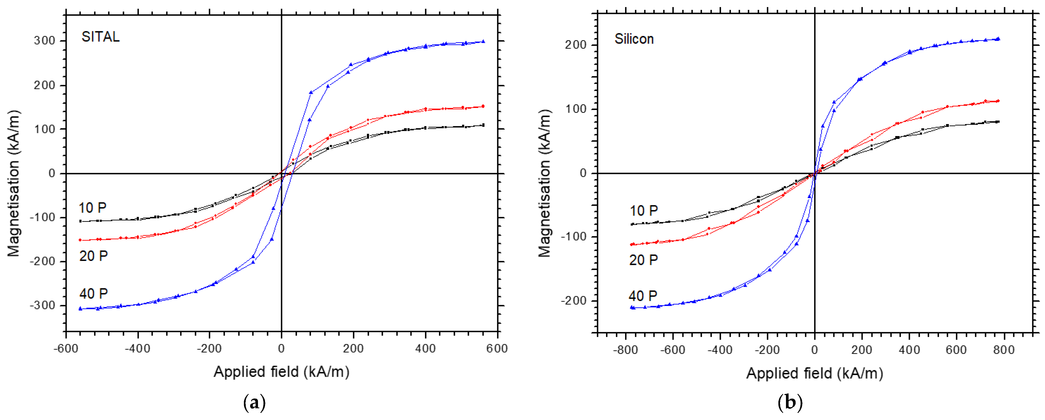
The hysteresis cycles of Co/Cu multilayers with 10, 20, and 40 repetitions deposited on SITAL ceramic substrates, presented in Figure 7a, confirm their soft magnetic character and highlight the effect of multilayer periodicity on magnetic performance. A slight asymmetry can be observed in the hysteresis loop of the 40-period multilayer. However, this feature does not indicate the presence of an exchange bias effect, as no antiferromagnetic pinning layer (e.g., FeMn, IrMn, or NiO) is incorporated in the present Co/Cu multilayer structures. In conventional exchange-biassed systems, a loop shift arises from interfacial exchange coupling between ferromagnetic and antiferromagnetic layers, typically established after field cooling through the Néel temperature, conditions that are not applicable here. The observed asymmetry is therefore more likely related to extrinsic effects associated with the microstructure of PLD-grown films, such as interfacial roughness/droplets, slight thickness variations, and structural inhomogeneities. In addition, residual stress and growth-induced anisotropy may introduce a weak unidirectional contribution, which may locally modify domain nucleation and magnetization reversal pathways. No systematic loop shift or training effect characteristic of exchange bias was observed, further supporting this interpretation. All samples display ferromagnetic-like behaviour with low coercive fields (~12–20 kA·m−1) and modest remanence, resulting in squareness ratios of only ~0.13–0.16, indicative of weak pinning and easy magnetization rotation.
The observed variation in coercivity with the number of bilayer repetitions can be directly related to structural uniformity and interface quality within the multilayer stack. In thinner structures (10-period multilayers), local thickness fluctuations, interfacial roughness, and partial intermixing can act as pinning centres for domain-walls, leading to slightly higher coercive fields. As the number of bilayers increases, the growth process becomes progressively more stable, resulting in improved layer continuity and reduced thickness dispersion across the stack. This enhanced structural uniformity facilitates smoother domain wall propagation and reduces pinning effects, thereby lowering the coercivity in thicker multilayers. Such behaviour is consistent with the evolution of interface sharpness observed in SIMS/SNMS profiles and the improved morphological homogeneity revealed by AFM analysis.
The saturation magnetization increases systematically with the number of bilayers, from ~100 kA·m−1 for 10 repetitions to ~150–160 kA·m−1 for 20 and up to ~290–300 kA·m−1 for 40, reflecting the larger ferromagnetic volume and stronger cumulative interfacial coupling in thicker stacks. At the same time, the 40-period sample exhibits the steepest slope near zero field (highest initial susceptibility, ~0.35–0.40) together with the lowest coercivity, which together favour efficient domain-wall motion and spin alignment under small applied fields. These features, combined with the enhanced magnetoresistive response already observed in transport measurements, demonstrate that PLD-grown Co/Cu multilayers on SITAL substrates act as soft magnetic systems with tunable properties, making them highly promising for spin-valve and magnetic sensor applications. Figure 7b shows the hysteresis cycles of Co/Cu multilayers with 10, 20, and 40 repetitions deposited on silicon substrates, providing insight into how the substrate influences their magnetic properties. All samples display soft ferromagnetic behaviour with low coercive fields, consistent with efficient magnetization reversal and weak domain pinning. The saturation magnetization increases systematically with the number of bilayers, from ~80 kA/m for 10 repetitions to ~120 kA/m for 20 and reaching ~200 kA/m for 40 periods. Compared to the SITAL-based multilayers, the Si/SiO2-grown films exhibit overall lower saturation values, reflecting the smoother surface and reduced interfacial scattering associated with crystalline substrates. At the same time, the sharper slope near zero field in the 40-period sample indicates a higher initial susceptibility, beneficial for spin alignment in low-field conditions. These results confirm that silicon substrates promote more coherent growth and reproducibility, while still enabling tunable soft magnetic properties with increasing multilayer thickness, making them highly relevant for integration with microelectronic platforms [38,39,40].
A slight asymmetry is observed for the 40-period Co/Cu multilayer deposited on SITAL. However, the loop does not show a pronounced lateral displacement, step-like reversal, or minor-loop character. From Figure 7a, the possible horizontal shift is estimated to remain below ~5–10 kA·m−1, i.e., less than ~2% of the full applied-field range, and is therefore too small to be assigned to a robust exchange-bias effect. This is consistent with the absence of an intentional antiferromagnetic pinning layer and with the fact that no field-cooling procedure was applied. Similarly, no significant vertical shift is observed with respect to the saturation magnetization, indicating that any uncompensated or pinned magnetic contribution, if present, remains minor. The observed asymmetry is therefore more consistently attributed to non-uniform domain-wall propagation within a heterogeneous pinning landscape, rather than to a true exchange-bias mechanism [41,42,43,44,45]. Pronounced asymmetric magnetization reversal, often associated with clear hysteresis-loop shifts and enhanced coercivity, is typically observed in exchange-biassed systems such as CoO/Co bilayers, Co/CoO granular films, and Co/Pt multilayers, where interfacial coupling between ferromagnetic and antiferromagnetic phases plays a dominant role [46,47,48]. In contrast, in multilayered systems as is the case for the present Co/Cu multilayers, such behaviour may arise from local variations in interface roughness, thickness, residual stress, droplet density, or defect distribution, which generate spatially heterogeneous pinning landscapes for domain-wall motion. This interpretation is supported by reports showing that asymmetric reversal can originate from dipolar coupling and domain-wall pinning in multilayers, even when the asymmetry is not associated with a conventional exchange-bias mechanism. Gottwald et al. showed that asymmetric reversal in coupled multilayers can arise from magnetic domains and stray field-induced pinning, while simulations of structured ferromagnetic systems have shown that random anisotropy, hard/soft regions, and defects can generate asymmetric or pseudo-exchange-bias-like loops even in the absence of an antiferromagnetic layer [49,50]. In the present PLD-grown Co/Cu multilayers, this effect is expected to be amplified in the 40-period SITAL sample because the higher number of Co/Cu interfaces increases the probability of cumulative roughness, local interfacial disorder, and magnetostatic coupling between neighbouring magnetic layers. The SITAL substrate further promotes a rougher growth morphology compared with Si(100), which can enhance local anisotropy variations and domain-wall pinning. A contribution from trace oxidation cannot be fully excluded, especially at Co-rich interfaces or free surfaces, but the absence of a clear loop shift, strong coercivity enhancement, or training-like behaviour indicates that oxide-related exchange bias is not the dominant mechanism. Interfacial Dzyaloshinskii–Moriya interaction is also unlikely to be the main origin, since the present structure does not include a heavy-metal interface designed to generate strong spin–orbit coupling, and the literature on Co thin films indicates that DMI-related chiral asymmetry is not generally relevant for inversion-symmetric metallic systems. Overall, the weak asymmetry observed in the 40-period SITAL sample is best interpreted as a morphology- and defect-assisted reversal asymmetry, governed by domain-wall pinning, local anisotropy variations, and magnetostatic interactions accumulated across the multilayer stack, rather than by a genuine exchange-bias effect. This interpretation is fully consistent with the structural observations and reinforces the dominant role of interface morphology in governing both magnetic and magnetotransport properties in PLD-grown multilayers.
To conclude, a direct comparison of the hysteresis loops obtained for Co/Cu multilayers deposited on SITAL ceramics and silicon substrates reveals both similarities and distinct substrate-driven differences. In both cases, the films exhibit soft magnetic behaviour characterized by low coercivity and weak remanence, which are essential features for spin-valve applications where rapid and reversible magnetization switching is required. However, the SITAL-based multilayers consistently reach higher saturation magnetization values (up to ~300 kA·m−1 for 40 repetitions) compared to those grown on silicon (~200 kA·m−1), a result of enhanced diffuse scattering and interface roughness in the ceramic-supported films that amplify spin-dependent contributions. Conversely, the silicon samples display smoother hysteresis curves with lower absolute magnetization but improved reproducibility and sharper near-zero-field slopes, reflecting more coherent growth and reduced structural disorder at the interfaces. For spin-valve devices, these differences imply a trade-off: SITAL substrates favour stronger GMR signals and higher sensitivity due to enhanced scattering, whereas silicon substrates offer better structural uniformity and integration compatibility with microelectronics, supporting stable and reproducible device operation.

3.4. Charge Carrier Density and Hall Mobility Analysis

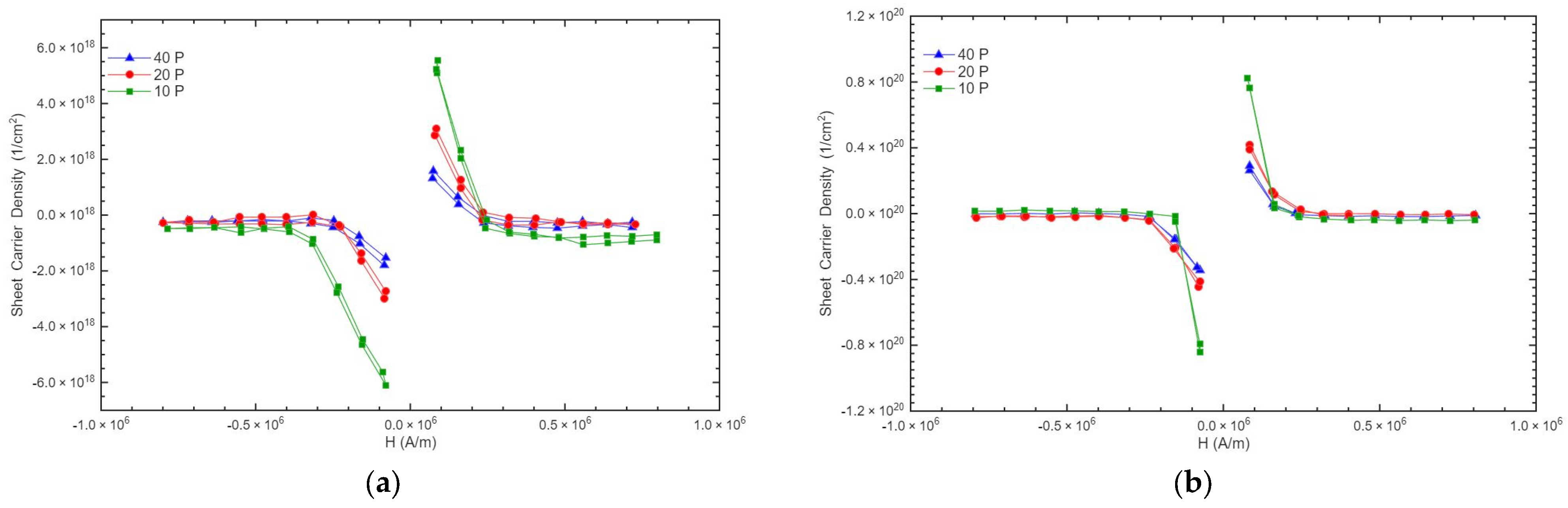
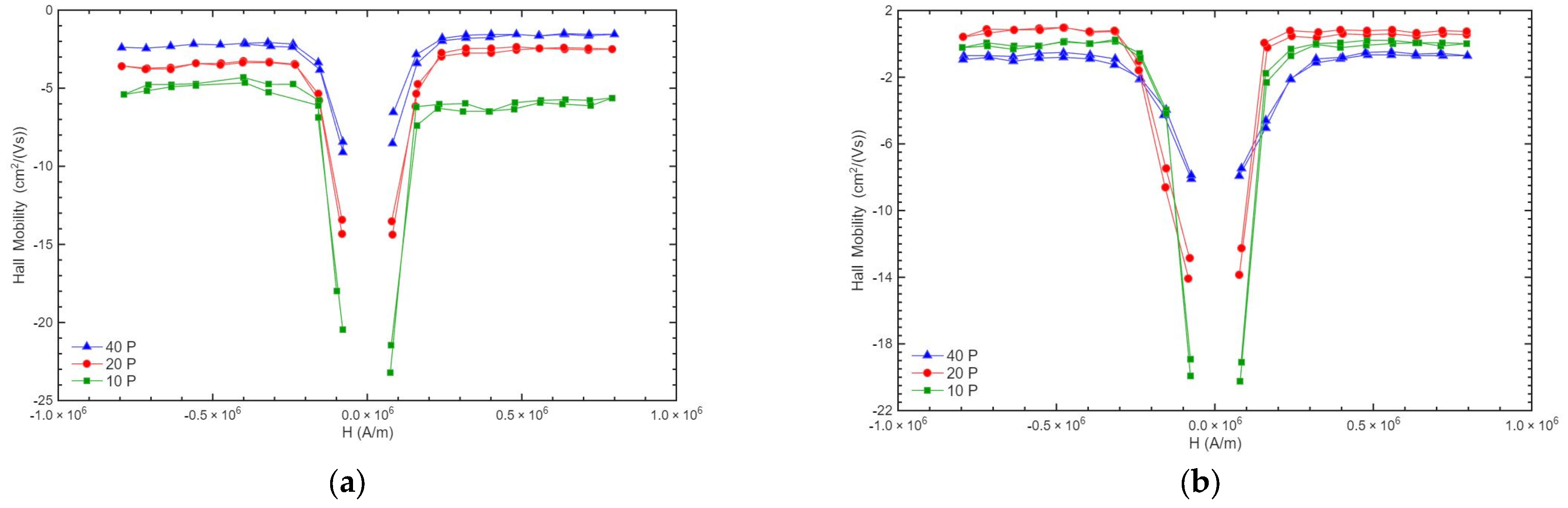
The Hall effect measurements performed on Co/Cu multilayers grown on SITAL ceramics provide complementary insights into their charge transport properties. In contrast to SITAL-based multilayers (Figure 7), the Si-supported samples (Figure 8) provide an insight into the variation in the sheet carrier density with applied magnetic field (Figure 8a) revealing a strong field dependence, particularly in the 10-period multilayer where the carrier density changes abruptly, reaching values on the order of 1018 cm−2. In contrast, the 20- and 40-period samples show more stable behaviour, with smaller fluctuations around zero field and a faster convergence to steady-state values at higher fields. This stabilization with increasing repetitions reflects improved multilayer continuity and interface quality, reducing localized charge trapping and interdiffusion effects. The corresponding Hall mobility curves (Figure 9a) show a clear dependence on bilayer number: the 10-period sample exhibits the lowest mobilities (with sharp drops near zero field, down to −20 cm2/V·s), while the 20- and 40-period samples sustain higher and more stable mobilities, reaching values of −5 to −3 cm2/V·s under applied fields.
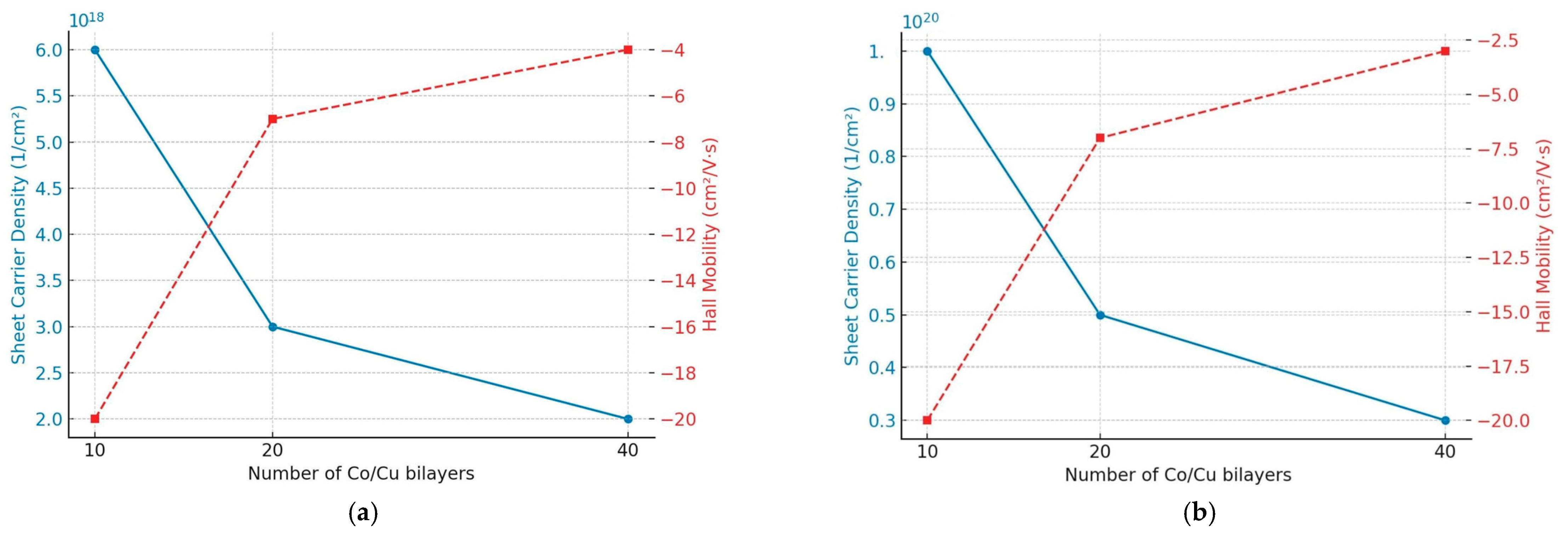
The enhanced mobility in thicker multilayers is consistent with better-defined Co/Cu interfaces, which favour coherent charge transport and reduced scattering. When compared to the literature reports on sputtered or MBE-grown Co/Cu multilayers, where typical Hall mobilities are in the range of −1 to −10 cm2/V·s and carrier densities remain around 1018–1019 cm−2, the PLD-grown SITAL-based films exhibit competitive transport properties despite the presence of PLD-induced particulates [51,52,53]. These results confirm that increasing the number of bilayers not only enhances the GMR response but also improves the electronic transport stability, consolidating the role of PLD as a viable method for fabricating spin-valve architectures with tunable charge carrier dynamics. The simultaneous decrease in carrier density and increase in mobility suggests a transition toward more coherent transport regimes as interface quality improves. A comparison of the Hall effect results for Co/Cu multilayers grown on SITAL ceramics (Figure 9a) and on silicon substrates (Figure 9b) highlights the strong influence of the substrate on charge transport. In both cases, increasing the number of bilayers leads to a reduction in sheet carrier density and a simultaneous increase in Hall mobility, reflecting improved multilayer continuity and better-defined interfaces. However, the absolute values differ significantly: SITAL-based multilayers (Figure 10b) exhibit lower carrier densities (~1018 cm−2) and moderate mobilities (–5 to −4 cm2/V·s for 40 periods), while silicon-supported (Figure 10b) films show higher carrier densities (~1019–1020 cm−2) and more pronounced improvements in mobility with increasing thickness (from −20 cm2/V·s in 10-period stacks to ~−3 cm2/V·s in 40-period samples). These differences can be attributed to the smoother and more coherent interfaces formed on crystalline silicon, which promote efficient charge transport but maintain higher carrier concentrations, versus the rougher SITAL substrates, where enhanced diffuse scattering lowers carrier density but also limits mobility gains.
From a spintronic perspective, SITAL-grown films are advantageous for maximizing GMR sensitivity due to stronger spin-dependent scattering, while silicon samples offer superior electronic transport stability and are better suited for integration with microelectronic platforms [51,52,53].

3.5. Interfacial Phenomena, Interdiffusion and Chemical Composition

In PLD, the interfacial structure of multilayers is strongly governed by the kinetic energy and temporal characteristics of the ablated species, which are directly controlled by the laser parameters (fluence, pulse duration, and repetition rate). Under the present deposition conditions (266 nm wavelength, 7 ns pulse duration, and fluence of ~4 J·cm−2), the ablation process generates a highly energetic plasma plume containing ions, atoms, and clusters with kinetic energies typically in the range of a few to several tens of eV. Upon arrival at the substrate, these species can induce localized atomic displacements and promote ballistic mixing at the growing interfaces. In parallel, the transient thermal load associated with each laser pulse leads to rapid local heating followed by ultrafast cooling, creating non-equilibrium conditions that enhance short-range diffusion across Co/Cu interfaces. As a result, the effective interface width is determined by the combined contribution of ballistic intermixing and thermally activated diffusion processes. This explains the broadened elemental transitions observed in SIMS/SNMS depth profiles for low-period multilayers, where cumulative interface roughness and incomplete layer stabilization promote interdiffusion. Conversely, in thicker multilayers (20–40 periods), the progressive stabilization of the growth front and improved layer continuity limit intermixing, leading to sharper interfaces and enhanced spin-dependent scattering asymmetry. These observations establish a direct link between PLD parameters, interfacial diffusion, and the resulting magnetotransport properties.
The interfacial analysis by SIMS/SNMS depth profiling provided direct evidence of the interfacial properties within the Co/Cu multilayers. In samples with a low number of repetitions, e.g., 10 periods, the elemental transitions between Co and Cu layers appeared broadened, indicating partial interdiffusion and reduced interface sharpness. This observation correlates with the AFM and SEM results, where higher surface roughness and particulates were more pronounced, and with the transport data, where lower Hall mobilities and weaker GMR amplitudes were measured.
A semi-quantitative estimation of the interface width can be obtained from the slope of the Co and Cu signals in the SIMS/SNMS depth profiles. Considering the instrumental depth resolution (≈1–5 nm) and the observed transition gradients, the effective interface width is estimated to be on the order of ~6–10 nm for 10-period multilayers, decreasing to ~3–6 nm for 20 periods and approaching ~2–4 nm for the 40-period stacks. Although these values include contributions from sputter-induced broadening, they clearly indicate a progressive sharpening of the interfaces with increasing numbers of bilayers. This trend suggests that the characteristic diffusion length scale is reduced as the multilayer growth becomes more stable, which is consistent with the improved morphological uniformity and enhanced magnetotransport performance observed in thicker stacks.
In contrast, the 20- and especially the 40-period multilayers exhibited sharper and more periodic Co/Cu profiles, with reduced intermixing at the interfaces. These results are consistent with smoother background morphology, higher magnetic susceptibility, and enhanced GMR response, alongside stabilized Hall carrier densities and improved mobility. Importantly, the SIMS/SNMS analysis also revealed substrate-related effects: films grown on silicon showed generally sharper interfaces compared to those on SITAL, in line with their smoother AFM surface and lower roughness, while SITAL-based samples, although exhibiting slightly more interfacial diffusion, benefited from stronger spin-dependent scattering that boosted GMR amplitudes. Altogether, these findings confirm that interface sharpness plays a decisive role in governing magnetotransport properties, linking structural integrity at the nanoscale to the macroscopic performance of spin-valve architectures.
To conclude, the estimated sensitivities clearly show that the magnetoresistive response strengthens with the number of bilayers. The 40-period multilayers exhibit the steepest slope in the ΔR/R–H curve, reaching ~44%/T, almost twice the value of the 10-period samples. This trend confirms that increasing the number of Co/Cu interfaces enhances spin-dependent scattering and thus amplifies the GMR effect. The higher interface density in the 40-period structures not only improves sensitivity but also contributes to a more linear response around zero field, which is particularly advantageous for magnetic sensor applications. SIMS/SNMS depth profiles confirmed that multilayers with higher repetition numbers exhibited sharper Co/Cu interfaces and reduced interdiffusion, consistent with the enhanced GMR amplitudes and stabilized Hall transport properties, whereas broader elemental transitions in thinner stacks correlated with lower mobility and weaker magnetoresistive response. When compared with the literature values for sputtered Co/Cu spin-valves, where field sensitivities typically range between 20 and 50%/T depending on microstructural quality and interface engineering [54,55,56], the PLD-grown multilayers reported here show competitive performance. In particular, the 40-period PLD samples approach the upper end of reported sensitivities, underscoring the potential of laser-based deposition for fabricating high-quality multilayers. This is noteworthy, since sputtering is usually considered the benchmark technique for GMR devices, while PLD offers additional flexibility in substrate choice, stoichiometric transfer, and excellent film growth control [57,58,59].
To provide a concise comparison of the structural, magnetotransport, and charge transport parameters across all investigated samples, the main results are summarized in Table 1. Beyond the individual trends observed in morphology, magnetotransport, and magnetic response, the present results highlight a broader conceptual outcome: the GMR performance of Co/Cu multilayers can be deliberately engineered through the combined control of interface density, substrate-induced morphology, and laser-driven growth conditions. In this context, possible oxidation of Co and Cu layers must also be considered when analyzing multilayer integrity. Under the present deposition conditions (base pressure ~7 × 10⁻⁵ mbar and room temperature growth), oxidation is expected to be limited. SIMS/SNMS depth profiles did not reveal significant oxygen-related signals correlated with the Co/Cu interfaces, indicating that no substantial oxide layer formation occurred within the detection limits of the technique. While trace oxygen contamination at the ppm level cannot be completely excluded, its contribution is expected to be negligible compared to the dominant effects of interfacial roughness and interdiffusion. This is further supported by the strong GMR response observed, since significant Co oxidation (e.g., CoO formation) would reduce spin polarization and suppress the magnetoresistive effect. Therefore, oxidation does not appear to play a major role, and the observed magnetotransport behaviour can be primarily attributed to structural and interfacial phenomena intrinsic to the PLD growth process.
To place these results in a broader context, it is worth noting that magnetotransport in Cu–Co-based systems is governed by a delicate interplay between microstructure, interface characteristics, and scattering length scales, rather than by geometrical thickness alone. Previous studies on Cu–Co granular thin films have shown that the electron mean free path is typically on the order of a few nanometres, comparable to the characteristic size of structural inhomogeneities, thereby emphasizing the dominant role of nanoscale interfaces in limiting transport properties [60]. In such systems, competing mechanisms, such as surface scattering, microstructural evolution, and variations in spontaneous magnetization, may partially compensate each other, leading to non-trivial or weak thickness dependencies of the magnetoresistive response. Although the present Co/Cu multilayers differ from granular systems in their layered architecture, a similar physical picture emerges, in which magnetotransport is primarily controlled by interface density, interfacial roughness, and local structural disorder. This comparison supports the interpretation that the enhanced GMR response observed in the present PLD-grown multilayers originates from the cumulative contribution of spin-dependent scattering at multiple Co/Cu interfaces, rather than from a purely geometrical thickness effect, highlighting the central role of interface engineering.
Unlike conventional sputtered systems, where interface quality is largely governed by near-equilibrium growth processes, PLD operates in a highly non-equilibrium regime that enables simultaneous tuning of interfacial roughness, interdiffusion, and spin-dependent scattering. This provides an additional degree of freedom for optimizing the balance between sensitivity and structural coherence. As a result, PLD-grown multilayers offer a versatile pathway toward application-specific design, ranging from high-sensitivity magnetic sensors (favoured by diffuse scattering on SITAL) to reproducible, device-integrated architectures (enabled by smoother Si-based growth). This behaviour can be interpreted within a diffusion-limited growth framework, where the effective interfacial broadening δ scales with the square root of the diffusion coefficient and interaction time (δ ~ √Dt), indicating that the stabilization of the growth front in higher-period multilayers effectively limits atomic intermixing.
To provide a broader physical perspective on the present results, it is important to clarify the origin of the slight asymmetry observed in the magnetization reversal, particularly for the 40-period multilayer on SITAL. Although a weak deviation from perfect symmetry is detected, the absence of a clear horizontal loop shift, coercivity enhancement, or field-history dependence indicates that this behaviour cannot be attributed to a true exchange-bias effect, which is typically associated with interfacial coupling between ferromagnetic and antiferromagnetic phases and manifests as a measurable loop displacement along the field axis [46,47,48]. Instead, the observed behaviour is more consistent with a pseudo-exchange-bias-like asymmetry, as reported in structurally inhomogeneous or purely ferromagnetic systems, where local variations in magnetic anisotropy and morphology can lead to asymmetric reversal without the presence of an antiferromagnetic pinning layer [49,50]. In this framework, magnetization reversal is governed by heterogeneous domain nucleation and domain-wall pinning within a spatially non-uniform energy landscape, arising from interface roughness, droplet density, and local thickness variations, which collectively define a complex pinning environment. This interpretation is further supported by studies showing that asymmetric hysteresis behaviour can originate from differences in nucleation processes and domain-wall propagation mechanisms between the ascending and descending branches of the loop [41,42,43,44,45]. More generally, these results highlight the central role of interface engineering in determining both magnetic and magnetotransport properties in Co/Cu multilayers. As widely established in spintronic systems, spin-dependent scattering and magnetization dynamics are strongly governed by interfacial characteristics, including roughness, interdiffusion, and structural coherence [1,2]. In this context, the progressive increase in GMR amplitude with the number of bilayers confirms that the magnetoresistive response is primarily controlled by interface density rather than by the total thickness of the multilayer stack, consistent with models in which electron mean free paths are comparable to the characteristic length scale of interfacial scattering. Therefore, PLD-grown Co/Cu multilayers can be positioned within the broader class of structurally disordered ferromagnetic systems in which both magnetotransport and magnetic reversal are dominated by interfacial effects. This provides a coherent framework linking the enhanced GMR response and the observed reversal asymmetry to a common physical origin rooted in interface-controlled spin-dependent transport and domain-wall dynamics.


4. Conclusions

This study demonstrates that the magnetotransport properties of Co/Cu multilayers can be actively engineered through PLD-driven control of the interface structure and substrate-dependent growth. By varying both the number of bilayer repetitions and the substrate type, we demonstrate that the GMR response can be effectively tuned through interface engineering at the nanoscale. Increasing the number of Co/Cu bilayers leads to a higher interface density, which enhances spin-dependent scattering and results in a significant amplification of the magnetoresistive response. The 40-period multilayers exhibit the highest GMR amplitude (up to ~−14%) and field sensitivity (~44%·T−1), together with improved magnetic susceptibility and reduced coercivity, confirming their suitability for spin-valve and sensor applications. SIMS/SNMS profiles indicate comparatively sharper interfaces and reduced interdiffusion, directly correlating with enhanced transport stability and improved Hall mobility. A key outcome of this study is the identification of a strong substrate-dependent effect. SITAL ceramic substrates promote increased interface roughness and diffuse scattering, leading to enhanced GMR sensitivity, whereas Si(100) substrates enable smoother growth, improved structural coherence, and more stable charge transport. This highlights a fundamental trade-off between maximizing magnetoresistive response and ensuring device reproducibility and integration compatibility. Compared to conventional sputtered or MBE-grown systems, the PLD approach offers distinct advantages, including precise control of multilayer architecture, efficient stoichiometric transfer, and the ability to tailor interfacial properties through localized energy input. Despite the presence of PLD-induced particulates, the magnetotransport performance remains competitive with state-of-the-art multilayers, demonstrating the robustness of this technique. Overall, this study establishes PLD as a powerful and flexible platform for the design of Co/Cu multilayers with tunable structural and functional properties. The ability to control interfacial scattering mechanisms through both deposition parameters and substrate selection opens new perspectives for optimizing spintronic devices, particularly in the development of high-sensitivity magnetic sensors and next-generation spin-valve architectures. Importantly, this work demonstrates that laser-based deposition is not merely an alternative fabrication technique, but a powerful tool for actively controlling spin-dependent transport mechanisms in multilayer systems, thereby opening new directions for the design of next-generation spintronic materials and devices. These findings establish PLD not only as a deposition technique, but as a powerful tool for engineering spin-dependent transport through controlled deviation from ideal interface conditions.

Author Contributions

Conceptualization, C.-D.C.; methodology, C.-D.C. and L.-G.P.; validation, C.-D.C., E.-A.P., N.-D.S., A.-N.M., A.-G.N., C.-R.L., C.C., M.-C.P. and L.-G.P.; formal analysis, C.-D.C., E.-A.P., C.C., M.-C.P. and L.-G.P.; investigation, C.-D.C., E.-A.P., C.C., M.-C.P. and L.-G.P.; resources, C.-D.C., E.-A.P., C.C., M.-C.P. and L.-G.P.; data curation, C.-D.C., E.-A.P., C.C. and M.-C.P.; writing—original draft preparation, L.-G.P., C.-D.C. and L.-G.P.; writing—review and editing, C.-D.C., E.-A.P., C.C., M.-C.P. and L.-G.P.; visualization, C.-D.C. and L.-G.P.; supervision, C.-D.C. and L.-G.P.; project administration, C.-D.C. and L.-G.P.; funding acquisition, C.-D.C. and L.-G.P. All authors have read and agreed to the published version of the manuscript.

Funding

This research received no external funding.

Data Availability Statement

Data available upon reasonable request to the corresponding authors.

Acknowledgments

The authors (C.-D.C.; E.-A.P.; C.C.; M.-C.P.; L.-G.P.) would like to acknowledge the late Horia Gavrila for his invaluable assistance in our training during the doctoral thesis period.

Conflicts of Interest

The authors declare no conflicts of interest. The funders had no role in the design of the study; in the collection, analyses, or interpretation of data; in the writing of the manuscript; or in the decision to publish the results.

References

  1. Baibich, M.N.; Broto, J.M.; Fert, A.; Nguyen Van Dau, F.; Petroff, F.; Etienne, P.; Creuzet, G.; Friederich, A.; Chazelas, J. Giant Magnetoresistance of (001)Fe/(001)Cr Magnetic Superlattices. Phys. Rev. Lett. 1988, 61, 2472–2475. [Google Scholar] [CrossRef]
  2. Binasch, G.; Grünberg, P.; Saurenbach, F.; Zinn, W. Enhanced Magnetoresistance in Layered Magnetic Structures with Antiferromagnetic Interlayer Exchange. Phys. Rev. B 1989, 39, 4828–4830. [Google Scholar] [CrossRef] [PubMed]
  3. Parkin, S.S.P.; More, N.; Roche, K.P. Oscillations in Exchange Coupling and Magnetoresistance in Metallic Superlattice Structures: Co/Ru, Co/Cr, and Co/Cu. Phys. Rev. Lett. 1990, 64, 2304–2307. [Google Scholar] [CrossRef]
  4. Piraux, L.; George, J.M.; Despres, J.F.; Leroy, C.; Ferain, E.; Legras, R.; Ounadjela, K.; Fert, A. Giant Magnetoresistance in Magnetic Multilayered Nanowires. Appl. Phys. Lett. 1994, 65, 2484–2486. [Google Scholar] [CrossRef]
  5. Parkin, S.S.P.; Modak, A.; Smith, D.J. Dependence of giant magnetoresistance on Cu-layer thickness in Co/Cu multilayers: A simple dilution effect. Phys. Rev. B 1993, 47, 9139(R). [Google Scholar] [CrossRef]
  6. Holloway, H.; Kubinski, D.J. Magnetoresistive Co/Cu multilayers: Hysteresis, polycrystallinity, and irreversible changes on magnetization. J. Appl. Phys. 1998, 83, 2705–2714. [Google Scholar] [CrossRef]
  7. Hübner, W.; Bennemann, K.H. Simple theory for spin-lattice relaxation in metallic rare-earth ferromagnets. Phys. Rev. B 1996, 53, 3422–3427. [Google Scholar] [CrossRef] [PubMed]
  8. Zhang, G.P.; Hübner, W. Laser-Induced Ultrafast Demagnetization in Ferromagnetic Metals. Phys. Rev. Lett. 2000, 85, 3025–3028. [Google Scholar] [CrossRef] [PubMed]
  9. Eason, R. (Ed.) Pulsed Laser Deposition of Thin Films: Applications-Led Growth of Functional Materials; John Wiley & Sons, Inc.: Hoboken, NJ, USA, 2006; ISBN 9780470052129. [Google Scholar] [CrossRef]
  10. Yang, D. (Ed.) Pulsed Laser Processing of Materials; IntechOpen: London, UK, 2024; ISBN 9780854666126. [Google Scholar] [CrossRef]
  11. Constantinescu, C.; Scarisoreanu, N.; Moldovan, A.; Dinescu, M.; Miron, M.; Petrescu, L. Thin films of NdFeB deposited by PLD technique. Proc. SPIE 2007, 6606, 660619. [Google Scholar] [CrossRef]
  12. Morintale, E.; Constantinescu, C.; Dinescu, M. Thin films development by pulsed laser-assisted deposition. Phys. AUC 2010, 20, 43–56. Available online: https://cis01.ucv.ro/pauc/vol/2010_20_part1/2010_part1_43_56.pdf (accessed on 2 May 2026).
  13. Constantinescu, C.; Ion, V.; Galca, A.C.; Dinescu, M. Morphological, optical and electrical properties of samarium oxide thin films. Thin Solid Film. 2012, 520, 6393–6397. [Google Scholar] [CrossRef]
  14. Vovk, V.; Schmitz, G.; Hütten, A. Mismatch-induced recrystallization of giant magnetoresistance multilayer systems. Appl. Phys. Lett. 2006, 88, 023120. [Google Scholar] [CrossRef]
  15. Mangin, S.; Ravelosona, D.; Katine, J.A.; Carey, M.J.; Terris, B.D.; Fullerton, E.E. Current-Induced Magnetization Reversal in Nanostructures. Nat. Mater. 2006, 5, 210–215. [Google Scholar] [CrossRef]
  16. Leitao, D.C.; van Riel, F.J.F.; Rasly, M.; Araujo, P.D.R.; Salvador, M.; Paz, E.; Koopmans, B. Enhanced performance and functionality in spintronic sensors. Npj Spintron. 2024, 2, 54. [Google Scholar] [CrossRef]
  17. Ulmeanu, M.; Filipescu, M.; Scărișoreanu, N.D.; Georgescu, G.; Rusen, L.; Zamfirescu, M. Selective removal and patterning of a Co/Cu/Co trilayer created by femtosecond laser processing. Appl. Phys. A 2011, 104, 247–255. [Google Scholar] [CrossRef]
  18. Wang, J.-Q.; Malkinski, L.M.; MacLaren, J.M.; Whittenburg, S.L.; O’Connor, C.J. Giant Magnetoresistance in Co/Cu/Co Pseudo Spin Valves. Mater. Sci. Forum 2001, 75, 373–376. [Google Scholar] [CrossRef]
  19. Jergel, M.; Halahovets, Y.; Šiffalovič, P.; Végsö, K.; Senderák, R.; Majková, E.; Luby, Š. Behavior of giant magnetoresistance in Co–Cu–Co pseudo spin-valves after magnetic annealing. Thin Solid Film. 2011, 520, 667–673. [Google Scholar] [CrossRef]
  20. Matsuki, K.; Ohshima, R.; Leiva, L.; Ando, Y.; Shinjo, T.; Tsuchiya, T.; Shiraishi, M. Spin transport in a lateral spin valve with a suspended Cu channel. Sci. Rep. 2020, 10, 10699. [Google Scholar] [CrossRef]
  21. Huai, Y.; Chaker, M.; Pépin, H.; Boily, S.; Bian, X.; Cochrane, R.W. Pulsed laser deposition of giant magnetoresistance Co-Cu films. J. Magn. Magn. Mater. 1994, 136, 204–208. [Google Scholar] [CrossRef]
  22. Solov’ev, V.I.; Sysoev, E.P.; Tryapkin, A.A.; Grushevskii, Y.L.; Lyubimov, I.S. Sitall from pressed and sintered fused basalt powders. Glass Ceram. 1987, 44, 418–420. [Google Scholar] [CrossRef]
  23. Gupta, A.; Paul, A.; Chaudhari, S.M.; Phase, D.M. Effect of interface roughness on GMR in Fe/Cr multilayers. J. Phys. Soc. Jpn. 2000, 69, 2182–2187. [Google Scholar] [CrossRef]
  24. Wang, Y.; Wang, H.; Zhang, Y.; Cui, S.; Hu, F.; Li, B. Integrated Microfluidic Giant Magnetoresistance (GMR) Biosensor Platform for Magnetoresistive Immunoassay of Myoglobin. Biosensors 2026, 16, 8. [Google Scholar] [CrossRef]
  25. Kac, M.; Dobrowolska, A.; Polit, A.; Żukrowski, J.; Marszalek, M. The influence of the atomic scale interface roughness on the GMR effect in Fe/Cr multilayers. J. Alloys Compd. 2020, 824, 153877. [Google Scholar] [CrossRef]
  26. Comesaña-Hermo, M.; Haltz, E.; Gabbani, A.; Pineider, F.; Salgueiriño, V. Toward enhancing chiro-optical and magneto-optical properties of magnetic nanocrystals by surface plasmons. Adv. Opt. Mater. 2025, 13, e202500682. [Google Scholar] [CrossRef]
  27. Ma, N.; Zhang, G.; Liang, H.; Gu, S.; Wang, C.; Zhang, Y.; Gao, X. Classification and Contour Recognition of Welding Defects in Magneto-Optical Images. Metals 2026, 16, 267. [Google Scholar] [CrossRef]
  28. Zhang, Y.; He, Y.; Liang, L.; Li, Z.; Yan, X.; Yao, H.; Wang, Z.; Hu, X.; Sun, Z.; Zhou, S. Amplitude and frequency dual-mode based patterned gallium nitride thin film assisted terahertz metasurface sensors for temperature measurement. Phys. Scr. 2025, 100, 095539. [Google Scholar] [CrossRef]
  29. Son, W.; Choi, L. Bias Normalization for Sensors in Smart Devices. Sensors 2025, 25, 7291. [Google Scholar] [CrossRef]
  30. Urbaniak, M.; Kiphart, D.; Matczak, M.; Stobiecki, F.; Chaves-O’Flynn, G.D.; Kuświk, P. Ferrimagnetic Tb/Co multilayers patterned by ion bombardment as substrates for magnetophoresis. Sci. Rep. 2024, 14, 23771. [Google Scholar] [CrossRef]
  31. Xu, T.; Lan, T.; Yu, J.; Fu, Y.; Li, B.; Yang, T.; Bai, R. A Novel Open-Loop Current Sensor Based on Multiple Spin Valve Sensors and Magnetic Shunt Effect with Position Deviation Calibration. Micromachines 2025, 16, 953. [Google Scholar] [CrossRef]
  32. Leitao, D.C.; Gameiro, L.; Silva, A.V.; Cardoso, S.; Freitas, P.P. Field Detection in Spin Valve Sensors Using CoFeB/Ru Synthetic-Antiferromagnetic Multilayers as Magnetic Flux Concentrators. IEEE Trans. Magn. 2012, 48, 3847–3850. [Google Scholar] [CrossRef]
  33. Jitariu, A.; Ghemes, C.; Lupu, N.; Chiriac, H. Magnetic particles detection by using spin valve sensors and magnetic traps. AIP Adv. 2017, 7, 056616. [Google Scholar] [CrossRef]
  34. Elsafi, B. Influence of reduced Cu thickness on magnetoresistance in Co/Cu multilayers: A spin-dependent scattering analysis. Appl. Phys. A 2026, 132, 287. [Google Scholar] [CrossRef]
  35. Schroeder, V.; Bass, J.; Holody, P.; Lee, S.-F.; Loloee, R.; Pratt, W.P., Jr.; Yang, Q. Perpendicular Magnetoresistance in Cu/Co and Cu/(NiFe) Multilayers. MRS Online Proc. Libr. 1993, 313, 47–52. [Google Scholar] [CrossRef]
  36. Marszałek, M.; Polit, A.; Tokman, V.; Zabila, Y.; Protsenko, I. The effect of surfactants on the growth of Co/Cu multilayers. Surf. Sci. 2007, 601, 4454–4458. [Google Scholar] [CrossRef]
  37. Tóth, B.G.; Péter, L.; Dégi, J.; Révész, Á.; Oszetzky, D.; Molnár, G.; Bakonyi, I. Influence of Cu deposition potential on the giant magnetoresistance and surface roughness of electrodeposited Ni-Co/Cu multilayers. Electrochim. Acta 2013, 91, 122–129. [Google Scholar] [CrossRef]
  38. Murcia Correa, L.S.; Usuriaga-Najera, O.C.; Berni, L.A.; Raniero, L. Cathodic Cage Plasma Deposition of Ag/Porous Silicon as a Scalable Route to SERS Substrates. Braz. J. Phys. 2026, 56, 61. [Google Scholar] [CrossRef]
  39. Aberl, J.; Vukušić, L.; Fournel, F.; Hartmann, J.M.; Brehm, M. Epitaxial Growth of Planar Hutwires on Silicon-on-Insulator Substrates. Phys. Status Solidi A Appl. Mater. Sci. 2022, 219, 2200145. [Google Scholar] [CrossRef]
  40. Meng, S.; Deng, Q.; Zhang, L.; Feng, Y.; Fan, L.; Liu, Y.; Liu, D.; Wang, C. A SERS Substrate for Ultrafast Photosynthetic Au Nanoparticle Growth on WO3 Nanowires. Colloids Interfaces 2025, 9, 70. [Google Scholar] [CrossRef]
  41. Paes, V.Z.C.; Varalda, J.; Schio, P.; Matsushima, J.T.; Pereira, E.C.; de Oliveira, A.J.A.; Mosca, D.H. Monte Carlo simulations of magnetization state of ellipsoidal CoCu particles in disordered self-assembled arrays. J. Mater. Res. 2016, 31, 2058–2064. [Google Scholar] [CrossRef]
  42. Ehrmann, A.; Blachowicz, T. Magnetization reversal asymmetry in a structured ferromagnetic nanoparticle with varying shape anisotropy. J. Magn. Magn. Mater. 2022, 546, 168929. [Google Scholar] [CrossRef]
  43. Quach, D.-T.; Chu, T.-D.; Nguyen, T.-S.; Doan, T.-T.-P.; Nguyen, X.-T.; Lee, K.-M.; Jeong, J.-R.; Kim, N.; Shin, H.-J.; Kim, D.-H. Microscopic origin of asymmetric magnetization reversal of Co/Pt multilayers with perpendicular magnetic anisotropy. Curr. Appl. Phys. 2020, 20, 1026–1030. [Google Scholar] [CrossRef]
  44. Rohart, S.; Thiaville, A. Skyrmion confinement in ultrathin film nanostructures in the presence of Dzyaloshinskii–Moriya interaction. Phys. Rev. B 2013, 88, 184422. [Google Scholar] [CrossRef]
  45. Hellman, F.; Hoffmann, A.; Tserkovnyak, Y.; Beach, G.S.D.; Fullerton, E.E.; Leighton, C.; MacDonald, A.H.; Ralph, D.C.; Arena, D.A.; Dürr, H.A.; et al. Interface-induced phenomena in magnetism. Rev. Mod. Phys. 2017, 89, 025006. [Google Scholar] [CrossRef] [PubMed]
  46. Radu, F.; Etzkorn, M.; Schmitte, T.; Siebrecht, R.; Schreyer, A.; Westerholt, K.; Zabel, H. Asymmetric magnetization reversal on exchange biased CoO/Co bilayers. J. Magn. Magn. Mater. 2002, 240, 251–253. [Google Scholar] [CrossRef]
  47. Wu, R.; Wei, J.Z.; Peng, X.L.; Fu, J.B.; Liu, S.Q.; Zhang, Y.; Xia, Y.H.; Wang, C.S.; Yang, Y.C.; Yang, J.B. The asymmetric magnetization reversal in exchange biased granular Co/CoO films. Appl. Phys. Lett. 2014, 104, 182403. [Google Scholar] [CrossRef]
  48. van Dijken, S.; Czapkiewicz, M.; Zoladz, M.; Stobiecki, T. Asymmetric magnetization reversal in exchange-biased Co/Pt multilayers. Phys. Status Solidi B 2006, 243, 2992–2997. [Google Scholar] [CrossRef]
  49. Gottwald, M.; Hehn, M.; Lacour, D.; Hauet, T.; Montaigne, F.; Mangin, S.; Fischer, P.; Im, M.-Y.; Berger, A. Asymmetric magnetization reversal in dipolarly coupled spin valve structures with perpendicular magnetic anisotropy. Phys. Rev. B 2012, 85, 064403. [Google Scholar] [CrossRef]
  50. Detzmeier, J.; Königer, K.; Blachowicz, T.; Ehrmann, A. Asymmetric hysteresis loops in structured ferromagnetic nanoparticles with hard/soft areas. Nanomaterials 2021, 11, 800. [Google Scholar] [CrossRef]
  51. Kalaycı, T. Investigation of Cap and Buffer Layer Effect in Co/Ni Thin Films by Ferromagnetic Resonance Technique. Karadeniz Fen Bilim. Derg. 2023, 13, 724–733. [Google Scholar] [CrossRef]
  52. Schindler, F.; Geilker, J.; Kwapil, W.; Warta, W.; Schubert, M.C. Hall mobility in multicrystalline silicon. J. Appl. Phys. 2011, 110, 043722. [Google Scholar] [CrossRef]
  53. Kulkarni, P.D.; Iwasaki, H.; Nakatani, T. The Effect of Geometrical Overlap between Giant Magnetoresistance Sensor and Magnetic Flux Concentrators: A Novel Comb-Shaped Sensor for Improved Sensitivity. Sensors 2022, 22, 9385. [Google Scholar] [CrossRef]
  54. Dieny, B.J. Giant magnetoresistance in spin-valve multilayers. J. Magn. Magn. Mater. 1994, 136, 335–359. [Google Scholar] [CrossRef]
  55. Fullerton, E.E.; Childress, J.R. Spintronics, magnetoresistive heads, and the emergence of the digital world. Proc. IEEE 2016, 104, 1787–1795. [Google Scholar] [CrossRef]
  56. Gallagher, W.J.; Parkin, S.S.P. Development of the magnetic tunnel junction MRAM at IBM: From first junctions to a 16-Mb MRAM demonstrator chip. IBM J. Res. Dev. 2006, 50, 5–23. [Google Scholar] [CrossRef]
  57. Djamal, M.; Ramli, R. Thin Film of Giant Magnetoresistance (GMR) Material Prepared by Sputtering Method. Adv. Mater. Res. 2013, 770, 1–9. [Google Scholar] [CrossRef]
  58. Ludwig, K.; Hauch, J.; Mattheis, R.; Barholz, K.-U.; Rieger, G. Adapting GMR sensors for integrated devices. Sens. Actuators A Phys. 2003, 106, 15–18. [Google Scholar] [CrossRef]
  59. Ma, B.; Ma, K.; Qin, X.; Xi, Y.; Zhang, J.; Yang, X.; Yang, P.; Liu, W. Effect of Hafnium-Based Thin Film Thickness on Microstructure and Electrical of Yttrium-Doped Hafnium Oxide Ferroelectric Devices Prepared by Magnetron Sputtering. Micromachines 2025, 16, 1066. [Google Scholar] [CrossRef] [PubMed]
  60. Wang, J.-Q.; Dao, N.; Kim, N.H.; Whittenburg, S.L. Thickness dependence of magneto-transport in Cu–Co granular thin films. J. Appl. Phys. 2004, 95, 6762–6764. [Google Scholar] [CrossRef]
Figure 1. PLD of Co/Cu multilayers. (a) Photograph of the PLD chamber prior to deposition, showing the substrate holder with the sample and mask installed (upper left), and the multi-target carousel with Co and Cu targets (lower right). (b) Image of the plasma plume generated during Cu ablation, exhibiting the characteristic green emission associated with copper species. (c) Photograph of the substrate holder after deposition, showing a SITAL sample with the mask removed. The circular multilayer structures are visible, together with the shadow of the initial Cu layer and the region covered by the clamp used to secure the sample and mask.
Magnetochemistry 12 00055 g001
Figure 2. SEM images of Co/Cu multilayers (40 bilayers) deposited by PLD on a SITAL substrate: (a) low-magnification view showing the circular pad geometry (~2 mm diameter) as defined by the mask; (b) intermediate magnification revealing uniform film coverage and the spatial distribution of particulates across the surface; (c) high-magnification image highlighting droplets with sizes in the range of ≈200 nm to 1 µm. Despite the presence of these particulates, the multilayer film remains continuous and structurally intact.
Magnetochemistry 12 00055 g002
Figure 3. AFM characterization of Cu thin films deposited on BK7 substrates by PLD: (a) three-dimensional surface topography (20 × 20 µm2) showing a smooth background with low roughness and dispersed particulates; (b) surface morphology highlighting edge-shadowing effects induced by the deposition mask, leading to thickness and contrast gradients near the film edge.
Magnetochemistry 12 00055 g003
Figure 4. AFM surface topography of Co/Cu multilayers (40 bilayers) deposited by PLD on (a) a SITAL substrate, showing higher local roughness (RMS ~4–6 nm, increased when particulates are included), and on (b) a Si(100) substrate, exhibiting a smoother morphology (RMS ~3–5 nm). The substrate-dependent roughness is expected to directly influence interfacial scattering and, consequently, the magnetotransport properties.
Magnetochemistry 12 00055 g004
Figure 5. Magnetoresistance response (ΔR/R) as a function of the applied magnetic field for Co/Cu multilayers with 10, 20, and 40 bilayer repetitions deposited on (a) SITAL ceramic and (b) Si(100) substrates. All samples exhibit a symmetric negative magnetoresistance, characteristic of spin-dependent transport in multilayer systems. The amplitude of the GMR effect increases systematically with the number of bilayers, reflecting the enhanced contribution of Co/Cu interfaces to spin-dependent scattering. The highest ΔR/R values are obtained for the 40-period multilayers on both SITAL and Si(100), highlighting the combined influence of interface density and substrate-dependent morphology on the magnetotransport performance.
Magnetochemistry 12 00055 g005
Figure 6. Schematic comparison of Co/Cu multilayers grown on different substrates. (Left): On Si(100), smooth interfaces promote coherent spin transport with reduced scattering, resulting in lower ΔR/R values but improved structural quality. (Right): On SITAL ceramics, the rougher substrate induces irregular interfaces and enhanced diffuse scattering, which amplifies the GMR effect despite lower crystallinity. This illustrates the dual influence of substrate type on interface morphology and magnetotransport properties.
Magnetochemistry 12 00055 g006
Figure 7. Magnetic hysteresis loops of Co/Cu multilayers with 10, 20, and 40 bilayer repetitions deposited on (a) SITAL ceramic and (b) Si(100) substrates. All samples exhibit soft ferromagnetic behaviour with low coercivity. The saturation magnetization increases with the number of bilayers and shows a clear dependence on the substrate, reflecting differences in interface structure and microstructural quality. A slight asymmetry is observed for the 40-period multilayer on SITAL (a), with a very small horizontal shift (<5–10 kA·m−1, i.e., <~2% of the applied field range) and no significant vertical offset, indicating the absence of a robust exchange-bias effect. This weak asymmetry is attributed to morphology- and defect-induced domain-wall pinning rather than to interfacial ferromagnetic/antiferromagnetic coupling.
Magnetochemistry 12 00055 g007
Figure 8. Magnetic hysteresis loops of Co/Cu multilayers deposited on Si(100): (a) full-field cycles showing saturation magnetization increasing from ~80 kA·m−1 (10 periods) to ~200 kA·m−1 (40 periods); (b) low-field region highlighting coercive fields of ~12–20 kA·m−1 and increased initial susceptibility for higher-period multilayers.
Magnetochemistry 12 00055 g008
Figure 9. Hall effect analysis of Co/Cu multilayers deposited on SITAL substrates: (a) sheet carrier density as a function of applied magnetic field; (b) corresponding Hall mobility curves, showing improved transport stability and increased mobility with increasing number of bilayer repetitions.
Magnetochemistry 12 00055 g009
Figure 10. Correlation between the number of Co/Cu bilayers, sheet carrier density, and Hall mobility for multilayers deposited on SITAL ceramics, in (a). Increasing the number of repetitions reduces the carrier density (from ~6 × 1018 cm−2 at 10 periods to ~2 × 1018 cm−2 at 40 periods) while enhancing the Hall mobility (from −20 cm2/V·s to −4 cm2/V·s), indicating improved interface continuity and more coherent charge transport in thicker multilayer stacks. In (b) is the same correlation but for CoCu films grown on silicon substrates. Yet again, with increasing repetitions, the carrier density decreases significantly (from ~1 × 1020 cm−2 for 10 periods to ~3 × 1019 cm−2 for 40 periods), while the Hall mobility increases in magnitude (from −20 cm2/V·s up to −3 cm2/V·s).
Magnetochemistry 12 00055 g010
Table 1. Summary of structural and magnetotransport properties of the Co/Cu multilayers.
Substrate TypeBilayers
(Number of Repetitions)
RMS
Roughness (nm)
ΔR/R (%)Sensitivity (%·T−1)Carrier Density (cm−2)Hall
Mobility (cm2/V·s)
SITAL10~4–6 (bg)
~12–15
(incl. droplets)
~−6~20–25~6 × 10¹⁸~−20
SITAL20~4–6 (bg)
~12–15
(incl. droplets)
~−9~30–35~3–4 × 10¹⁸~−5
SITAL40~4–6 (bg)
~12–15
(incl. droplets)
~−14~44~2 × 10¹⁸~−4
Si(100)10~3–5~−4~15–20~1 × 10²⁰~−20
Si(100)20~3–5~−6~20–25~5–7 × 10¹⁹~−6
Si(100)40~3–5~−9~30–35~3 × 10¹⁹~−3
Disclaimer/Publisher’s Note: The statements, opinions and data contained in all publications are solely those of the individual author(s) and contributor(s) and not of MDPI and/or the editor(s). MDPI and/or the editor(s) disclaim responsibility for any injury to people or property resulting from any ideas, methods, instructions or products referred to in the content.